Fund Project:Project supported by the National Natural Science Foundation of China (Grant No. 91850117)
Received Date:19 June 2020
Accepted Date:18 August 2020
Available Online:07 December 2020
Published Online:20 December 2020
Abstract:As a basic optical element, optical lens is widely used for realizing the focusing, imaging and optical communication systems. Light of different wavelengths will propagate at different speeds. A beam of polychromatic light will produce chromatic dispersion after passing through a single optical device, which prevents the ordinary lenses from focusing the light of different wavelengths into a point. This means that the light of different wavelengths cannot be focused ideally. Traditional focusing systems can solve this problem by superimposing multiple lenses, but this is at the expense of increasing the complexity, weight, and cost of the system, and is not suitable for highly integrated nano-optical systems. At present, a better solution is to use the plane metalens, that is, using the metasurface to control the amplitude, phase and polarization at each point in space. However, the plane metalens is difficult to directly integrate on the chip. An intelligent algorithm developed by combining finite element method with genetic algorithm is used to optimize the design of multi-channel on-chip wavelength router devices and polarization router devices. In this paper, combining with years’ research results of the theory of multiple scattering coherent superposition of disordered media, the use of intelligent algorithm to design an on-chip integrated nano-lens that can achieve efficient focusing from the visible to the near infrared band. In the lens structure SiO2 serves as a substrate, and the arrangement structure of SiC rectangular column is designed. The substrate size is only 2 μm × 2 μm. The lens achieves low-dispersion focusing in the band from 470 nm to 1734 nm, with a focusing efficiency of over 55% at the highest level and 30% at the lowest level, and an average focusing efficiency of 42.1%. A 200-nm waveguide is added behind the focusing region. After refocusing through the waveguide, the laser beam with a size of 2 μm can be focused by the coupling of the lens and the waveguide into a beam below 200 nm in size. The focusing efficiency goes up to 80%. At the same time, the intelligent algorithm can be applied to different types of structures. The focusing lens structures composed of triangle, diamond, or circular nano columns are designed, which can achieve an approximate focusing effect and efficient coupling propagation efficiency. This work provides important ideas for developing broadband and efficient focusing nano-lens, as well as a new way to achieve the high-density integrated nanophotonic devices. Keywords:nano-lens/ broadband efficient focusing/ on-chip integration/ intelligent algorithm
使用智能算法, 在不改变基础材料的基础上, 设计了以三角形、菱形、圆形为纳米柱结构的宽带高效聚焦结构. 其中, 三角形是腰为$ 20\sqrt{2} $ nm的等腰直角三角形, 直角指向出射方向; 菱形为边长为40 nm的正菱形, 菱形的角指向出射方向; 圆形的半径为20 nm. 优化所得结构与以800 nm为例的电场幅值分布如图7(a)—(f)所示. 聚焦效率如图8(a)—(c)所示, 由于每个形状具有不同的特点, 所以在有限的迭代次数所得到最佳的聚焦波长是不同的, 三角形结构可实现在319—1515 nm波段30%以上的聚焦效率, 平均聚焦效率为39.09%; 菱形结构可实现在702 nm至1653 nm波段30%以上的聚焦效率, 平均聚焦效率为37.14%; 圆形结构可实现在475—1750 nm波段30%以上的聚焦效率, 平均聚焦范围为40.82%. 如果增加迭代次数可得到更相近的结果. 图 7 纳米柱结构与800 nm场幅值分布 (a) 三角形结构; (b) 菱形结构; (c) 圆形结构; (d) 三角形结构场幅值分布; (e) 菱形结构场幅值分布; (f) 圆形结构场幅值分布 Figure7. Nanoparticle structure and distribution of the electric field intensity at 800 nm: (a) Triangular structure; (b) rhombic structure; (c) circular structure; (d) the electric field intensity distribution of triangular structure; (e) the electric field intensity distribution of rhombic structure; (f) the electric field intensity distribution of circular structure.
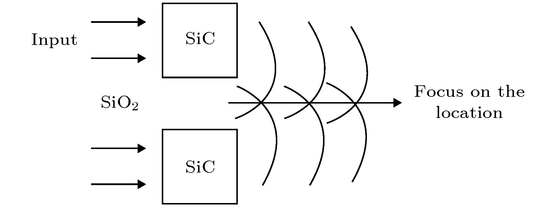 图 1 光经过碳化硅矩形后的衍射与干涉


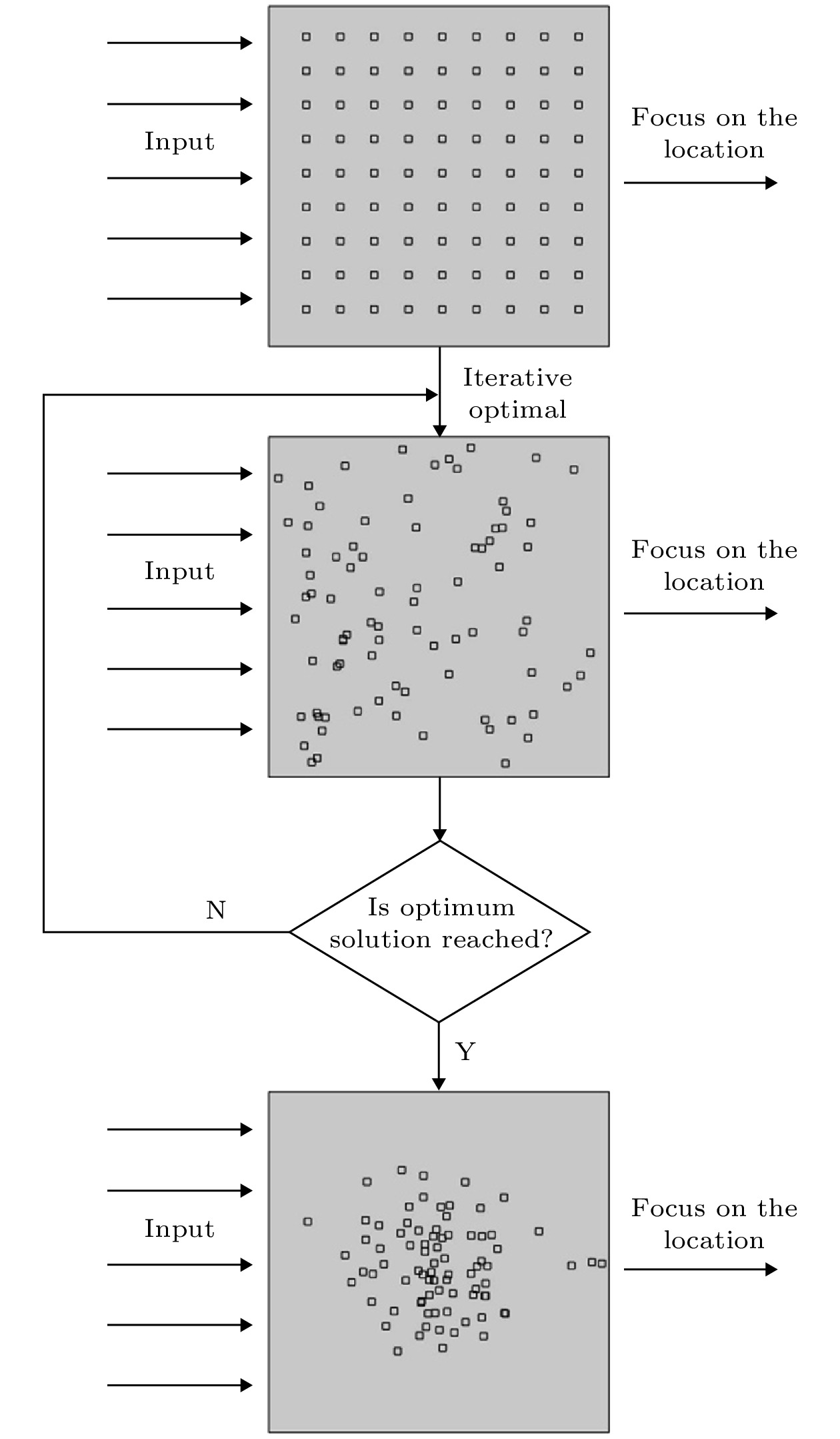 图 2 纳米透镜的结构优化示意图
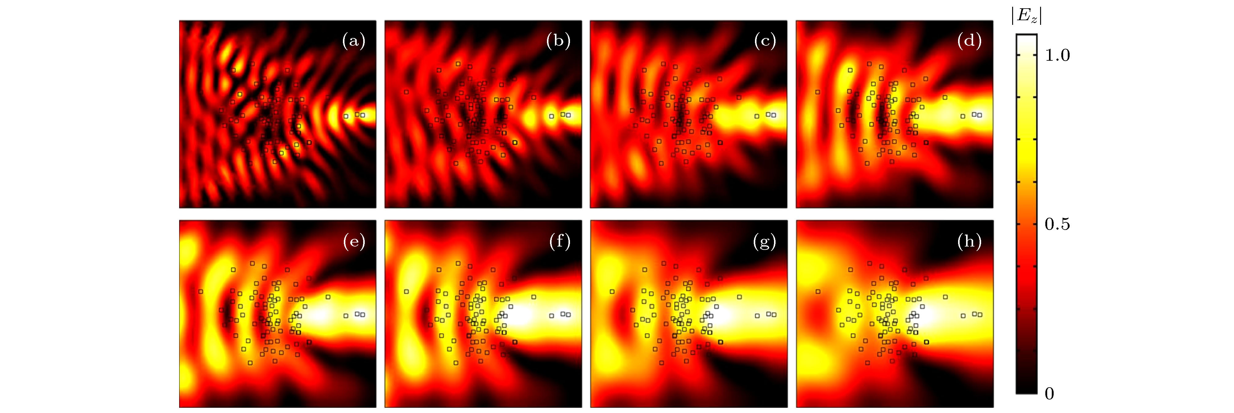 图 3 不同波长下电场幅值分布图 (a) 500 nm; (b) 650 nm; (c) 800 nm; (d) 950 nm; (e) 1100 nm; (f) 1250 nm; (g) 1400 nm; (h) 1550 nm
 图 4 对不同波长光的聚焦效率
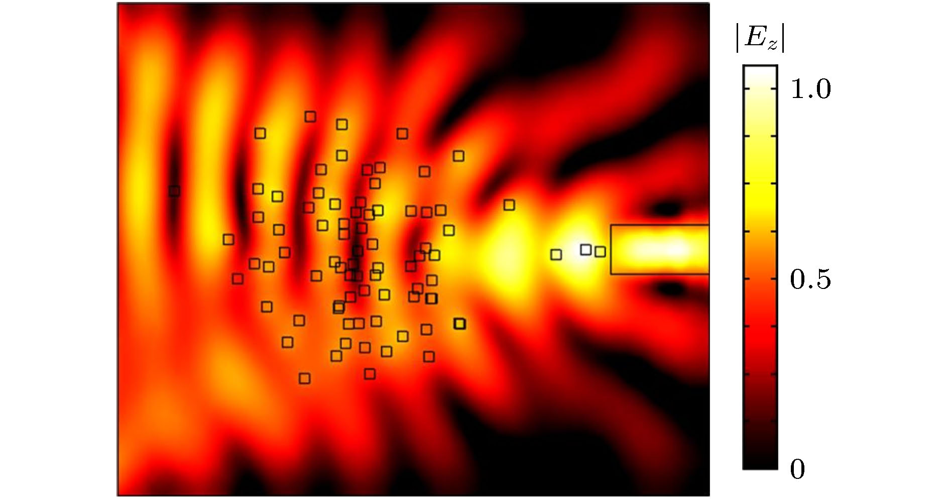 图 5 聚焦光的波导耦合输出
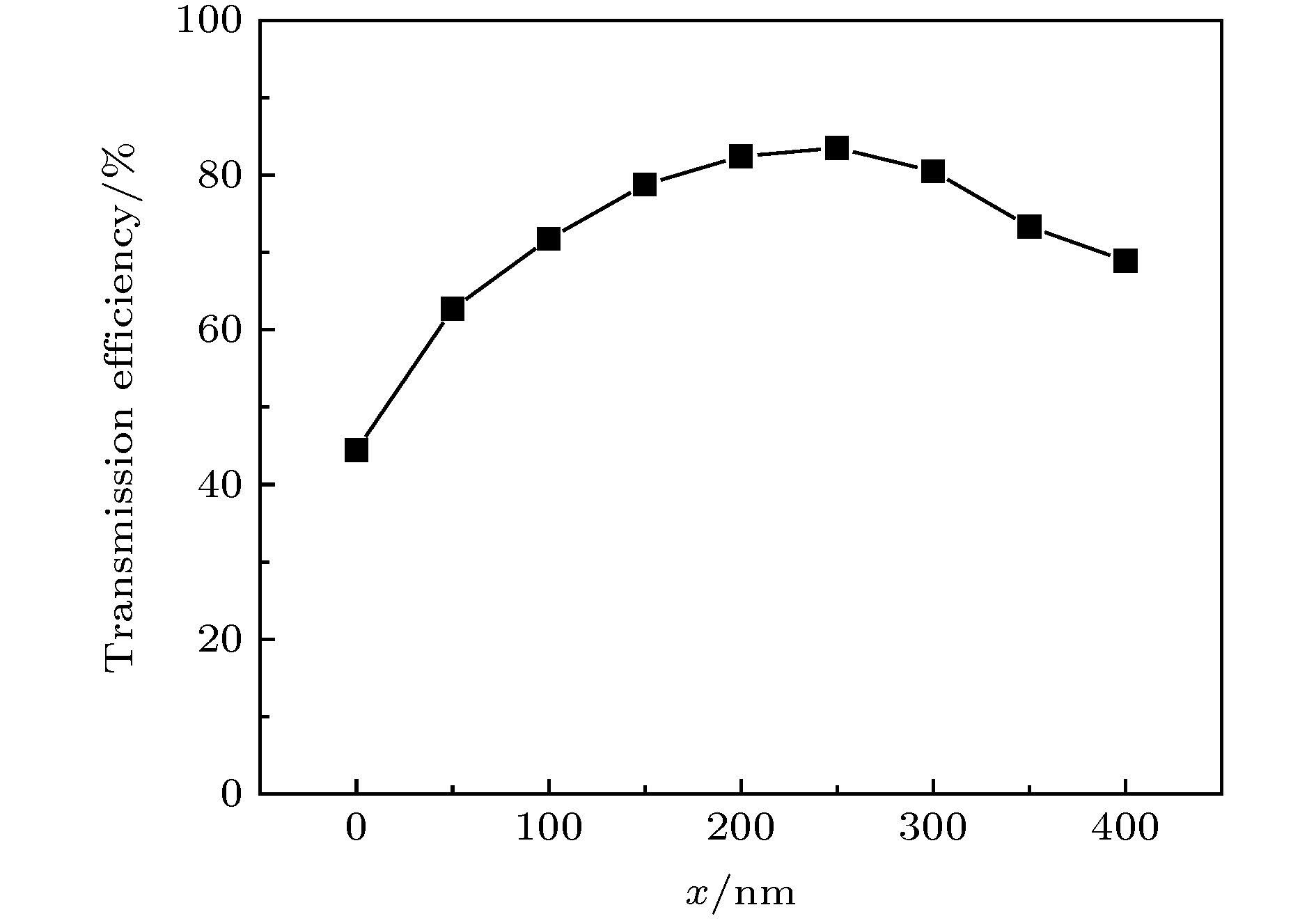 图 6 光经透镜后在波导中的传播效率
 图 7 纳米柱结构与800 nm场幅值分布 (a) 三角形结构; (b) 菱形结构; (c) 圆形结构; (d) 三角形结构场幅值分布; (e) 菱形结构场幅值分布; (f) 圆形结构场幅值分布
 图 8 聚焦效率 (a) 三角形结构; (b) 菱形结构; (c) 圆形结构
 图 9 (a)聚焦光的波导耦合输出; (b)光经透镜后在波导中的传播效率