1.Key Laboratory of Instrumentation Science and Dynamic Measurement, Ministry of Education, North University of China, Taiyuan 030051, China 2.School of Mechanical and Electrical Engineering, Xi’an University of Architecture and Technology, Xi’an 710311, China 3.Shaanxi Key Laboratory of Nanomaterials and Technology, Xi’an 710311, China
Fund Project:Project supported by the National Key R&D Program of China (Grant No. 2017YFB0503100), the China Postdoctoral Innovative Talents Support Program (Grant No. BX20180276), the National Natural Science Foundation of China (Grant Nos. 51805493, 51922009, 51727808, 51775522), the China Postdoctoral Science Foundation (Grant No. 2018M641684), the Applied Basic Research Program in Shanxi Province, China (Grant Nos. 201801D221202, 201901D111011(ZD), 201801D121164), the Key R&D Program in Shanxi Province, China (Grant No. 201803D121067), the Key Laboratory Project Fund (Grant Nos. 6142001180410, 6142001180409), the Key Laboratory of Shanxi Province, China (Grant No. 201905D121001), the Foundation for Young Academic Leaders of North University of China (Grant No. QX201901), and the Shanxi “1331Project”, China.
Received Date:20 May 2020
Accepted Date:26 June 2020
Available Online:27 November 2020
Published Online:05 December 2020
Abstract: Due to the power instability and field non-uniformity of radio frequency (RF), microwave (MW) and laser signals, inhomogeneous broadening of spin magnetic resonance line causes the absorption to decrease in a nuclear resonance system, which can reduce the sensitivity of spin-based sensing and testing technology. In this paper, we propose and design a double solenoid coil RF resonance antenna structure. The nearly uniform RF field density is produced by the two solenoid coil antenna structures that are parallel to the symmetry axis. The size of the uniformity in the center region of double solenoid coil RF resonance antenna structure is about π×375 mm2 × 10 mm. And the non-uniformity is less than 0.9%. Comparing with a single straight wire antenna and the single solenoid coil RF resonance antenna structure, the uniformity is improved by about 56.889 times and 42.889 times, respectively. At the same time, based on the near-field mutual inductance coupled resonance effect, the intensities of RF field in the center region of the two-solenoid coil antenna structure is enhanced. Comparing with the single solenoid coil antenna structures, it is enhanced by about 1.587 times. And the equivalent sensitivity of the silicon vacancy color center spin based sensor is enhanced by about 4.833 times. In the experiment, an optical detection magnetic resonance measurement system based on the spin magnetic resonance effect of silicon vacancy color center in single crystal SiC is built. Comparing with the single straight wire antenna and the single solenoid coil RF resonance antenna structure, the contrast of the silicon vacancy color center spin magnetic resonance signals of the double solenoid coil RF resonance antenna structure increases about 6 times and 2.4 times, respectively. The sensitivity of the spin-based sensor is increased by 4.833 times and 2.071 times through using the modulation and demodulation method, and the noise decreases by 8 times and twice. Hence, based on this double solenoid coil RF resonance antenna structure, the sensitivity of the silicon vacancy spin sensor can be improved. Combined with chip manufacturing technology of SiC wafer, it proves to be a potential approach to developing the high precision, chip scale spin sensor devices and measurement technology. Keywords:silicon vacancy color center/ RF resonant antenna/ uniform field/ spin sensing/ sensitivity
全文HTML
--> --> --> 1.引 言近年来, 碳化硅硅空位色心自旋量子功能结构, 由于其室温下自旋相干时间长、光学泵浦与探测方法简单, 且兼容碳化硅晶圆加工工艺成熟、易于光电器件集成等特性[1-5], 在量子传感与精密测量、量子计算、量子通信等领域展现出了极为广阔的应用前景[6-12]. 目前, 基于碳化硅硅空位色心自旋量子特性的传感与测量技术在单光子源、分子扭矩测量、细胞温度环境监测、磁强计等领域得到了广泛应用[13-18], 且测量精度不断突破传统测量技术精度极限, 成为未来固体量子传感与测量技术发展的主要方向之一[19,20], 然而受限于射频/微波、激光等功率非均匀展宽与波动噪声影响, 导致自旋退相干时间短, 测量精度难以达到理论测量极限[21,22]. 目前常用的射频天线结构主要采用单根直导线结构, 该结构的射频场以直导线为中心向外辐射, 无法构建射频场均匀区[23]. 而应用于微波领域的微波腔均匀天线结构, 由于射频信号波长长, 导致均匀天线结构尺寸达到100 cm2, 限制了SiC自旋功能结构的应用领域[24]. 本文针对SiC基自旋传感测量技术对射频均匀场的需求, 提出设计了一种基于双螺线圈平行对称结构的射频共振增强天线结构(简称双螺线圈共振天线double helical coil resonant antenna, DHCRA). 通过仿真模拟计算, 设计的螺线圈结构的中心频率为70 MHz, 辐射强度为73 A/m, 通过构建双螺线圈平行对称结构, 天线的辐射强度增大了1.587倍, 且均匀区达到π × 375 mm2 × 10 mm, 相比单根直导线结构均匀性提高了56.889倍. 最后通过应用到SiC硅空位色心自旋测量系统中, 得到该结构使得传感测量灵敏度提升了4.833倍, 为高灵敏度自旋传感测量技术提供了技术支撑. 2.天线设计与制造本文基于对称偶极子天线理论与单螺旋天线理论, 设计了双螺线圈平行对称共振射频天线结构, 基于理论公式分析计算[25-29], 通过电磁仿真软件HFSS进行优化, 最后得到如图1(a)所示的三维结构, 通过优化线圈的结构尺寸参数得到最优的结构参数如图1(b)所示. 图 1 (a) DHCRA结构示意图, 红色部分为碳化硅样品, 黄色部分为天线, 绿色部分为碳化硅硅空位色心激发用的红光730 nm激光器, 色心发出的光为红外890—1000 nm; (b) DHCRA设计参数: 天线铜线线宽d = 0.4 mm, 天线铜线线间距w = 0.73 mm, 天线铜线厚度t = 0.035 mm, 双天线之间的距离s = 10 mm, 输入接口线宽d1 = 0.67 mm, d2 = 1.2 mm Figure1. (a) Schematic diagram of double helical coil resonant antenna, the red part is the silicon carbide sample, the yellow part is the antenna, the green part is the red light 730 nm laser used for the excitation of the vacancy color center of silicon carbide silicon, the light emitted by the color center is infrared 890?1000 nm; (b) spiral antenna design parameters: antenna copper wire width d = 0.4 mm, antenna copper wire spacing w = 0.73 mm, antenna copper wire thickness t = 0.035 mm, distance between dual antennas s = 10 mm, input interface line width d1 = 0.67 mm, d2 = 1.2 mm.
通过软件进行磁场仿真, 可以得到在X-Z截面模拟的磁场B示意图, 如图2(a)所示. 可以看出磁场B主要集中分布在沿着Z轴方向两侧的均匀区, 因此, 可以将碳化硅色心结构放置在双螺旋天线两侧的均匀区, 有效降低自旋磁共振效应的非均匀展宽问题. 在图1(b)的实验参数基础上, DHCRA天线的S11参数即回波损耗的电磁仿真结果与实验测试结果如图2(b)所示. 经过HFSS参数化扫描结果分析, 得到最优的回波损耗信号, 本文设计的天线结构在70 MHz的回波损耗最优可以达到–33 dB. 由于DHCRA的辐射功率与阻抗有关系, 因此, 在DHCRA之间接入50 Ω匹配阻抗来提高射频信号的辐射效率. 图 2 (a)本文设计的天线结构的X-Z平面磁场分布图; (b) DHCRA结构的S11仿真结果与测试结果. 插图为DHCRA的实物照片 Figure2. (a) Magnetic field distribution in the X-Z plane of our antenna structure; (b) simulation results and measurement results of the parameter S11 of the DHCRA structure. The inset shows the physical photograph of DHCRA.
通过测试得到谐振频率实际测试结果与仿真结果相差约5 MHz, 主要原因包括: 1)受限于加工工艺精度, 射频天线的金属线条的直径、线圈长度、线条间隔、线圈整体直径难以完全与仿真尺寸一致; 2)基材材质的介电常数、电阻率等参数采用理想模型, 与实际有差异; 3)当两个线圈之间的间隔在0.4—15.0 mm之间时谐振峰位置基本不变, 只影响回波损耗值, 当间距小于0.4 mm, 谐振频率与线圈间距成反比; 4)测试环境的温湿度引起的线条热胀冷缩(通常情况下较小, 可以忽略); 5)测试时测量尾线的长度和弯曲形变(可改变尾线的长度和形变来控制螺线圈的谐振频率). 图3(a)与图3(b) 为输入70 MHz信号时, DHCRA结构的两个截面的场强B分布结构图. 从图中可以看到, DHCRA沿着Z轴的场强B分布均匀, 靠近Z轴两侧虚线框的部分场强分布较为集中. 根据非均匀性定义和标准计算方法, 通过提取图3(a),(b)虚线框内场强幅值点的最大值与最小值作差, 随后与平均场强做除法计算, 得到X-Z平面两侧的均匀区的非均匀度约为0.9%, X-Y平面环形均匀区的非均匀度约为0.78%, 两侧均匀区非均匀度平均约为0.9%. 图 3 (a) 70 MHz下X-Z平面的场强仿真分布图(图中的$\varepsilon $为非均匀度); (b) 70 MHz下的X-Y平面的场强仿真分布图; (c) 70 MHz下的均匀区(X = 14.86 mm)Z轴方向场强仿真曲线图; (d) 70 MHz下X轴方向的场强仿真曲线图 Figure3. (a) Simulated distribution of the magnetic field in the X-Z plane at 70 MHz (In the figure $\varepsilon $is the non-uniformity); (b) simulated distribution of magnetic field in the X-Y plane at 70 MHz; (c) simulation curve of magnetic field in the X-axis direction at 70 MHz; (d) simulation curve of magnetic field in the Z-axis direction of the uniform zone (X = 14.68 mm) at 70 MHz.
在仿真过程中, 对于X-Z平面两侧的均匀区, 当线圈间距在0.4—20.0 mm之间时, 随着两线圈间距的增加非均匀度不断提高. 当线圈间距超过20 mm后由于场强大幅度减弱, 随着间距扩大非均匀度不断降低, 而非均匀度的线圈间距与线圈线条宽度对该平面非均匀性几乎无影响. 对于X-Y平面的环形均匀区, 当线圈线条间距与宽度之和固定时, 随着线宽的增加非均匀度不断减小, 而两线圈间距对该平面非均匀性无影响. 研究中将DHCRA天线结构中间部分设为中心, 以沿着中心的X轴为横坐标, 场强大小为纵坐标进行取点分析得到如图3(d)所示的场强分布图. 根据图3(d)得到X轴上均匀区的最大场强位于+14.68与–14.2 mm处, 取正向X = 14.68进行Z轴曲线绘制得到如图3(c)所示分布图. 可以看到沿着Z轴分布的中间区域为最大值, 辐射强度最大, 而由图3(d)可以看出沿着X轴的两侧各具有一个最值点. 同时, 由于待激发的碳化硅样品不与线圈结构相接触, 所以线圈工作产生的热量不会直接传到碳化硅样品, 从而有效隔离了线圈产生热量的干扰. 为了进一步研究样品结构对天线结构的非均匀性影响, 通过仿真研究了DHCRA天线结构加入碳化硅样品前后的场强分布特性, 结果如图4所示. 可以看出, 加入样品前后射频天线结构中场强的分布基本无变化, 因此, 碳化硅样品对所设计天线结构的非均匀性无影响, 为高可靠的SiC基传感与测量结构研制提供技术支撑. 图 4 (a)未加入样品时X-Z平面磁场仿真分布图; (b)加入碳化硅样品后X-Z磁场仿真分布图 Figure4. (a) Simulation distribution of X-Z plane magnetic field without adding samples; (b) X-Z magnetic field simulation distribution after adding silicon carbide sample.
3.不同天线结构性能测试为了对比目前碳化硅硅空位自旋结构常用射频天线结构, 对比了单导线(single copper antenna, SCA), 单线圈(single loop antenna, SLA)和DHCRA三种不同天线结构的射频信号辐射强度, 如图5所示. 在相同比例下得到DHCRA结构虚线区域的均匀场场强更大, 而SLA与SCA结构分布较为分散且强度较低. 而且, 相比于SCA与SLA结构, DHCRA结构的均匀性分别提高了55.889倍与42.889倍, 场强分别提升1.587倍与1.177倍, 极大地增强了射频信号辐射的均匀性与强度, 为高灵敏度的碳化硅硅空位色心自旋基传感和测量方法提供了研究基础. 图 5 (a) SCA, SLA与DHCRA的三维结构示意图; (b)三种结构磁场强度仿真分析图与非均匀度参数示意图 Figure5. (a) Three-dimensional structure diagram of SCA, SLA and DHCRA; (b) three kinds of structure magnetic field strength simulation analysis diagram and non-uniformity parameter diagram.
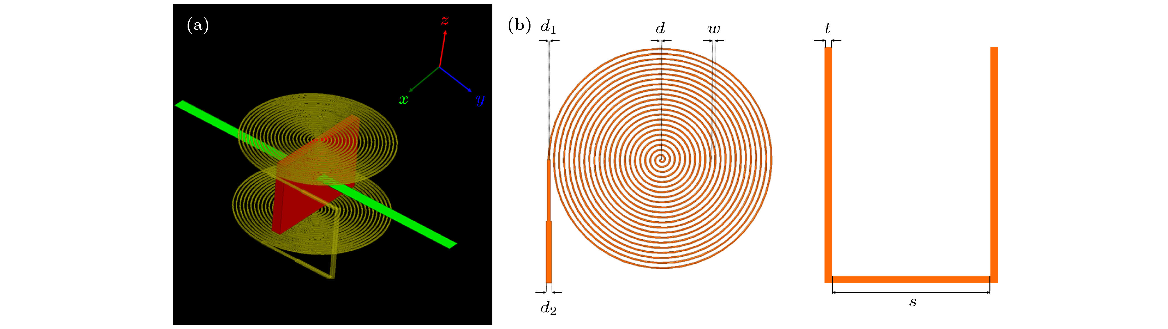 图 1 (a) DHCRA结构示意图, 红色部分为碳化硅样品, 黄色部分为天线, 绿色部分为碳化硅硅空位色心激发用的红光730 nm激光器, 色心发出的光为红外890—1000 nm; (b) DHCRA设计参数: 天线铜线线宽d = 0.4 mm, 天线铜线线间距w = 0.73 mm, 天线铜线厚度t = 0.035 mm, 双天线之间的距离s = 10 mm, 输入接口线宽d1 = 0.67 mm, d2 = 1.2 mm
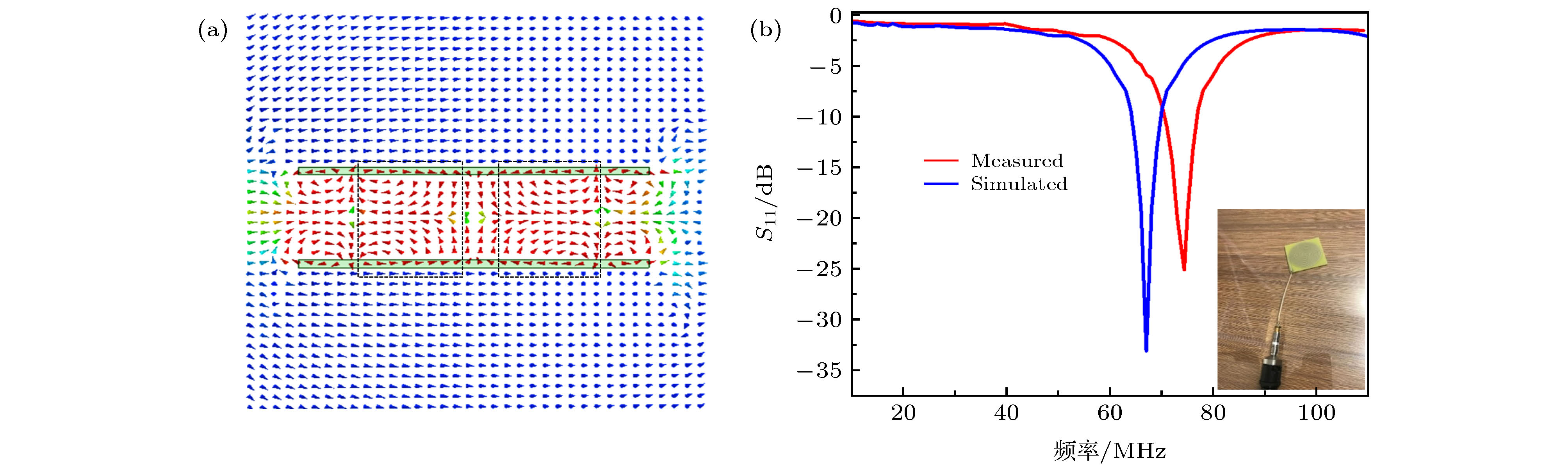 图 2 (a)本文设计的天线结构的X-Z平面磁场分布图; (b) DHCRA结构的S11仿真结果与测试结果. 插图为DHCRA的实物照片
 图 3 (a) 70 MHz下X-Z平面的场强仿真分布图(图中的

 图 4 (a)未加入样品时X-Z平面磁场仿真分布图; (b)加入碳化硅样品后X-Z磁场仿真分布图
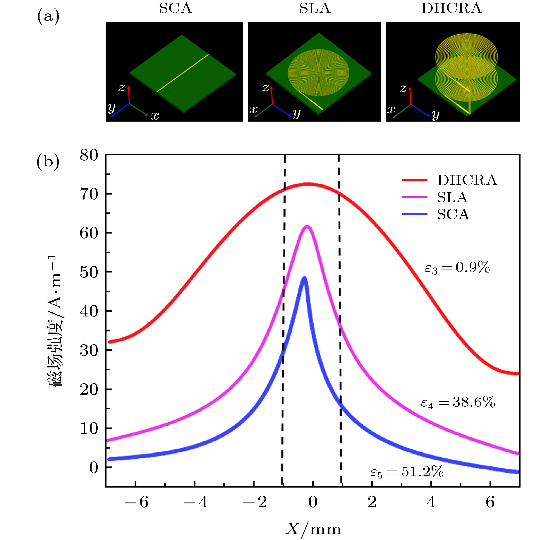 图 5 (a) SCA, SLA与DHCRA的三维结构示意图; (b)三种结构磁场强度仿真分析图与非均匀度参数示意图


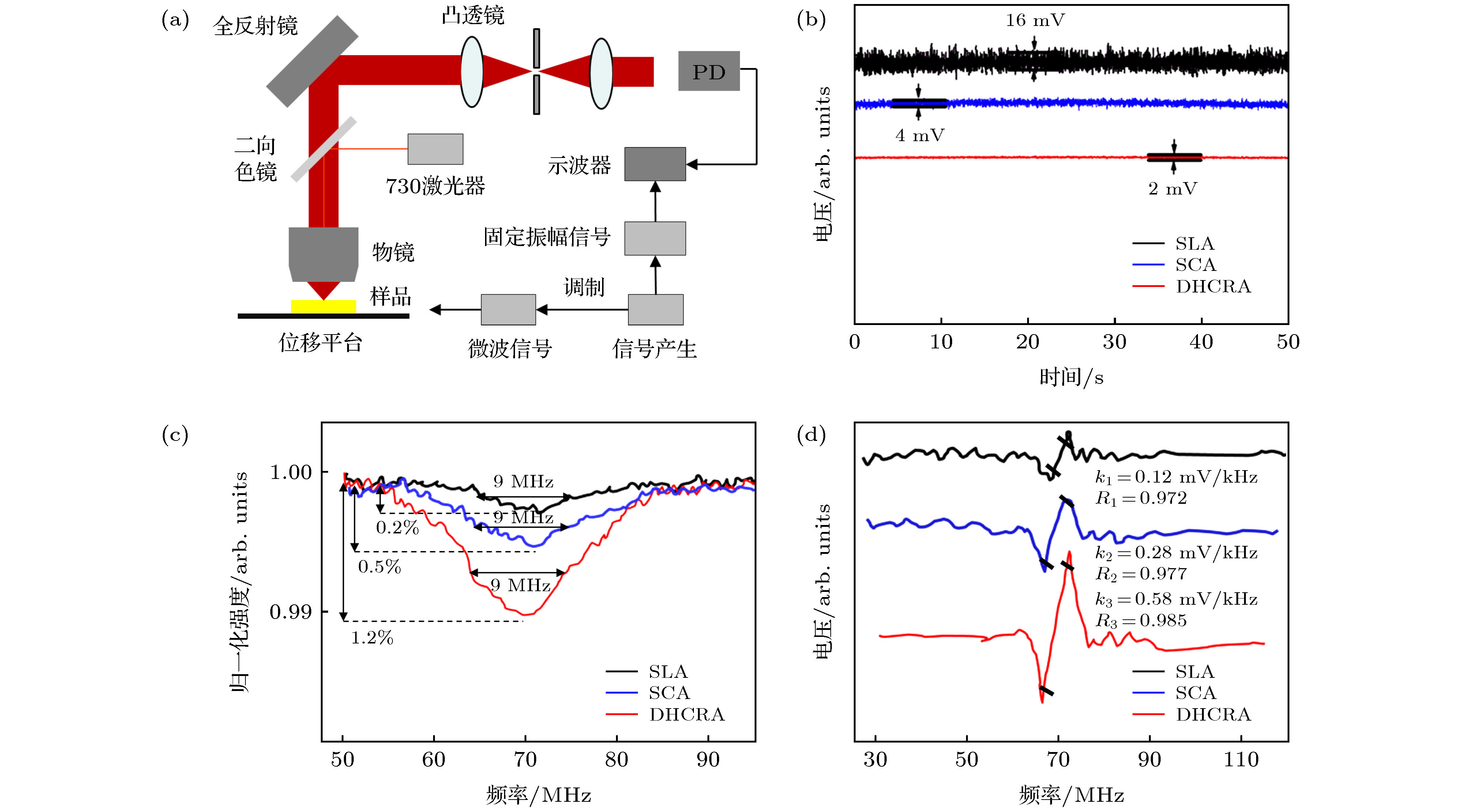 图 6 (a)光学检测共振光路与频率调制系统; (b)三种结构的光学检测共振谱分布; (c) 70 MHz共振频率下三种结构的噪声波动图; (d) 三种结构的解调测试结果图


