Fund Project:Project supported by the National Natural Science Foundation of China (Grant Nos. 11847002, 11904008), the China Postdoctoral Science Foundation (Grant No. 2019M662132), and the Natural Science Foundation of Anhui Province, China (Grant No. 1908085QA21)
Received Date:08 April 2020
Accepted Date:18 July 2020
Available Online:26 November 2020
Published Online:05 December 2020
Abstract:Mirrors can be seen everywhere in daily life and play an important role in modern optical systems. A traditional mirror, which is made of noble metals, usually has a zero electric field strength and maximal magnetic field strength at its surface induced by the out-of-phase of electric field and in-of-phase of magnetic field between the reflected field and incident field due to the boundary condition of perfect electric conductor. As the magnitude of local electric field determines the strength of the light-matter interaction, it is clear that this interaction is suppressed near the mirror surface. Magnetic mirror, which can enhance electric field on the surface, has been widely applied to strong light-matter interaction for biological sensing, material analysis, and imaging. However, the conventional smooth magnetic mirror with a plane surface is difficult to induce sufficient light-matter interaction when the matter has a complex geometrical shape. Here in this work, we propose a concept of magnetic mirror with a rough interface designed by an array of artificial surface plasmonic structures. The artificial surface plasmonic structure on a subwavelength scale is designed by periodically inserting spiral metallic strips into a dielectric cylinder to support the strong magnetic dipolar resonant mode. The magnetic dipolar resonance of the excited structure is induced by the displacement current circle. Therefore, the resonant frequency is related to the geometrical parameters of the helical structure closely. When we reduce the outer radius of the structure, the magnitude of the displacement current circle will change, resulting in blue-shift of the resonant frequency. At the same time, we also find that increasing the spiral degree of the structure will cause the magnetic dipolar resonance frequency to become red-shifted. Particularly, the same magnetic dipolar mode can be supported in a spiral structure of different size by tuning the spiral degree accordingly. In this context, we design a rough magnetic mirror constructed by the artificial surface plasmonic structures with various sizes, and demonstrate that the efficiency of rough magnetic mirror is in agreement with that of smooth magnetic mirror. The proposed rough magnetic mirror can provide the unique ability to enhance the interaction between light and complicated matter for the application of biological sensing and imaging in microwave and terahertz band. Keywords:rough magnetic mirror/ spoof surface plasmonic structure/ light-matter interaction
2.人工表面等离激元结构设计及其电磁响应图1(a)显示了二维的人工表面等离激元结构, 该螺旋结构可通过周期地将具有对数螺旋线的螺旋金属条插入到介电圆盘中来构造. 在该模型中, 空心螺旋结构的内半径和外半径分别用r和R表示. 此处, (ρ, θ)是极坐标, a和d = 2πR/N分别对应于金属条的宽度和周期, 其中N是金属条的数量. 结构中蓝色部分选择了一种折射率ng为3.4的材料(类似于硅), 黄色部分代表完美电导体, 整个结构被置于空气之中. 这种类似的螺旋结构已经被提出用来分析描述人工表面等离激元的电磁特性[28]. 在这里, 对数螺旋线的公式可以写成$\rho = r \exp \left[ {\left( {{\rm{lo}}{{\rm{g}}_{10}}\left( {R/r} \right)/{\theta _0}} \right)\theta } \right]$, 螺旋槽的长度写为 图 1 (a)人工表面等离激元结构示意图; (b)计算的由不同材料构成的人工表面等离激元结构的散射谱, 其中黑色曲线代表PEC, 蓝色曲线代表Ag, 红色曲线代表Cu; (c)图1(b)中的黑色实线对应的共振峰的近场模式Hz Figure1. (a) Schematic diagram of spoof surface plasmonic structure; (b)calculated scattering cross section spectrum of spoof surface plasmonic structure made of different materials, where the black curve represents PEC, the blue curve represents Ag and the red curve represents Cu; (c) near-field pattern ${H}_{ {z}}$ for the resonant peak in the black solid line of (b).
其中$ {\theta }_{0} $是对应于螺旋槽长度L的旋转角度, 在下文中$ {\theta }_{0} $表示结构的螺旋度. 这些结构参数在图1(a)中已经标示. 这里, 选取的结构参数为R = 45 μm, r = 5 μm, a = d/3, N = 4, ng = 3.4, $ {\theta }_{0} $=1.5π. 由于a <$d\ll{\lambda }_{0}$, 结构的大小可以被设计在深亚波长范围内, 其中λ0是入射波的波长. 为了研究这种螺旋结构中的光学响应特性, 使用一个沿y方向传播的横磁平面波入射该螺旋结构. 在图1(b)中, 使用商用软件COMSOL MULTIPHYSICS计算了半径为R的螺旋结构的归一化散射截面, 这里的归一化散射截面为计算的总散射截面除以直径2R. 由于金属在较低频率下的行为类似于完美电导体, 在这里首先将人工表面等离激元结构的材料假定为完美电导体, 并计算了其散射截面(图1(b)中黑线). 另外从实际实验考虑, 还在图1(b)中给出了由实际金属银和铜材料制成的人工表面等离激元结构的归一化散射截面, 并分别用蓝色和红色实线表示. 从图1(b) 可以发现, 在结构的散射谱中有一个频率为f = 0.2684 THz的共振峰. 为了进一步确认这些共振峰的模式, 给出了该频率下结构的近场分布Hz, 如图1(c)所示, 可以发现该共振峰对应着磁偶极模式. 接下来, 将讨论结构参数对磁偶极子谐振频率的影响. 图2 (a)中的绿色实曲线显示了当R = 45 μm并且其他结构参数不变时, 随着结构螺旋度从π增加到3π时谐振频率的变化, 此时可以发现谐振频率是下降的. 此外, 也发现当R从45 μm依次降到15 μm时, 对应于磁偶极子模式的谐振频率发生了蓝移. 产生这种现象的原因是结构参数的变化影响位移电流圆的大小, 从而导致磁偶极子共振频率的偏移. 同样, 在图2(b)和图2(c)中也研究了对于不同的内半径r与a/d的情况下, 磁偶极子模式的谐振频率与螺旋度之间的关系. 这些结果表明, 可以通过裁剪结构几何参数自由地调整与结构中磁偶极子相关的共振响应. 图 2 (a)不同外半径下, 磁偶极子共振频率与螺旋度的关系, 图中的虚线和4条实线的交点代表对应于相同共振频率的4种结构; (b)不同内半径下, 磁偶极子共振频率与螺旋度的关系; (c) 对于不同的a/d, 磁偶极子共振频率与螺旋度的关系 Figure2. (a) The magnetic dipole resonance frequency as the function of spiral degree for different outside radii. The intersection of the horizontal dotted line and the four solid curves in the figure represent the four structures corresponding to the same resonance frequency; (b) the relationship between the resonance frequency of magnetic dipole and spiral degree at different inner radii; (c) for different a/d, the relationship between the resonance frequency of magnetic dipole and spiral degree.
3.基于人工表面等离激元结构的平面磁镜在上面的研究中, 主要讨论了人工表面等离激元结构的电磁响应特性, 结果表明, 该结构具有强磁偶极共振响应, 并且其共振频率可以方便地通过结构参数调控. 接下来, 将讨论如何通过人工表面等离激元结构阵列实现磁镜功能. 作为参考, 首先计算了平面波入射的完美电导体和完美磁导体产生的空间场分布(图3(a), (b)). 通过比较两图, 不难发现在完美电导体表面具有零电场强度, 但在完美磁导体表面却产生最大电场强度. 显然, 在完美磁导体界面处驻波的波节和波腹位置与完美电导体表面处的相比偏移了Δy ≈ λ/4, 也就是说二者之间近似相差π/2的相位. 图 3 具有 (a)理想PEC和(b)理想PMC边界壁的电场|E|的分布; (c)?(f)在图2中用“1” “2” “3”和“4”表示的4种结构的电场|E|的分布; (g)?(h) 对于(c)中的结构参数, 用不同材料制成的结构的透射谱和反射谱 Figure3. Snapshots of the electric field |E| for boundary walls with (a) the ideal PEC and (b) the ideal PMC; (c)?(f) snapshots of the electric field |E| for four structures of Fig. 2 denoted by “1” “2” “3” and “4”; (g)?(h) for the structural parameters of (c), transmission and reflection spectrum of structures made of different materials.
接下来, 将使用人工表面等离激元结构来演示所提出的磁镜. 图3(c)展示出了沿y方向的磁镜(R = 45 um, r = 5 um, a/d = 1/3, N = 4, $ {\theta }_{0} $ = 2π)的电场大小分布. 图3(a)—(c)中给出的观测尺寸为700 μm × 2180 μm, 并且在x方向设置为周期性边界条件. 研究发现在结构表面产生了最大电场. 这一结果显然支持了本研究组的想法以及磁镜模型的有效性. 另外, 类似纳米结构(如蝴蝶结结构)缝隙的近场增强效应[29-31]也可以增强表面电场, 但是, 用来增强电场的纳米结构通常需要在底部设置一层基板(例如玻璃、石英、蓝宝石或硅)来制造, 因为独立的纳米间隙在结构上是很脆弱的. 其次, 相比纳米结构缝隙的近场增强效应, 这种螺旋结构在共振频率的调节上具有很大的自由度并且可以在深度亚波长下操纵光. 磁镜可以有效消除常规介质界面处存在的电场的半波损耗, 从而使电场在边界附近增强. 由于它的这个优点, 磁镜被广泛运用于现代光学系统中. 为了实现小型化以便于集成和减少耗材, 需要寻找具有同样功能的超薄磁镜. 另外, 图2(a)中的结果表明能通过增加结构的螺旋度将具有相同谐振频率的磁偶极子支持在更小的外半径的螺旋结构中. 如图2(a)所示, 可以清楚地看到4个不同的交点, 这些交点分别对应于不同结构的磁镜. 接下来, 依次将这4种不同结构的磁镜绘制出来. 首先, 图3(c)展示出了沿y方向的磁镜(R = 45 μm, r = 5 μm, a/d = 1/3, N = 4, $ {\theta }_{0} $ = 2π)的电场大小分布. 然后, 将外半径减小到R = 35 μm, 同时将螺旋度增加到2.3π, 并在图3(d)中绘制出对应结构的电场. 接下来, 给出与第三个点相对应的场分布. 此时, 在图3(e)中, 外半径减小到了25 μm, 螺旋度增大到了2.62π. 最后, 如图3(f)所示, 将结构的外半径调整为15 μm, 将螺旋度增大到2.89π. 图4(c)—(f)显示了x-y平面上电场的近场分布. 从这些场分布中, 不难发现这些结构的模式分布是一致的, 并且这些磁镜的光谱分布也非常一致. 综上可得, 本研究组实现了具有相同功能的超薄磁镜, 为实现光学仪器的小型化集成和减少耗材提供了一种潜在的可能. 图 4 (a), (b)不同大小的光滑磁镜的电场|E|的分布及其局部放大图; (c)与(a)和(b)相同, 只是用粗糙的磁镜代替光滑的磁镜 Figure4. (a), (b) Snapshots of the electric field |E| for smooth magnetic mirror of different sizes and their enlarged views; (c) same as (a) and (b) except replacing smooth magnetic mirror by rough magnetic mirror.

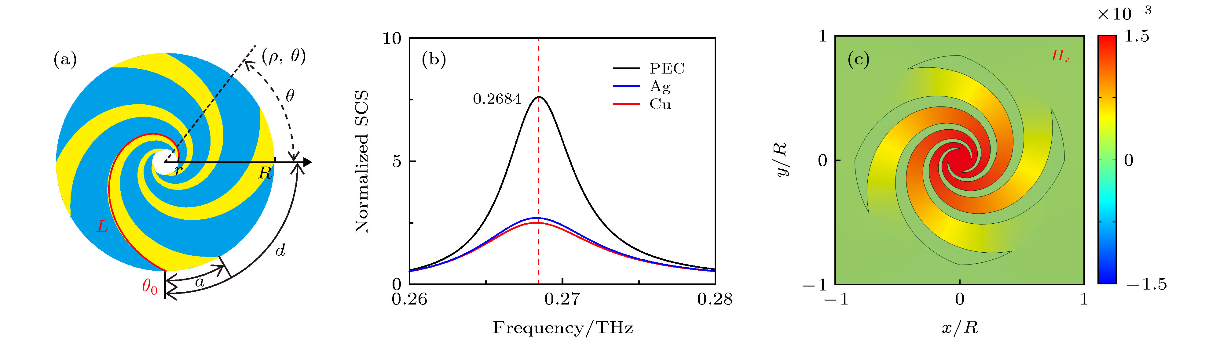 图 1 (a)人工表面等离激元结构示意图; (b)计算的由不同材料构成的人工表面等离激元结构的散射谱, 其中黑色曲线代表PEC, 蓝色曲线代表Ag, 红色曲线代表Cu; (c)图1(b)中的黑色实线对应的共振峰的近场模式Hz


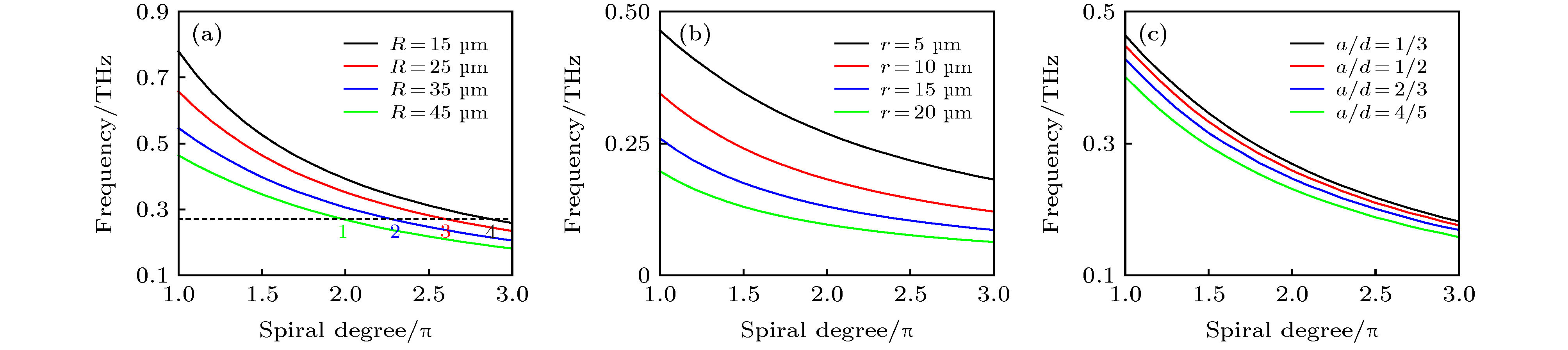 图 2 (a)不同外半径下, 磁偶极子共振频率与螺旋度的关系, 图中的虚线和4条实线的交点代表对应于相同共振频率的4种结构; (b)不同内半径下, 磁偶极子共振频率与螺旋度的关系; (c) 对于不同的a/d, 磁偶极子共振频率与螺旋度的关系
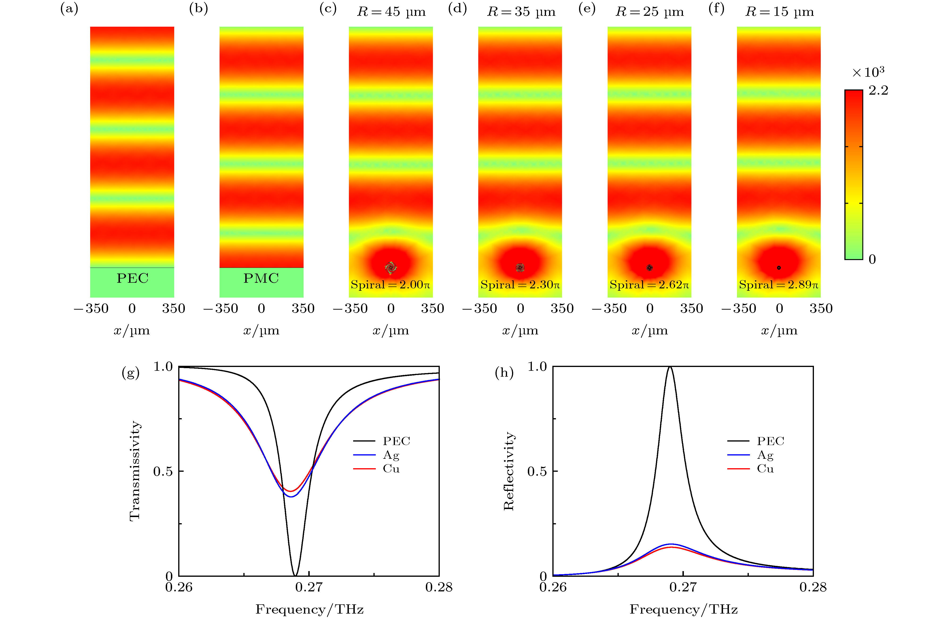 图 3 具有 (a)理想PEC和(b)理想PMC边界壁的电场|E|的分布; (c)?(f)在图2中用“1” “2” “3”和“4”表示的4种结构的电场|E|的分布; (g)?(h) 对于(c)中的结构参数, 用不同材料制成的结构的透射谱和反射谱

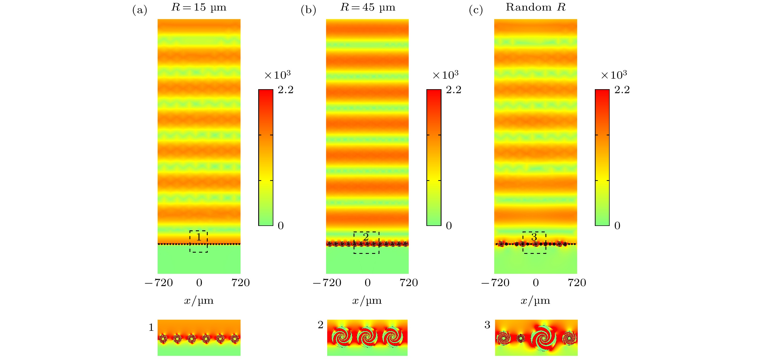 图 4 (a), (b)不同大小的光滑磁镜的电场|E|的分布及其局部放大图; (c)与(a)和(b)相同, 只是用粗糙的磁镜代替光滑的磁镜


