Abstract: With the development of the application of AlGaN/GaN high electron mobility transistors in the radio frequency field, a capacitance model that can accurately describe the C-V characteristics of the device has become an important research topic. The gate capacitance of GaN HEMT can be divided into two parts: intrinsic capacitance and fringing capacitance related to two-dimensional electronic gas (2DEG) electrode. The fringing capacitance plays an important part in the switching device. The outer fringing capacitance Cofs/d dominates the fringing capacitance and is affected by the bias applied, especially the drain outer fringing capacitance Cofd. In order to establish the Cofd model which is related to the bias condition, the physics-based model of Cofd is established based on the conformal mapping, including the drain channel length variable. Since the drain channel length is related to the bias applied, the channel length modulation effect can be used to study how bias apllied effect the channel, and the relationship between Cofd and the bias condition is obtained. In addition, the threshold voltage variable is introduced when the channel length modulation effect is considered, and the threshold voltage drift caused by changes in the internal parameters and temperature of the device is studied using the threshold voltage variable in the model, and the relationship between Cofd and threshold voltage and temperature under different bias was obtained. It is found from the results of the study that as drain bias increases from zero, the channel length modulation effect keeps Cofd unchanged at lower drain bias. When the drain bias continues to increase, Cofd begins to decay again, and its decay rate slows down with the increase of gate bias. The decrease of donor impurity concentration and Al component in AlGaN barrier layer may increase the threshold voltage, which will strengthen the channel length modulation effect on Cofd, resulting in linear attenuation of Cofd. With the increasing of drain bias, the influence of threshold voltage shift on Cofd is enhanced, and the change of device operating temperature will enhance the threshold voltage shift and cause the deviation of Cofd. Moreover, with the continuous increase of drain bias, Cofd becomes more sensitive to the temperature variation. Keywords:HEMT/ outer fringing capacitances/ channel length modulation effect/ model
全文HTML
--> --> --> 1.引 言AlGaN/GaN高电子迁移率晶体管(high electron mobility transistor, HEMT)具有良好的高频和高功率特性, 在射频领域得到了广泛的关注[1,2]. GaN HEMT的C-V特性是器件的一个重要参数. 其栅极电容可以分为本征电容和二维电子气(two-dimensional electron gas, 2DEG)电极边缘电容两部分, 而边缘电容在总的栅极电容中占有相当大的比例, 器件正常工作状态下占10%以上, 在弱反型或截止区时甚至达到90%[3]. 边缘电容包括内部边缘电容Cifs/d和外部边缘电容Cofs/d, 其中Cofs/d会受到外部偏置的影响, 特别是漏端一侧的外部边缘电容Cofd所受的影响尤为明显. Pregaldiny等[4]曾指出LDD MOSFET内部边缘电容Cifs/d与器件所施加的栅极电压密切相关, 建立了Cifs/d对应的物理模型. Bansal等[5]利用保角映射法对DGMOS的外部边缘电容Cofs/d进行了物理建模, 该Cofs/d模型中的变量由工艺参数决定, 未考虑外加偏压对Cofs/d的影响. 之后, Zhang等[3]推导了GaN HEMT包含边缘电容Cifs/d和Cofs/d的电容模型, 认为边缘电容对GaN HEMT器件开关特性有着重要的影响. 最近, Li等[6]建立了适用于GaN HEMT边缘电容的电荷模型, 指出外部边缘电容与施加的漏极偏压相关, 之后Jia等[7]对GaN HEMT边缘电容模型进行了改进, 在传统Cofs/d模型前添加指数修正函数来表述Cofd随外加偏压的变化情况. 到目前为止, 由于利用保角映射法推导得到的Cofd模型只与工艺参数相关, 常被当作固定值处理. 而实验发现它会受到外加偏置电压的影响, 但目前已报道的研究文献尚未给出Cofd关于外加偏压的理论解释及相应的物理模型, Cofd关于外加偏压的物理模型有待确立. 本文通过分析外部边缘电容的形成机理, 推导出新的Cofd的核心模型, 同时利用沟道长度调制效应确定漏端沟道长度, 研究了外加偏压、温度变化及阈值电压漂移对Cofd的影响, 建立了相应的Cofd物理模型. 2.物理模型推导GaN HEMT的沟道长度与器件工作状态相关. 以耗尽型GaN HEMT为例, 其关断(OFF)与开启(ON)状态示意图如图1所示. 当Vg低于阈值电压(Vth)时, 器件处于关断状态, 此时Vg太小不足以在AlGaN/GaN形成能供2DEG运动的势阱, 在栅极下方形成一小区域的耗尽区[7], 2DEG沟道被耗尽区隔开为漏端沟道和源端沟道. 同时, 在栅极与漏极之间, 靠近栅极的AlGaN类施主表面陷阱起着“虚栅”的作用[8], 这个能够俘获电子的虚栅使栅极和漏极之间的等效电位(VGD)降低, 把栅极靠近漏端下方的2DEG也耗尽[9], 导致耗尽区向漏端延伸, 漏端沟道长度(Ld)减小; 当Vg足够大且稳定时, HEMT处于开启状态, 栅极下方的耗尽区消失, 同时类施主表面陷阱释放电子, 由虚栅引起的耗尽区也连同消失, 这时漏或源端沟道长度都达到最大值. 图 1 GaN HEMT不同工作状态下外部边缘电容示意图 (a)处于关断状态; (b)处于开启状态 Figure1. Schematic of GaN HEMT outer fringing capacitances in different state: (a) In the OFF-state; (b) in the ON-state.
图2是与Cofd相关电场的示意图, Tg是栅极的厚度, TAlGaN是AlGaN势垒层的厚度, Ldep_d是类施主表面陷阱对2DEG的耗尽长度, Ld是不考虑沟道长度调制效应时的漏端沟道长度. 图 2 栅极侧壁与2DEG之间的电场示意图 Figure2. Schematic of normal electric field between the side wall of the gate and the 2DEG.
共焦后的电场示意图如图3(a)所示, 令Lcd = Ld后电场示意图如图3(b)所示. 图 3 (a)共焦后的电场示意图; (b) Lcd = Ld时的共焦电场 Figure3. (a) Electric field lines after transforming the nonconfocal elliptical system to the confocal system; (b) the confocal system with Lcd = Ld.
表1模型仿真的器件参数值 Table1.Model parameters in this paper.
23.1.Cofd核心模型验证
-->
3.1.Cofd核心模型验证
GaN HEMT从关态转变为开态并处于稳定时, Ldep_d会逐步转变为零. 对Cofd的核心公式(8)式进行仿真, Ldep_d扫描范围设置为0到0.6 μm, 同时把仿真结果与文献[7]的实验数据进行对比, 结果如图5所示, 仿真结果与实验数据有较好的拟合度, 而相比以往的Cofd模型, 本文提出的模型包含了Lcd项, 可进一步研究外加偏压对Cofd的影响. 图 5 2DEG沟道被类施主表面陷阱耗尽的长度对Cofd的影响关系图 Figure5.Cofd versus the extended depletion length induced by donor-like surface traps.
23.2.偏置条件对Cofd的影响 -->
3.2.偏置条件对Cofd的影响
33.2.1.Vdsat与Vg的关系 -->
3.2.1.Vdsat与Vg的关系
由(15)式和(16)式得到的$ E_{\rm f}\text{-}n_{\rm s} $与Vg关系如图6所示, 由图可得当Vg = –3 V时, 已经存在浓度高达1011 cm–2的2DEG, 这些电子主要来源于类施主表面陷阱和AlGaN/GaN的极化效应[15]; 当Vg处于Ⅰ区时, HEMT工作在中反型区[18], Vg增大使势阱加深, 此时由AlGaN/GaN极化效应产生的极化电场EAlGaN较强, 该电场把AlGaN层被表面陷阱俘获的电子和内部杂质电离的价电子扫向势阱[19], 势阱内的电子浓度急剧增加导致Ef往远离导带底部的方向移动, Ef迅速增加; 当Vg处于Ⅱ区时, HEMT工作在强反型区, 此时由AlGaN层扫向势阱的电子已经相对较多, 这些电子与留在AlGaN层的电离施主杂质和表面陷阱共同形成电场E2DEG, 该电场与极化电场EAlGaN方向相反, 抑制2DEG浓度ns的继续增加, 并且随着ns的增加其抑制作用逐渐增强, 导致ns的增量减缓, Ef趋向线性变化. 图 6Vg与2DEG浓度ns和Ef的关系曲线 Figure6. The curve of the density ns of 2DEG and Ef versus Vg
基于该Ef模型得到的Vdsat与Vg关系如图7所示, 结果与实验数据进行对比, 实验数据来源于文献[20]. 分析图7发现, 新Vdsat模型与实测数据拟合度较高, Vdsat与Vg呈微弱的非线性关系, 这是由Ef随Vg的非线性变化引起的, 而准确的Vdsat是分析HEMT沟道调制效应的关键. 图 7Vg与Vdsat的关系曲线 Figure7. The curve of Vdsat versus Vg.
33.2.2.沟道长度调制效应对Cofd的影响 -->
3.2.2.沟道长度调制效应对Cofd的影响
给栅极施加足够大的偏压使HEMT工作在开启状态, Vds变化范围设置为0到60 V, 图8是Cofd与Vds的关系图, 上3条曲线是本文Cofd-Vds的仿真结果, 下3条曲线是在Cofd传统模型前添加修正函数后的仿真结果, 对比模型来源于文献[7]中给出的Cofd-Vds模型. 由新Cofd模型曲线可知: 当Vds < Vdsat时, 由于不存在沟道长度调制效应, Lcd保持在最大值, 此时Cofd不受Vds变化的影响, 对Vg的变化也不敏感; 当Vds ≥ Vdsat且Vds不断增加时, 沟道长度调制效应作用增强, 夹断点不断往源端移动, Cofd因为Lcd的减小而衰减; 当Vg升高时Cofd曲线衰减速率减慢, 这是因为Vg与Vdsat呈非线性正相关关系, Vg的升高会导致Vdsat相应增加, 更高的Vdsat意味着Lcd受沟道长度调制效应调制作用所消耗的Vds变大, Cofd衰减起点被延后, 曲线整体衰减速率减缓. 图 8 传统模型和本文模型得到的Vds与Cofd的关系曲线 Figure8. The curve of Cofd versus Vds obtained from the traditional model and the model in this paper.
 图 1 GaN HEMT不同工作状态下外部边缘电容示意图 (a)处于关断状态; (b)处于开启状态
 图 2 栅极侧壁与2DEG之间的电场示意图
 图 3 (a)共焦后的电场示意图; (b) Lcd = Ld时的共焦电场
 图 4 Lcd = Ld所引入的误差


 图 5 2DEG沟道被类施主表面陷阱耗尽的长度对Cofd的影响关系图
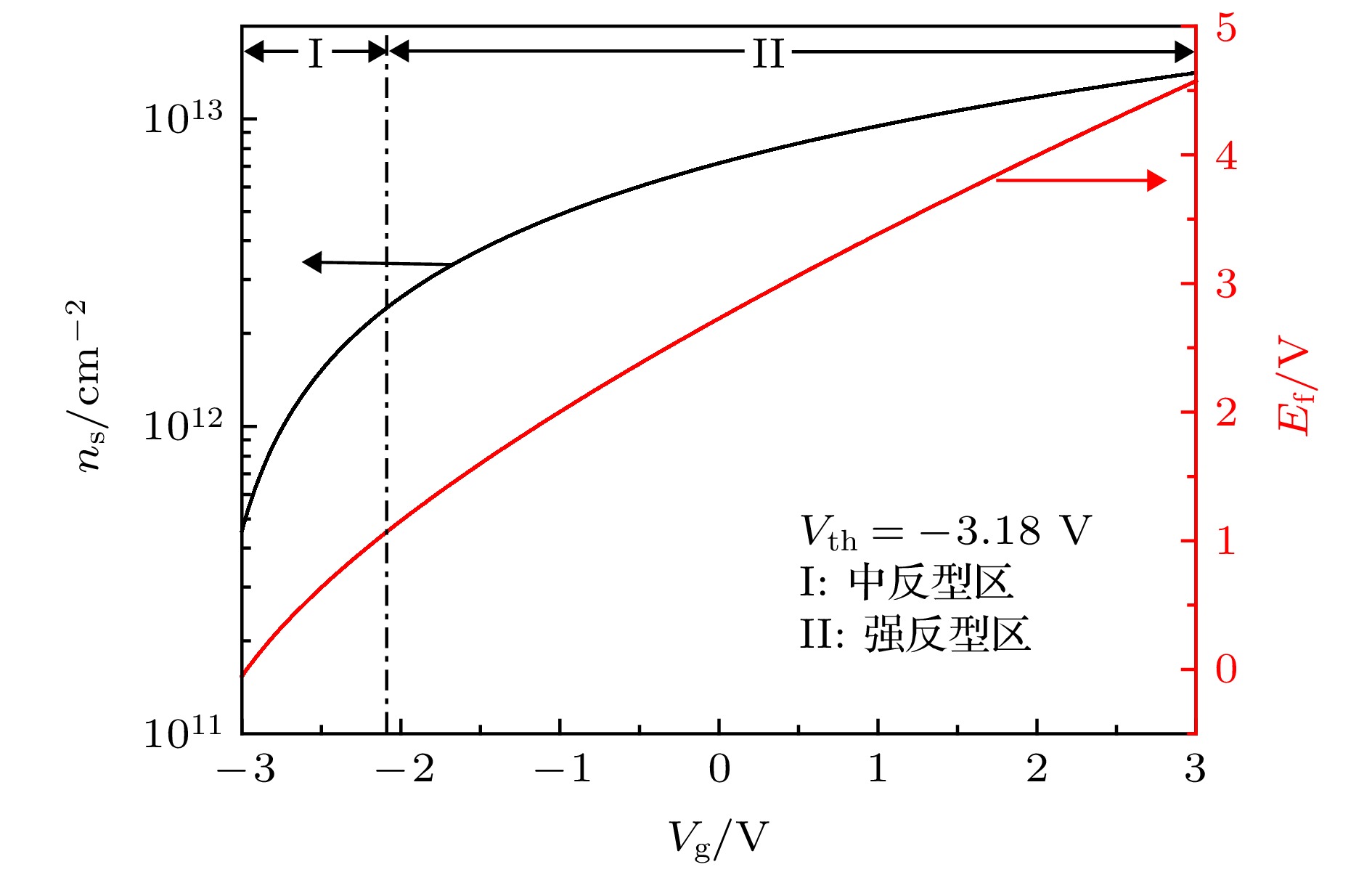 图 6 Vg与2DEG浓度ns和Ef的关系曲线
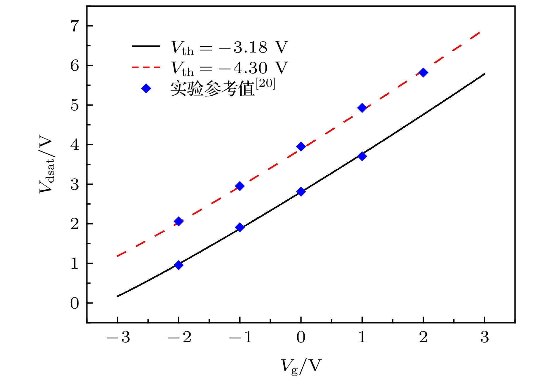 图 7 Vg与Vdsat的关系曲线
 图 8 传统模型和本文模型得到的Vds与Cofd的关系曲线
 图 9 Vth对Cofd的影响关系曲线(插图为Vth与Al组分x和掺杂浓度ND的关系曲线)
 图 10 温度T对Cofd的影响关系曲线
 图 11 不同漏极偏压下Cofd对温度敏感程度的关系曲线