Fund Project:Project supported by the National Natural Science Foundation of China (Grant No. 11804273) and the Key Science and Technology Program of Shaanxi Province, China (Grant No. 2019GY-170).
Received Date:01 July 2021
Accepted Date:26 July 2021
Available Online:17 August 2021
Published Online:05 December 2021
Abstract:The interaction between noble metal nanowires can induce the local surface plasmonic resonance effect, thereby enhancing the distribution of electric field in the nanostructures, which is of very important significance in improving the fluorescence characteristics and enhancing the sensitivity of sensors. In this study, we design several types of tetramers based on precious metals Ag nanostructures, including cylindrical and prismatic Ag tetramers, and by changing the arrangement and the rotation angle of prism nanowires, we simulate the rotation-angle dependent electric field distribution and electric field intensity of X component , and also discuss the physical mechanism of the relationship between the resonant peak position of absorption spectrum and the change of mode volume. The results show that in the Ag nanowires tetramer structure, the electric field in the cylindrical structure is not enhanced obviously, but the electric field in the prismatic structure is greatly enhanced, and an electric dipole resonance mode is produced in the gap between tetramers. The polarization of plasma resonant cavity revels that the morphology plays a decisive role in generating the hot spots, After changing both the combination mode of tetramer nanowires and the rotation angle of the four-prism, the local surface exciton resonance of the unrotated asymmetric tetramer structure is most ideal and has resonance intensity higher than the that of symmetrical four-prism structure. Therefore, our results provide a structural model and theoretical parameters for the enhancement of electric field intensity by local surface plasmon resonance effect. Keywords:Ag nanowire tetramer/ electric dipole resonance/ plasma resonance cavity/ local surface plasmon resonance effect
全文HTML
--> --> --> 1.引 言将金属材料的某一维度限制在纳米尺度, 将获得一种被束缚在结构表面, 且强度剧增的等离子体共振现象, 称为局域表面等离子体共振[1]. 贵金属纳米结构由于具有优异的局域表面等离子体共振特性被广泛研究. 例如, Hong等[2]通过改变Au纳米粒子大小得到了显著的局域表面等离子体共振效应. Xia等[3] 研究了Au纳米阵列的局域表面等离子体与表面等离子体极化子相互作用而产生的场增强效应. Cathcart等[4] 通过构建外壳与重建外壳的方法使纳米粒子同时具备稳定性和精确性. Bingham等[5]研究了Ag纳米粒子的局域表面等离子体散射谱, 实现了粒子扩散与光谱信息的互相耦合. Sherry等[6]用暗场显微镜观察到单个Ag纳米粒子可以呈现出一个全新的等离子体共振效应, 表明了共振会受到纳米粒子尺寸和形状的影响. Xu等[7]研究了五边形单晶Ag纳米线的场增强效应, 结果表明顶点处增强效果最佳. 由此可见, 对于单个贵金属纳米结构, 在产生局域表面等离子体激元的同时, 往往伴随着微结构周围介质环境的场增强效应. 近年来, 为了更好地利用场增强共振效应, 二聚体结构的设计为等离子体效应的研究提供了一个全新的思路[8]. Mahmud等[9]研究发现Au@Ag核壳二聚体结构中呈现出了高频四极和低频偶极局域表面等离子体共振模式. Fernandez-Dom?nguez等[10]探究了二聚体纳米线的光捕获能力, 表明在辐射和非局域效应同时作用于纳米粒子时, 只要选择最佳尺寸的纳米粒子和间隙, 便可最大程度上增强电场强度. Kessentini等[11]将二聚体纳米粒子的间隙制作成倾斜状, 通过改变倾斜的角度可提高二聚体纳米粒子的灵敏度. Khurgin等[12]利用二聚体纳米粒子在间隙内产生场增强现象, 提高了纳米天线对信号的接受强度. 然而, 二聚体结构的共振耦合物理机制仍然存在争议, 研究者们通过不断优化物理模型, 探究等离子共振现象产生的原因. 基于前期的研究背景, 研究者尝试寻找一种更优的结构模型并探讨纳米结构之间的耦合效应[13]. 例如Khoury等[14]对二聚体核壳结构间隙内的空间与光响应进行了理论与模拟分析, 结果表明间隙内的电场增强取决于两个纳米粒子之间的耦合效应. Tserkezis等[15]针对核壳二聚体结构研究了两个核壳纳米粒子之间的强耦合以及非局域等离子体效应. 我们前期也对二聚体核壳结构的电场分布进行了探究[16], 结果表明纳米粒子的相互作用为场强的提高提供了有利条件. 大量的工作中, 虽然研究者们观察到了间隙内的共振增强与极化效应, 但更多的探讨往往集中在极化场下的偶极共振和纳米结构表面场的相互耦合机制, 对于多聚体结构中, 纳米线间隙内产生的等效共振腔很少被报道. 因此, 本文在二聚体结构的基础上构造了几种基于贵金属Ag纳米线的四聚体结构, 金属纳米线的形状由对称度很高的圆柱形和四棱柱形组成, 对比两种结构中的电场分布以及偶极共振与四聚体结构的依赖关系, 并通过改变四聚体的组合方式及四棱柱形纳米线的方位角, 研究多个纳米粒子之间局域表面等离子体效应产生的共振吸收谱对等效共振腔的影响规律, 这在增强荧光特性和提升传感器的灵敏度等方面都有着非常重要的意义. 2.软件与模拟采用Comsol Multiphysics软件的波动光学模块对几种四聚体结构的电场分布进行了模拟研究, 为了方便计算, 将三维纳米线模型(见图1(c)和图1(d))简化为Z方向上无限延长的二维模型(XY面)进行仿真, 在波动光学模块下分别添加边界模式分析和波长域分析, 以得到共振模态下的本征解以及共振吸收谱. 模拟中在二维模型下采用有限元方法进行网格的剖分, 通过边界条件、共振模式设定、模型建立等步骤进行光学响应的研究, 优化纳米结构的尺寸, 主要研究电场强度的X分量与四聚体结构共振位置的依赖关系来对比评估几种四聚体结构的光响应性能, 优化后的圆柱形Ag纳米线直径D为8 nm, 四棱柱形Ag纳米线为圆柱形纳米线的内接六面体, 截面边长为$ 4\sqrt{2} $ nm, 对角线长度L也为8 nm. 另外, 为了同时得到沿纳米线的横向共振模式(L模式)和垂直于纳米线的纵向共振模式(T模式)的吸收谱, 波长域下激励源选择P偏振(电场分量平行入射面: Ex = 1, Ey = 1, Ez = 0)模式, 即L模式和T模式可被同时激发. 图 1 圆柱形(a)与四棱柱(b) Ag四聚体结构中的电场及电场线分布及圆柱形(c)与四棱柱(d)等离子共振腔示意图 Figure1. Electric field and electric field lines distribution in cylinder (a) and quadrangular (b) Ag tetramer nanostructures. Schematic diagram of plasma resonant cavity in cylindrical (c) and (d) tetramer.
3.结果与讨论图1为优化后的圆柱形与四棱柱Ag四聚体纳米线结构中的电场分布, 为了便于观察模态体积的变化, 对图中的电场值范围规范化到–10—10 V/m之间(非电场强度真实值), 根据场强值在XY面内接近或达到10 V/m的面积大小, 确定三维模型下共振模态体积的变化. 由图1(a)可以看出, 四个圆柱形Ag纳米线(C4)的组合使得间隙处的电场有一定程度的增强, 并由电场线分布情况可知, 多聚体结构使得匀强电场产生变化, 在纳米结构内部产生了电偶极子共振[17], 进一步证实了等离子共振耦合效应的出现, 但效果并不明显. 如图1(b)所示, 四个棱柱形Ag纳米线(Q4)的组合使得间隙处的电场急剧增强, 并且在形状较为尖锐的区域都出现了较强的电场分布, 且由电场线分布可以看出, 四棱柱四聚体结构可以在内部形成明显的电偶极子共振效应, 由静电近似[18]可知, 棱柱型纳米线四聚体等离激元共振的极化率远远高于圆柱形纳米线四聚体. 相较于单个纳米线产生的局域表面等离子体, 多聚体结构会在间隙内产生共振耦合效应, 其本征共振模式的强度正比于电场波动方程的振幅, 图2所示为四聚体结构间隙处的电场分布, 棱柱形Ag四聚体共振峰明显强于圆柱形结构, 说明棱柱形四聚体内部的极化强度要远远高于圆柱形. 通过改变四聚体单胞的形貌结构, 可得到急剧的场增强变化, 证实了形貌对于局域表面等离激元共振的形成起到决定性作用, 在纳米结构中的尖点、突起和岛状等结构中, 伴随着“热点”效应[19], 即量子尺寸效应, 这种限制效应会极大增强局域电场, 进而产生共振耦合. 量子尺寸效应可表示为[20] 图 2 圆柱形Ag纳米线四聚体与四棱柱四聚体结构中的电场X分量分布图 Figure2. Distributions of the X-component of the electric field in the cylindrical tetramer and quadrangular tetramer structures of Ag nanowires.
由于热点的产生不仅与尖点和突起等微纳形貌有关, 且与纳米结构的间隙也有密不可分的关系, 通过旋转棱柱形纳米线, 改变尖点的角度, 进而调制圆柱形纳米线与棱柱形尖点之间的耦合距离. 图4所示为C3Q1, C2Q2-Ⅰ, C2Q2-Ⅱ, C1Q3-up, C1Q3-down以及Q4在单个棱柱形纳米线逆时针旋转15°的四聚体结构电场分布图, 由于逆时针和顺时针旋转15°的电场分布几乎一致, 所以图4中仅展示逆时针旋转的情况, 而在考虑对称性的情况下, C1Q3四聚体组合结构中, 会存在两种情况, 即分别旋转对角线上的棱柱纳米线(C1Q3-up)及右下角的纳米线(C1Q3-down). 当棱柱形纳米线经过旋转与圆柱形纳米线之间的间隙变大, 共振耦合效应将会减弱, 尤其在C1Q3-up和C1Q3-down的对比更为明显, 共振腔仅在两者接触部位产生. 图 4 (a) C3Q1, (b) C2Q2-Ⅰ, (c) C2Q2-Ⅱ, (d) C1Q3-up, (e) C1Q3-down 与 (f) Q4单个棱柱形纳米线旋转15°的四聚体结构电场分布图 Figure4. Electric field distributions of (a) C3Q1, (b) C2Q2-Ⅰ, (c) C2Q2-tangent, (d) C1Q3-up, (e) C1Q3-down and (f) Q4 etramer structure after a single prismatic nanowire rotating 15°.
图5所示为仿真区域中心截线, 即未旋转与旋转棱柱形四聚体间隙共振位置(4 nm与–4 nm)处的电场强度分布图. 随着棱柱形纳米线的加入, 调制了共振耦合区域, 改变了等离子体腔的模态体积, 进而影响了共振强度. 纵向平行排列(C2Q2-Ⅰ)的棱柱四聚体相比对角排列(C2Q2-Ⅱ), 仅在极化方向上产生了局域表面等离子体, 共振耦合效应并不明显, 同时, 从C3Q1和C1Q3的对比中可知, 圆柱形与棱柱形产生的热点要明显强于双棱柱形貌结构, 且在C1Q3四聚体结构中, 共振强度最为明显, 强于Q4结构. 图5(b) 中展示的间隙处电场共振强度更加直观的说明单个棱柱形纳米线经过旋转之后对共振腔模式的破坏及调制作用, 不仅对共振位置产生了影响, 同时共振强度减小了大约1/4, 可见形貌对于极化率因子的影响[22], 当纳米结构的接触半径R <5 nm时, 介电常数的极化依赖便不可忽略, 随着极化率提升至无穷大, 等离子激元便发生共振耦合. 图 5 (a)未旋转纳米线四聚体与(b)单个棱柱形纳米线旋转15°的四聚体结构间隙处电场分布图 Figure5. Electric field distributions diagram at the gap between the tetramer (a) without rotation and (b) after 15° rotation of a single prismatic nanowire.

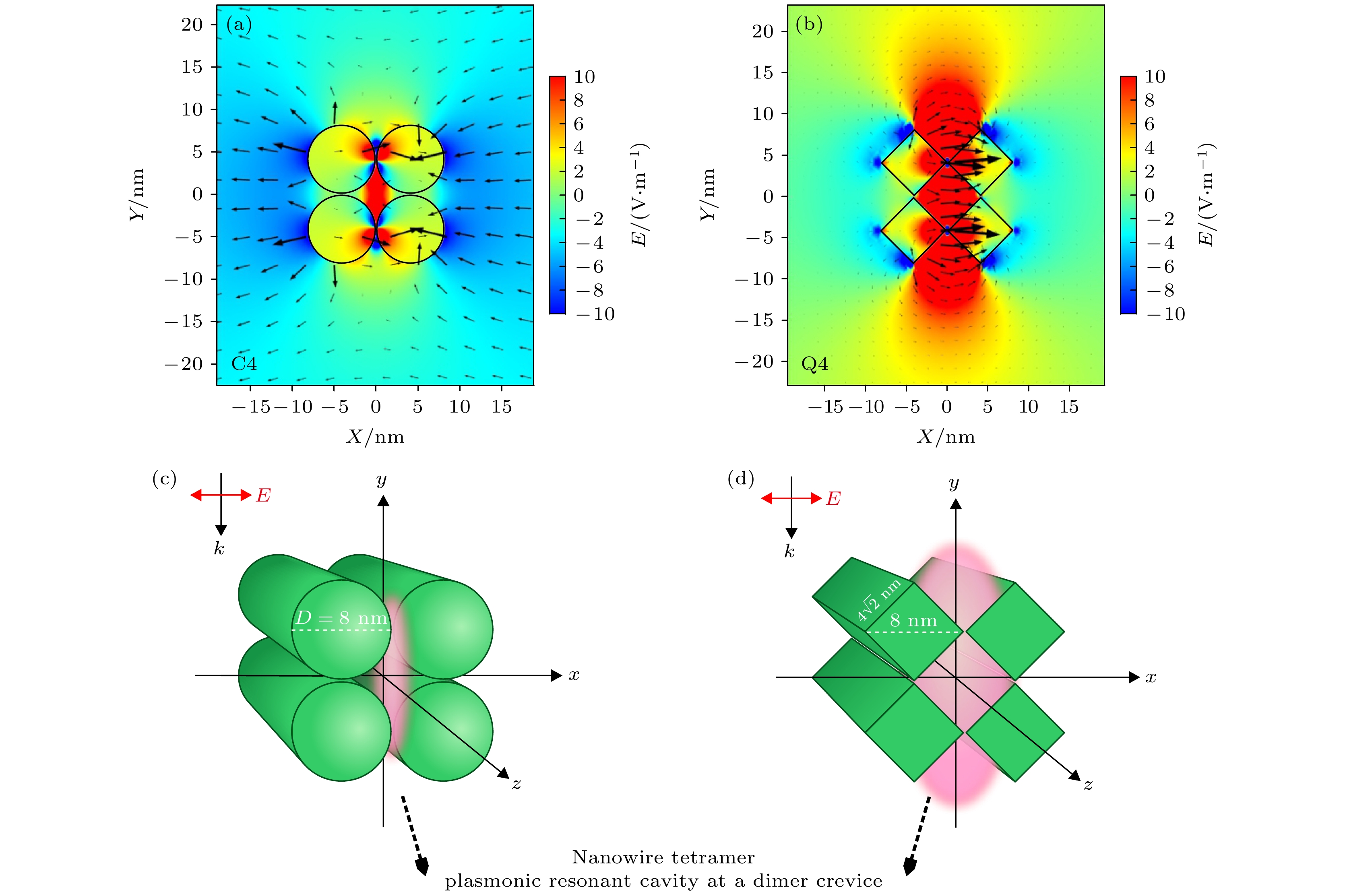 图 1 圆柱形(a)与四棱柱(b) Ag四聚体结构中的电场及电场线分布及圆柱形(c)与四棱柱(d)等离子共振腔示意图
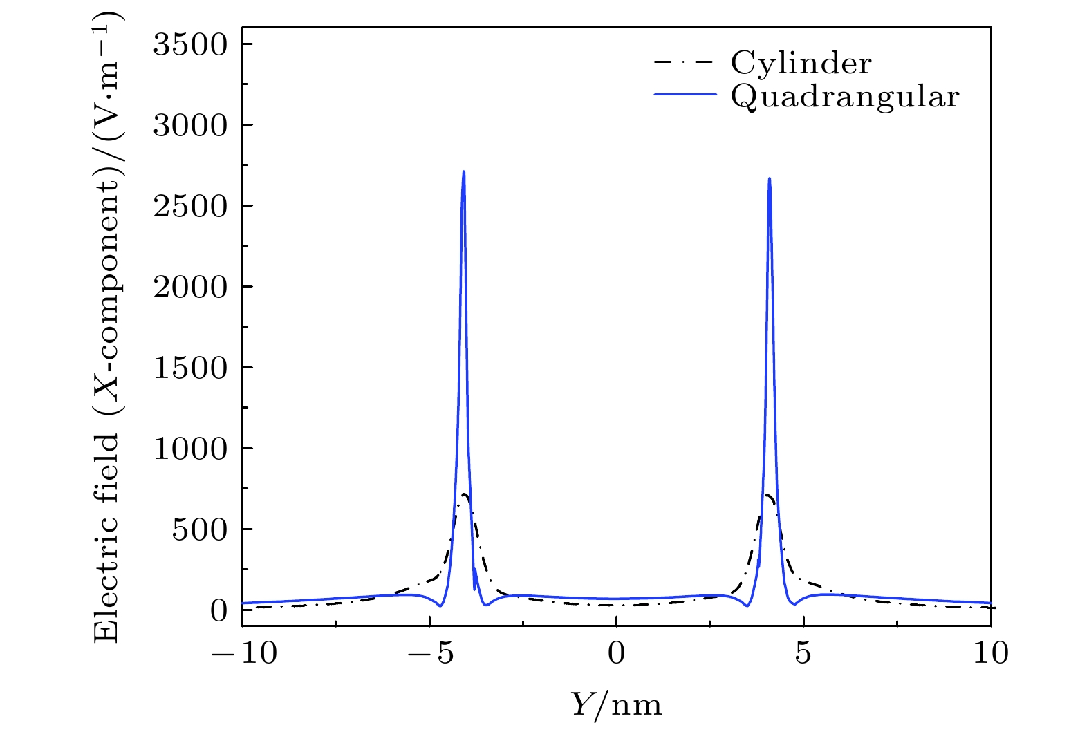 图 2 圆柱形Ag纳米线四聚体与四棱柱四聚体结构中的电场X分量分布图


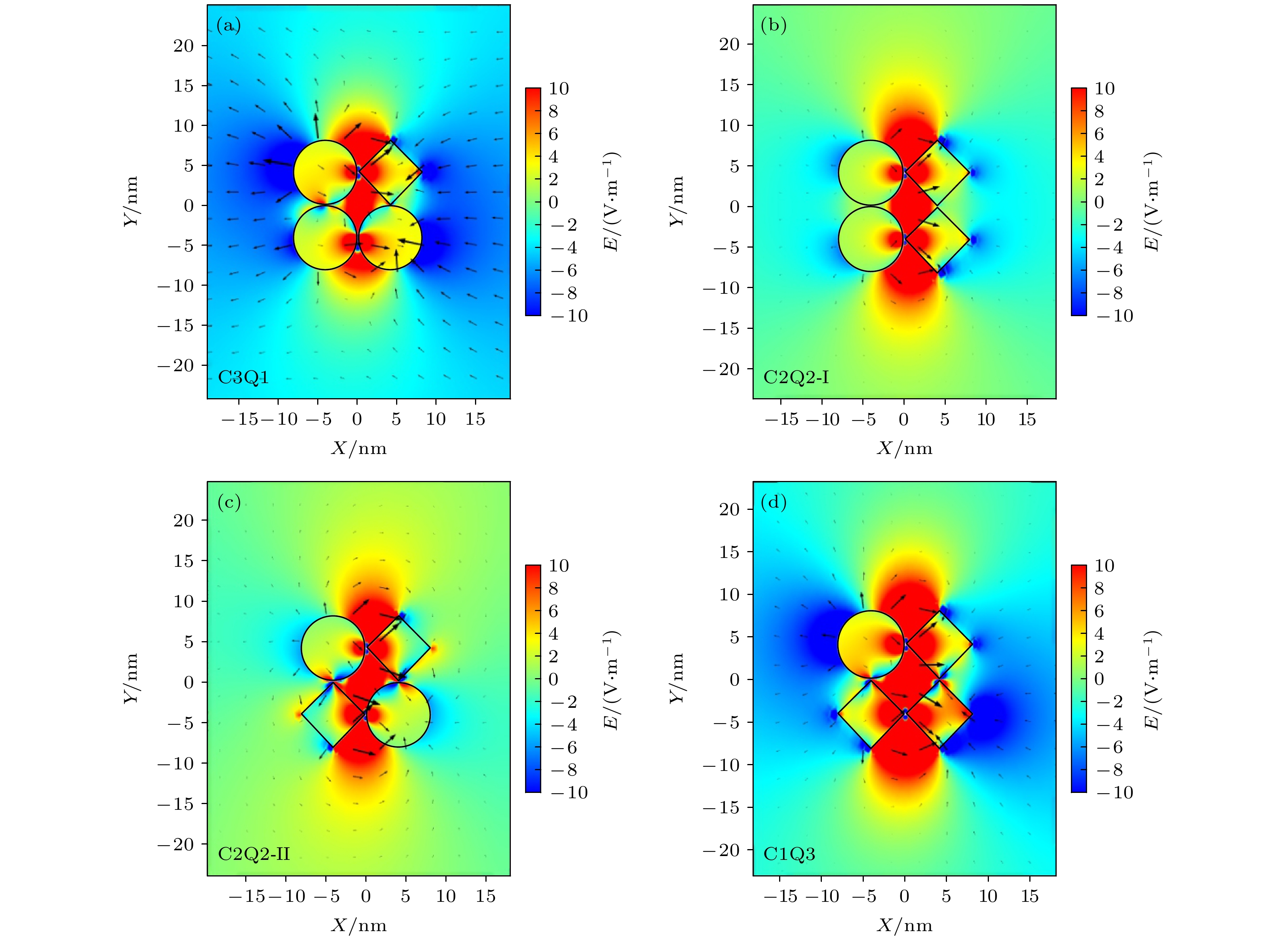 图 3 (a) C3Q1, (b) C2Q2-Ⅰ, (c) C2Q2-Ⅱ 以及 (d) C1Q3Ag纳米线四聚体结构的电场分布
 图 4 (a) C3Q1, (b) C2Q2-Ⅰ, (c) C2Q2-Ⅱ, (d) C1Q3-up, (e) C1Q3-down 与 (f) Q4单个棱柱形纳米线旋转15°的四聚体结构电场分布图
 图 5 (a)未旋转纳米线四聚体与(b)单个棱柱形纳米线旋转15°的四聚体结构间隙处电场分布图
 图 6 不同结构Ag四聚体共振吸收谱 (a) 未旋转圆柱形四聚体与棱柱形四聚体; (b) 未旋转C3Q1, C2Q2-Ⅰ, C2Q2-Ⅱ, C1Q3四聚体; (c) C3Q1, C2Q2-Ⅰ, C2Q2-Ⅱ结构中棱柱纳米线旋转15°四聚体; (d) C1Q3-up, C1Q3-down, Q4结构中棱柱纳米线旋转15°四聚体

