全文HTML
--> --> -->目前, 传统的光学传感器体积大, 不易携带, 为使传感器小型化, 研究者提出了许多可微型化的传感结构. 由于HPWs与周围环境的强相互作用和局域增强效应, HPWs为实现新型生物化学传感提供了一种可行的方案.
多孔硅(porous silicon, PS)具有良好的光学特性, 例如光致发光效应和反射干涉效应. 由于PS有较大的比表面积, 增强了光与物质的相互作用. 另外, PS的可调孔隙率随制造参数的变化而变化[21], 使其折射率(refractive index, RI)在空气和多孔硅之间可调. 由于PS的这些优势, 它被广泛应用于光电子学领域[22–26]、电力工程[27]和传感领域[28]. 此外, 由于氟化钙穿透性好, 宽带透过率高、环境抗性强和独特光学特性, 致使它在半导体的应用上有着悠久的传统. 并且氟化钙(CaF2)红外透过率高、光谱色散低和更宽的中红外(mid-infrared, MIR)光谱透明窗口, 是一种很有前途的SiO2替代材料.
本文研究了一种非对称银膜PS-CaF2混合等离子体波导(PS-CaF2 HPW), 它是在氮化硅波导的顶面和一侧侧壁沉积覆盖氟化钙层和银薄膜层而形成的一种非对称波导结构. 利用有限元方法(finite element method, FEM)对波导中的等离子体模式进行了数值计算, 研究了波导中存在的两个基模在中红外波长(3.5 μm)处的有效折射率、品质因数、有效模场面积和传输损耗特性, 并采用参数扫描方法对结构的几何尺寸参数进行了优化. 通过改变波导包层的折射率, 研究了利用等离子体模式进行传感时的波导灵敏度. 随后, 分析了非对称银膜PS-CaF2混合等离子体波导的制造容差.
 图 1 非对称银膜的PS-CaF2混合等离子体波导示意图 (a)三维图; (b)波导截面图
Figure1. Schematic diagram of Ag film coated asymmetric PS-CaF2 hybrid plasma waveguide: (a) 3D diagram; (b) cross-sectional view.
为了衡量非对称银膜PS-CaF2 混合等离子体波导的模式特性、传输特性和传感性能, 通常用有效折射率(neff)、品质因数(FOM)、传输损耗(α)、归一化模场面积(A)以及波导灵敏度(Swg)参数来进行分析.
品质因数(FOM)可综合衡量波导的模式特性, 计算公式如下:
模式的有效折射率虚部与其传输损耗(α)成正比:
传感性能通常用灵敏度(sensitivity, S)表示, 它描述了待测物质的变化与某种物理量的变化的对应关系. 灵敏度一般分为两部分: 器件灵敏度(device sensitivity, Sdev)和波导灵敏度(waveguide sensitivity, Swg). 器件灵敏度取决于器件的性能, 而波导灵敏度取决于波导结构, 因此, 本文对非对称银膜PS-CaF2 混合等离子体波导的波导灵敏度进行了分析, 其定义为 [31]
本文采用FEM对非对称银膜PS-CaF2混合等离子体波导在中红外波段的模式特性、传输特性和波导灵敏度进行了研究. 根据光场的模式分析原理, 将非对称银膜PS-CaF2混合等离子体波导的待计算区域剖分为非均匀三角形网格, CaF2和Ag层的最小网格值为5 nm, 其他计算区域为0.3 μm, 在边界上使用散射边界条件来模拟吸收边界, 并通过收敛性测试确保计算的准确性.
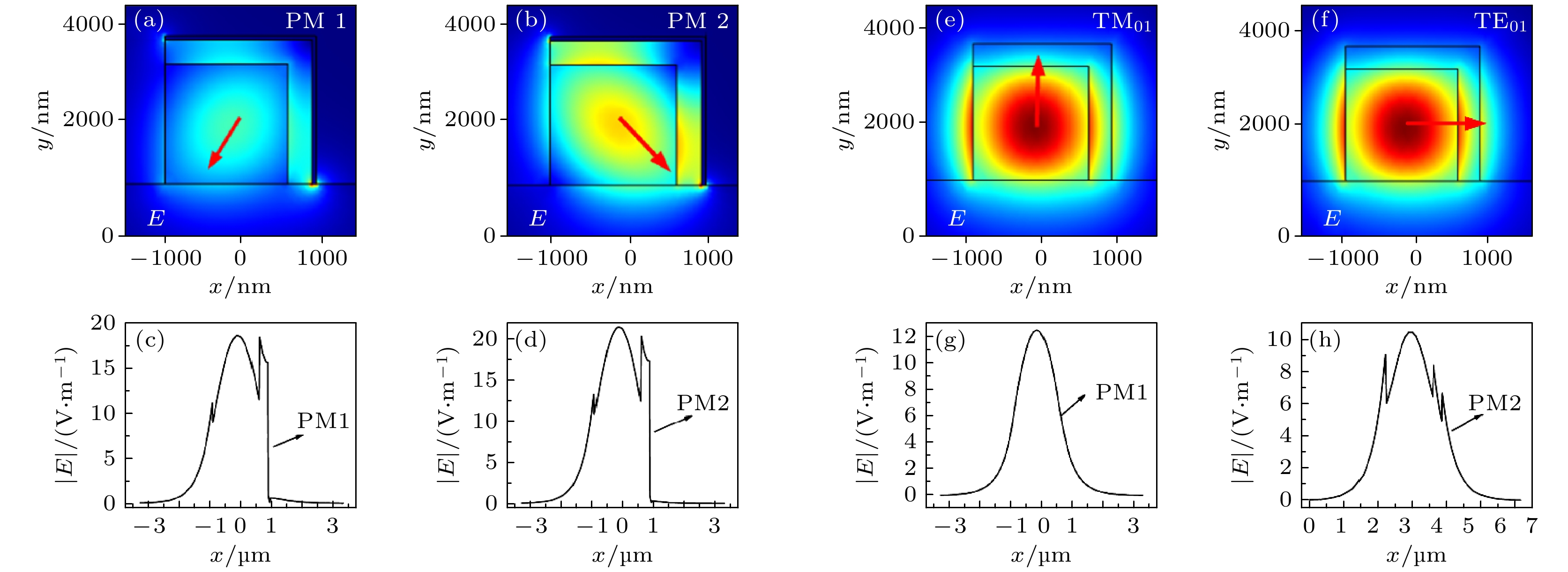 图 2 W1 (= H1) = 1500 nm, W2 (= H2) = 300 nm和W3 (= H3) = 70时, 非对称银膜PS-CaF2混合等离子体波导中不同模式的模场分布图 (a) PM 1; (b) PM 2; 波导中心沿x方向的电场分布图 (c) PM 1; (d) PM 2; W1 (= H1) = 1500 nm和W2 (= H2) = 300 nm时, 无银膜普通波导的模场分布图 (e) TM01; (f) TE01; 波导中心沿x方向的电场分布图 (g) TM01, (h) TE01
Figure2. Mode field distributions of (a) PM 1 and (b) PM 2; electric field distribution along the x axis of (c) PM 1 and (d) PM 2; mode field distributions of (e) TM01 and (f) TE01; electric field distribution along the x axis of (g) TM01 and (h) TE01 when W1 (= H1) = 1500 nm, W2 (= H2) = 300 nm and W3 (= H3) = 70.
为了分析非对称银膜对模式偏振方向的影响, 仿真了无Ag膜的普通波导, 其两个基模如图2(g)和图2(f)所示, 图中红色箭头表示电场方向. 对比图2(a)、图2(b)和图2(e)、图2(f)可以看出, 相比无Ag膜的波导, PM 1和PM 2的电场方向偏转了45°角. 对比图2(c)、图2(d)和图2(g)、图2(h)可知, 增加Ag膜的等离子体波导的PS芯层的模式能量比普通波导高.
图3(a)—(c)是PM 1和PM 2的Re和α随W1, W2和W3 的变化曲线图4(a)—(c)是PM 1和PM 2的FOM和A随W1, W2和W3 的变化曲线. 从图4(a)可以看出, 当W2 = 300 nm, W3 = 70 nm时, 随着W1增大, FOM和A都增加. 这是因为W1增大, 更多的模场能量被限制在了PS层, 减小了模式的有效模场面积和损耗(折射率虚部), 从而使FOM和A增大. 如图4(b)所示, 当W1 = 1500 nm, W3 = 70 nm时, 在W2 = 350 nm之前, PM 2的A逐渐减小而PM 1的A则是逐渐增大, 而在W2 = 350 nm之后PM 1和PM 2的A几乎都保持不变. PM 1的FOM在整个过程中是一直增大, 而在W2 = 350 nm之前, PM 2的FOM先减小, 之后缓慢增大. 在图4(c)中, 当W1 = 1500 nm, W2 = 300 nm时, 在W3 = 70 nm之前, PM 1和PM 2的FOM随着增加, 而在W3 = 70 nm之后, 则都几乎保持不变, 这与银膜厚度满足模式指数衰减要求相关. PM 2的A保持一直不变的状态; 在W3 = 150 nm之前, PM 1的A呈现增长趋势, 之后基本保持不变.
 图 3 PM 1和PM 2的Re(neff)和α随(a)W1 (= H1), (b) W2 (= H2) 和 (c) W3 (= H3)变化的规律, W1 (= H1), W2 (= H2) 和W3 (= H3)分别取1500 nm, 300 nm和70 nm
Figure3. Re(neff) and α of the PM 1 and PM 2 with different: (a) W1 (= H1) at W2 (= H2) = 300 nm and W3 (= H3) = 70 nm; (b) W2 (= H2) at W1 (= H1) = 1500 nm and W3 (= H3) = 70 nm; (c) W3 (= H3) at W2 (= H2) = 300 nm and W1 (= H1) = 1500 nm.
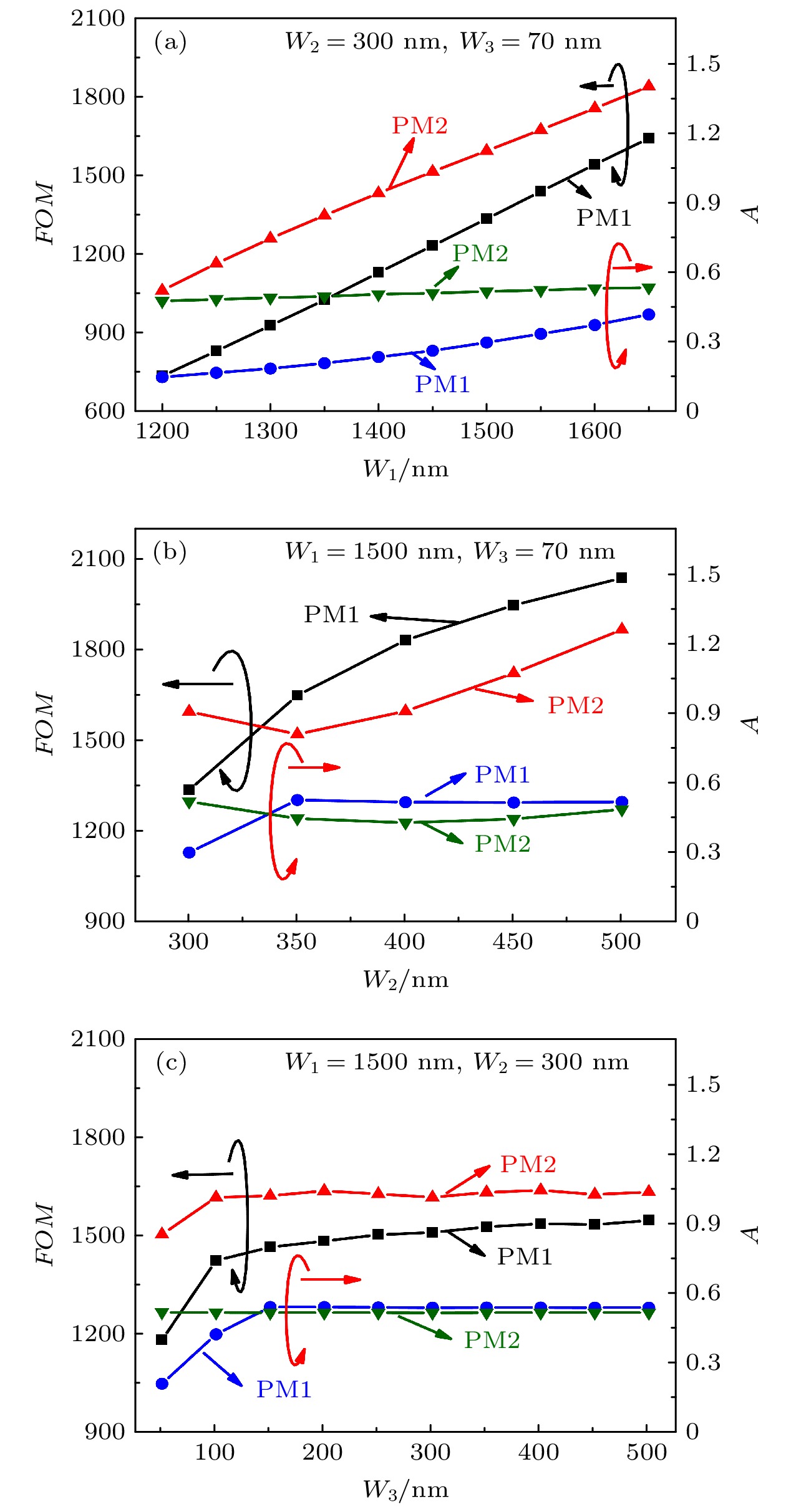 图 4 PM 1和PM 2 的FOM 和A随(a)W1 (= H1), (b) W2 (= H2)和(c) W3 (= H3)变化的规律, W1 (= H1), W2 (= H2) 和W3 (= H3)分别取1500 nm, 300 nm和70 nm
Figure4. FOM and A of the PM 1 and PM 2 with different: (a) W1 (= H1) at W2 (= H2) = 300 nm and W3 (= H3) = 70 nm; (b) W2(= H2) at W1 (= H1) = 1500 nm and W3 (= H3) = 70 nm; (c) W3 (= H3) at W2 (= H2) = 300 nm and W1 (= H1) = 1500 nm.
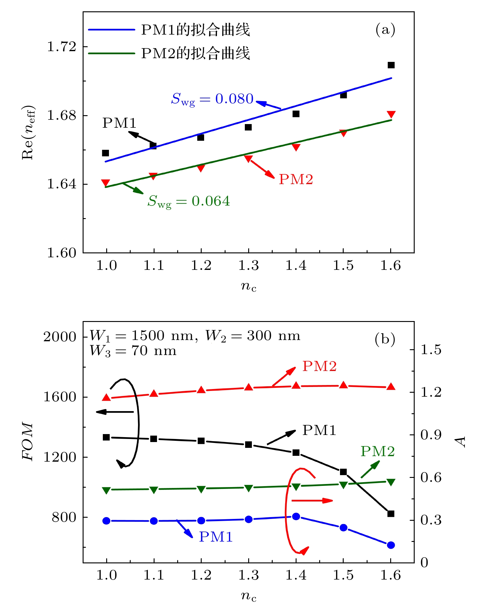 图 5 在不同的nc下, PM 1和PM 2的(a) Re(neff), (b) FOM和A的变化规律, W1 (= H1), W2 (= H2) 和W3 (= H3)分别取1500 nm, 300 nm和70 nm
Figure5. (a) Re(neff) and (b) FOM and A of the PM 1 and PM 2 with different nc as W1 (= H1) = 1500 nm, W2 (= H2) = 300 nm and W3 (= H3) = 70 nm.
图6(a)—(c)是非对称Ag膜多孔硅-氟化钙混合等离子体波导的Swg随着W1, W2和W3的变化情况. 从图6(a)中可以看出, 当W2 = 300 nm和W3 = 70 nm时, PM 1和PM 2的Swg随W1的增加而减小. 由于W1的增加有利于更多的模式能量被限制在PS芯层, 从而导致PM 1和PM 2的Swg减小. 如图6(b)所示, 当W1 = 1500 nm和W3 = 70 nm时, PM 1的Swg 随着W2的增加而减小, 然而PM 2的Swg反而增大. 这是因为模式的极化方向不同, 致使PM 1和PM 2的Swg呈现出相反的变化趋势. 图6(c)中, 当W1 = 1500 nm和W2 = 300 nm时, PM 1和PM 2的Swg 随着W3变化而保持不变, 说明W3的变化基本不影响Swg. 因为模式的模场能量几乎都被限制在PS层和CaF2层中(如图2(a)和图2(b)所示). 当W1 = 1500 nm, W2 = 300 nm和W3 = 70 nm时, PM 1和PM 2的波导灵敏度分别为0.080和0.065.
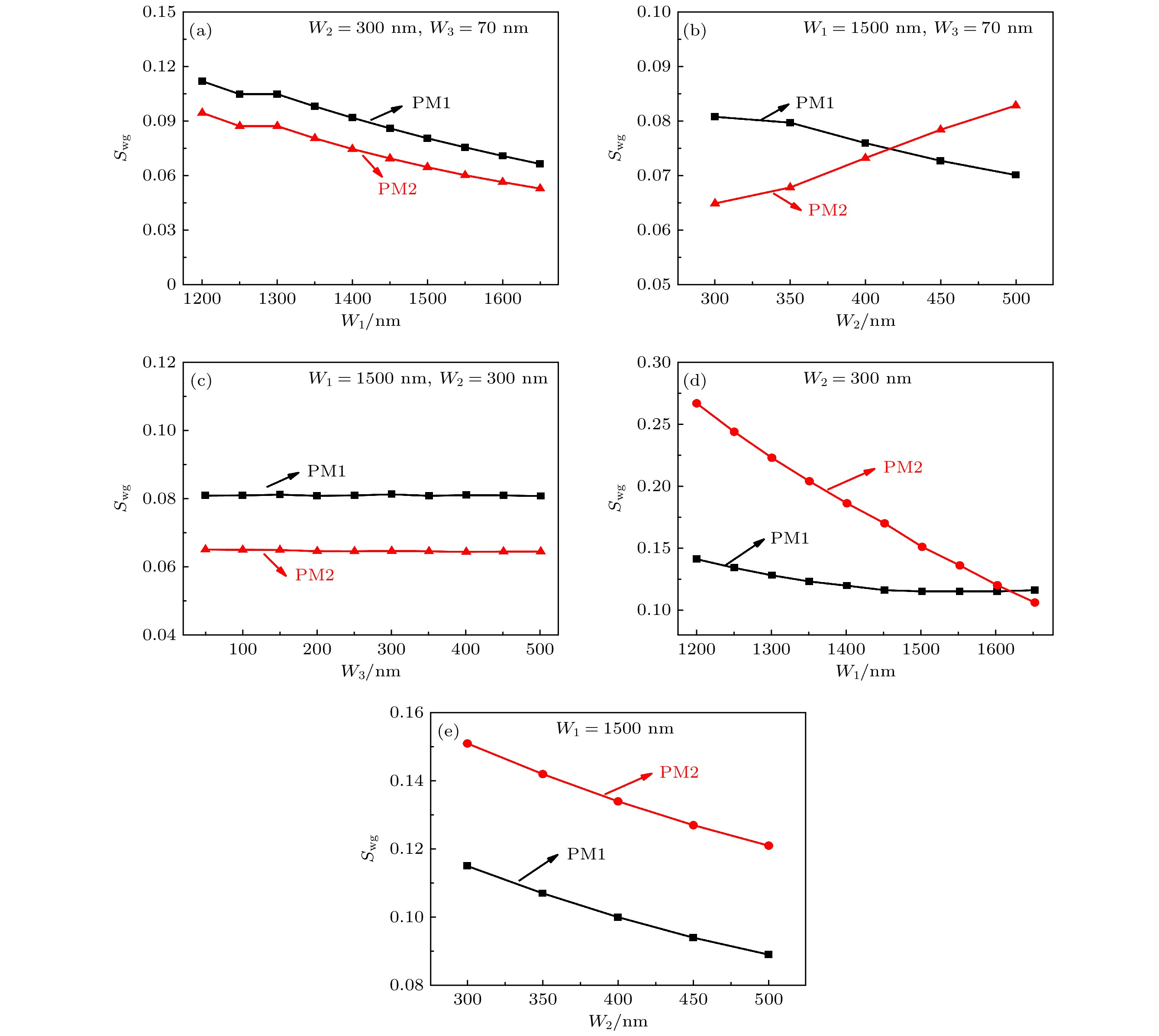 图 6 非对称PS-CaF2混合等离子体波导的PM 1 和 PM 2 的Swg 随(a) W1 (= H1), (b) W2 (= H2)和(c) W3 (= H3) 的变化规律, W1 (= H1), W2 (= H2) 和W3 (= H3)分别取1500 nm, 300 nm和70 nm; 无Ag膜波导的PM 1 和 PM 2 的Swg 随(d) W1 (= H1)和 (e) W2 (= H2)的变化规律, W1(= H1)和W2(= H2)分别取1500 nm和300 nm
Figure6. with an asymmetric Ag film of Swg of the PM 1 and PM 2 in the PS-CaF2HPW with an asymmetric Ag films with different: (a) W1 (= H1) at W2 (= H2) = 300 nm and W3 (= H3) = 70 nm; (b) W2 (= H2) at W1 (= H1) = 1500 nm and W3 (= H3) = 70 nm; (c) W3 (= H3) at W2 (= H2) = 300 nm and W1 (= H1) = 1500 nm. Without an asymmetric Ag film of Swg of the PM 1 and PM 2 in the waveguide without an asymmetric Ag film of with different (d) W1 (= H1) at W2 (= H2) = 300 nm; (b) W2 (= H2) at W1 (= H1) = 1500 nm.
为了分析Ag膜对波导灵敏度的影响, 无Ag膜时Swg随着W1和W2的变化情况如图6(d)和图6(e)所示. 从图6(d)中可以看出, 当W2 = 300 nm时, PM 1和PM 2的Swg随W1的增加而减小, 但PM 1的减小幅度远小于PM 2. 因为随着W1的增大, 对于PM 2来说, 模场能量被更多地限制在PS层, 而PM 1的模场能量分布主要集中在在PS层中心位置, 故W1的增大对PM 1的影响并不大. 如图6(f)所示, 当W1 = 1500 nm时, PM 1和PM 2的Swg随着W2的增大而逐渐变小. 因为随着W2的增大, 被限制在PS层和CaF2层模场能量增加. 当W1 = 1500 nm和W2 = 300 nm时, PM 1和PM 2的灵敏度分别为0.115和0.151. 增加非对称Ag膜后, 波导的表面等离子体效应降低了结构的波导灵敏度, 然而, 能量分布更加集中的优势可以提高传感系统的集成度, 有利于提高传感的器件灵敏度. 这里提出的非对称Ag膜结构还可以实现不同偏振模式的复用和多参数传感.
温度变化对波导灵敏度的影响是传感结构必须考虑的因素, 因此, 我们分析了温度变化对波导灵敏度的影响, 如图7(a)所示. 在环境温度为295 K附近时, PS, CaF2, PMMA和Ag的热光系数(thermo-optical coefficient, TOC)分别是2.45 × 10⁻⁵/K, 2.8 × 10⁻⁵/K, –1.1 × 10⁻⁴/K和2.13 × 10–4/K. 当温度变化时, 波导的Swg基本不变化. 由图7(b)和图7(c)可知, 温度变化对α, FOM和A的影响也不大, 几乎不发生变化. 从图7可以看出, 波导的性能受温度影响较小.
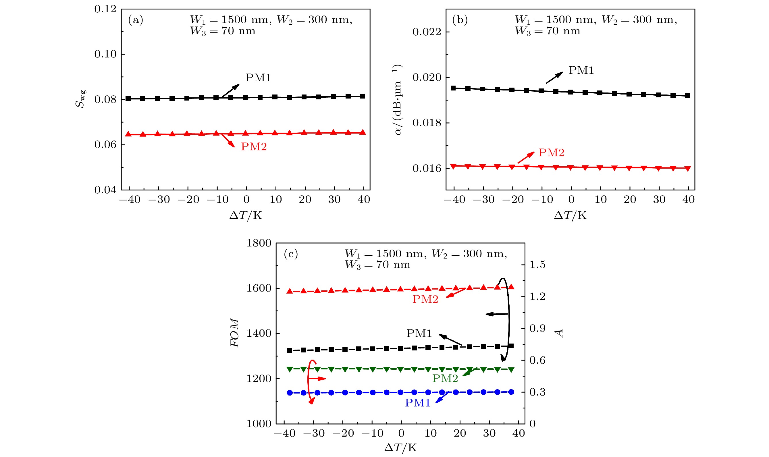 图 7 W1 (= H1) = 1500 nm, W2 (= H2) = 300 nm和W3 (= H3) = 70 nm时, 在不同的ΔT下 (a) Re(neff), (b) α, (c) FOM和A的变化规律
Figure7. (a) Re(neff), (b) α, (c) FOM and A with different ΔT as W1 (= H1) = 1500 nm, W2 (= H2) = 300 nm and W3 (= H3) = 70 nm
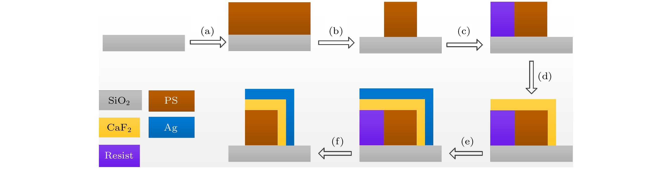 图 8 制造流程 (a)在SiO2衬底上外延生长PS层; (b)电子束光刻使其成型; (c)涂上抗蚀剂; (d) 在PS上外延生长CaF2层; (e) 倾斜沉积金属Ag层; (f)电子束光刻使其成型, 并清除抗蚀剂
Figure8. (a) Grow PS on a SiO2 substrate; (b) pattern the resist through E-beam lithography; (c) it is coated with a resist; (d) grow CaF2 layers epitaxially on a PS layer; (e) oblique deposition of metal Ag; (f) electron beam lithography moulds it and removes the resist.
尺寸容差对非对称银膜PS-CaF2 混合等离子体波导的影响是波导实际应用必须考虑的问题, 因此需要讨论尺寸容差对非对称银膜PS-CaF2 混合等离子体波导性能的影响. 本文设计的非对称银膜PS-CaF2 混合等离子体波导部分覆盖CaF2和Ag薄膜, 在制造过程中要求较大的对准容差. 尺寸容差对非对称银膜PS-CaF2 混合等离子体波导性能的影响如图9—图11所示. 根据前文的参数优化, 在下面的仿真过程中, W1(= H1), W2(= H2)和W3(= H3)分别为1500 nm, 300 nm和70 nm. 此时, PM 1和PM 2的FOM分别是1335.45和1594.99; A分别为0.30, 0.52; Swg分别为0.080, 0.064. 在 ± 10 nm的容差范围内, 研究了ΔW1, ΔH1, ΔW2, ΔH2, ΔW3和ΔH3对FOM, A和Swg的影响.
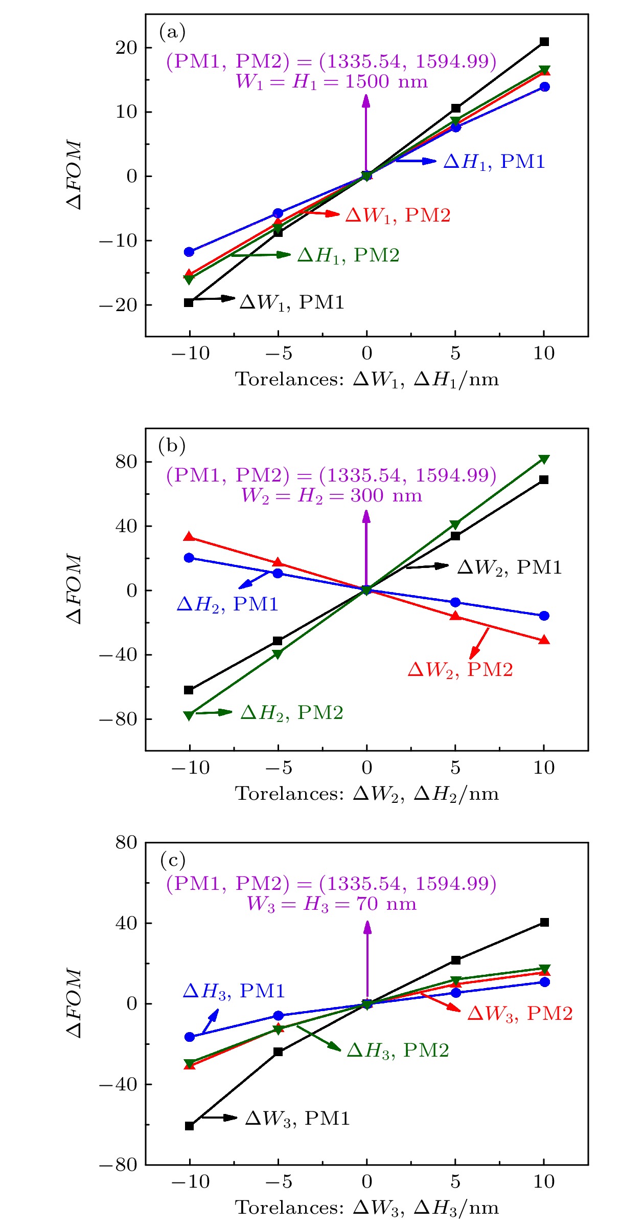 图 9 不同的尺寸容差下, PM 1和PM 2 的FOM的变化 (ΔFOM)随(a) ΔW1和ΔH, (b) ΔW2和ΔH2; (c) ΔW3和ΔH3的变化规律, W1 (= H1), W2 (= H2) 和W3 (= H3)分别取1500 nm, 300 nm和70 nm
Figure9. The changes of FOM (ΔFOM
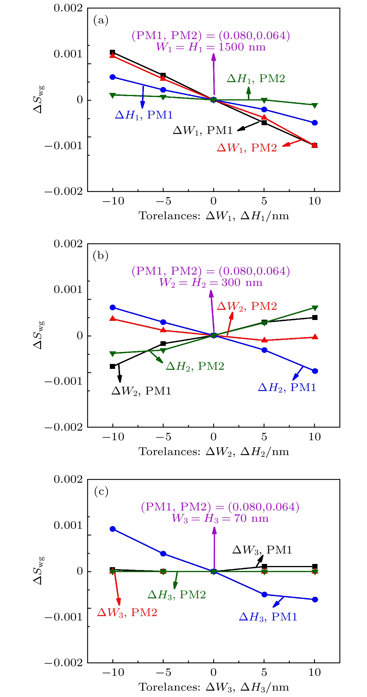 图 11 不同的尺寸容差, PM 1和PM 2 的Swg (ΔSwg)随(a) ΔW1和ΔH1, (b) ΔW2和ΔH2, (c) ΔW3和ΔH3的变化规律. W1(= H1), W2(= H2) 和W3(= H3)分别取1500 nm, 300 nm和70 nm
Figure11. The changes of Swg (ΔSwg) for the PM 1 and PM 2 with different dimensional tolerances: (a) ΔW1 and ΔH1 at W2(= H2) = 300 nm and W3(= H3) = 70 nm; (b) ΔW2 and ΔH2 at W1(= H1) = 1500 nm and W3(= H3) = 70 nm; (c) ΔW3 and ΔH3 at W1(= H1) = 1500 nm and W2(= H2) = 300 nm.
不同尺寸容差下, FOM的变化(ΔFOM)如图9(a)—(c)所示. 在图9(a)中, ΔW1和ΔH1的变化对ΔFOM的影响较小, 变化幅度小于20.7和16.5. 然而, 因为银膜厚度与欧姆损耗紧密相关, ΔW3和ΔH3的变化对ΔFOM有明显的影响. 对于PM 1来说, ΔW1(ΔW2或ΔW3)的影响比ΔH1(ΔH2或ΔH3)大. 对于PM 2来说, ΔW1(或ΔW3)和ΔH1(或ΔH3)对ΔFOM的影响基本一样. 由于极化方向的不同, ΔW2(或ΔH2)对PM 1和PM 2的ΔFOM有相反的影响, 如图9(b)所示. 由图9可知, 不同尺寸容差对FOM的影响小于80.
不同尺寸容差下, A的变化(ΔA)如图10(a)—(c)所示. 在图10(a)中, ΔW1(或ΔH1)对于PM 2的A几乎没有影响; 而对于PM 1来说, A都随ΔW1(或ΔH1)增大而增加, 但ΔW1的影响更明显. 在图10(b)中, ΔW2(或ΔH2)对PM 2的A没有明显影响; 而对ΔW2和ΔH2对PM 1的A的影响呈现相反的趋势. 如图10(c)所示, ΔW3 (或ΔH3)对PM 2的A几乎没有影响; 然而ΔW3和ΔH3对PM 1的A有不同的影响, A先随ΔW3增大而增大然后几乎不变, ΔH3对A几乎没影响. 总的来说, 不同尺寸容差对A的影响都小于0.06.
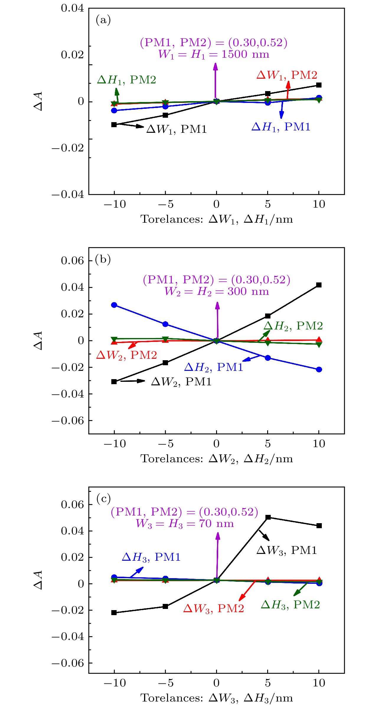 图 10 在不同的尺寸容差下, PM 1和PM 2 的A 的变化(ΔA)随(a) ΔW1和ΔH1, (b) ΔW2和ΔH2, (c) ΔW3和ΔH3的变化规律. W1(= H1), W2(= H2) 和W3(= H3)分别取1500 nm, 300 nm和70 nm
Figure10. The changes of A (ΔA) for the PM 1 and PM 2 with different dimensional tolerances: (a) ΔW1 and ΔH1 at W2 (= H2) = 300 nm and W3 (= H3) = 70 nm; (b) ΔW2 and ΔH2 at W1 (= H1) = 1500 nm and W3 (= H3) = 70 nm; and (c) ΔW3 and ΔH3 at W1 (= H1) = 1500 nm and W2 (= H2) = 300 nm.
不同尺寸容差, Swg的变化(ΔSwg)如图11(a)—(c)所示. 在图11(a)中, ΔW1(或ΔH1)对PM 1和PM 2的Swg的影响趋势基本相同. PM 1和PM 2 的Swg随着ΔW1增大逐渐减小. ΔH1对PM 1和PM 2 的Swg的影响比ΔW1小. 从图11(b)可知, 对于PM 1和PM 2, ΔW2对Swg的影响与ΔH2相反. 也就是说, 随ΔW2的增大, PM 1的Swg逐渐增大而PM 2的Swg逐渐减小. 然而随着ΔH2的增大, PM 2的Swg逐渐增大而PM 1的Swg却逐渐减小. 从图11(c)上可以看出, ΔW3对PM 1和PM 2的Swg都几乎没有影响; ΔH3对PM 2的Swg也没有明显影响, 而只对PM 1的Swg有影响. 由以上可知, 不同尺寸容差对Swg的影响都小于0.001.
