Fund Project:Project supported by the National Natural Science Foundation of China (Grant No. 61734002)
Received Date:16 March 2021
Accepted Date:04 May 2021
Available Online:07 June 2021
Published Online:20 September 2021
Abstract:The spin-wave coupling device is used as a connection unit to solve the connection problem between spin-wave devices. However, the current size is too large in comparison with the nano-scale process, which is caused by the low efficiency of the spin wave within it. Therefore, we propose the spin-wave directional coupler based on Y3Fe5O12-CoFeB coupling which can improve the current dilemma to a certain extent. By filling the gap layer of two spin-wave waveguides (Y3Fe5O12) placed in parallel with CoFeB material, it is found that the dispersion relationship of the spin wave changes in the data calculation of the micromagnetic simulation software Mumax3. The existence of CoFeB makes the transmission efficiency of the spin wave between the two waveguides higher than in the case without any filling, the enhancement effect is about 4 times where coupling length is reduced from the original 2000 nm to 500 nm, which is conducive to the miniaturization and integration of the spin-wave directional coupler design. From the perspective of the entire device, further analysis indicates that owing to the high saturation magnetization of CoFeB (approximately 8 times that of Y3Fe5O12), the effective field in the Y3Fe5O12-CoFeB directional coupler is greatly enhanced, which leads the spin wave dispersion curve in the waveguide to change. At the same time, the energy of the entire system also increases several times, which is mainly caused by the increase of dipole energy and exchange energy. Then a greater contribution of dipole energy is obtained by changing the size of the device. After that, we study the relationship between the coupling length and the device size and the external magnetic field, then draw a general rule which can play a role in designing any directional couplers with similar structures. Finally, our view points are given from the different spin wave excitation frequencies, gap layer filling materials, internal roughness of the directional coupler, and spin wave lifetime by considering the problems that may occur in practical applications with the Y3Fe5O12-CoFeB directional coupler. In conclusion, our proposed Y3Fe5O12-CoFeB directional coupler structure can effectively enhance the coupling efficiency, and it can also provide a new idea for the application of the interaction between composite materials. Keywords:spin wave/ directional coupler/ micromagnetic simulation/ coupling length
微波场的方向为y方向, 幅值h0 = 0.001 mT, 截止频率fc = 20 GHz, t0 = 50 ps. 图2(a)为该sinc场在频域下的曲线图, 在sinc场的作用下可以产生0—10 GHz的等幅磁场, 可以作为色散曲线的激励场. 通过计算得到YIG单波导的色散关系如图2(b)所示, 这是该种结构下的最低宽度模式的自旋波的色散曲线. 图 2 (a) 色散曲线求解中激励场在频域下的显示; (b) 孤立YIG波导中的色散曲线 Figure2. (a) Display of the excitation field in the frequency domain in the solution of the dispersion curve; (b) dispersion curve of isolated YIG waveguide.
之后仿真模拟并计算了间隙为Air (YIG/Air/YIG结构)和CoFeB (YIG/CoFeB/YIG结构)的双YIG波导的色散曲线, 如图3所示, 可以发现色散曲线发生了劈裂, 由原先的最低宽度模式分裂为两种集体模式: 对称模式和反对称模式(对应S和AS, 参见图3(a)), 从而使得两种自旋波模式在每个单个波导中同时被激发, 在同一频率的激励下具有不同的波数, 因此自旋波能量在两个波导之间周期性地传输和分配. 图3和图3(b)分别表示在间隙层中填充有空气和CoFeB的定向耦合器中的自旋波色散关系, 可以很清楚地看到在CoFeB填充结构下S态和AS态的间隔要大得多. 在2.5—5 GHz下的自旋波可以有效地进行传播, 为了便于观察出两种结构下自旋波耦合长度的变化, 在2.88 GHz的频点上激励自旋波(图3(a)和图3(b)中红线处的$ \Delta {k_1} $和$ \Delta {k_2} $代表两种情况下的波数差), 可以清楚地看到后者比前者大, 约为前者的4倍. 图 3 间隙处分别填充(a) Air和(b) CoFeB情况下的自旋波色散图 Figure3. Spin wave dispersion curve when the gap is filled with (a) Air and (b) CoFeB.
将自旋波的能量从一个波导完全传播到另一个波导所需的距离定义为耦合长度, 其值如下:
$ L = {\text{π}}/\left| {{k_{\text{s}}} - {k_{{\text{as}}}}} \right|, $
其中, $ {P_1} $为波导S1中左侧的输入能量, $ L(y) $是指耦合的波导之间相互作用的长度. 从图4(a)可以看出, 在填充CoFeB的耦合结构中, 能量完全转换要大约500 nm的距离, 而这个值在填充空气的结构中是2000 nm左右. 此外, 为了更直观地说明这一情况, 通过微带天线激励了2.88 GHz下的自旋波(图4(b)). 红色和蓝色像素代表自旋波的幅度, 颜色越深, 幅度就越强, 这反映了两种结构下能量的耦合过程. 其中的L1和L2分别表示间隙为Air以及CoFeB的定向耦合器下的耦合长度, 可以很直观地观察到, $ {L_1} \approx 4{L_2}$. 因此, 耦合长度对于自旋波器件的设计来说是一个关键参数, 它影响着整个器件的大小以及最高使用频率限制. 图 4 (a) 定向耦合器的输出随着波导长度变化的关系图; (b) 2.88 GHz下间隙处填充Air和CoFeB的定向耦合器工作过程中自旋波传播彩图 Figure4. (a) Relationship between the output of the directional coupler and the length of the waveguide; (b) color image of spin wave propagation during operation of the directional coupler filled with Air and CoFeB in the gap at 2.88 GHz.
4.内部等效场及参数分析从图4(b)可以发现, 除了耦合长度的改变之外, 自旋波在y轴方向上的振幅也发生了改变, 在间隙为空气的定向耦合器中, 自旋波在宽度方向上振幅几乎不发生变化, 而在间隙为CoFeB的结构中, 宽度方向上的自旋波振幅发生了明显的衰减, 越靠近CoFeB的地方, 自旋波的振幅越低. 为了解释这一现象, 绘制了两种不同定向耦合器的内部有效场分布, 如图5所示, 橙色数据线表示YIG/Air/YIG结构, 蓝色线代表YIG/CoFeB/YIG结构. 从图5可以发现, 中心区域有效场要大得多, 这是由于CoFeB[1]的饱和磁化强度较高(几乎是YIG[2]的8倍), 波导区域离CoFeB区域越近, 有效场也越大, 这使得在YIG波导上对称的内部场分布变成非对称状态. 在不考虑各向异性能、塞曼能、热能和少量贡献能的情况下, 整个系统的能量可分为偶极相互作用能和交换相互作用能. 图5插图给出了两种结构下的能量大小, 通过添加CoFeB, 发现能量增加了数十倍, 这意味着交换和偶极相互作用大大增强. 因此, 可以认为自旋波在两个耦合的条带上转换更为频繁. 图 5 间隙处填充Air和CoFeB的定向耦合器中内部有效场分布 Figure5. Internal effective field distribution in the directional coupler filled with Air and CoFeB at the gap.
为了表征交换耦合和偶极耦合在YIG-CoFeB定向耦合器中的作用情况, 可以通过改变CoFeB层的宽度来作仿真对比. 根据之前的介绍, YIG波导的交换长度约为16.85 nm, 当结构间距离大于这个值时, 交换耦合作用几乎可以忽略, 假定此时只有偶极耦合作用. 图6(a)是间隙层宽度为30, 40, 50 nm时, 不同CoFeB宽度下的耦合长度值, CoFeB被放置在两条波导的中心, 间隙层中未填充CoFeB的区域为空气. 当CoFeB的宽度较小时, 其与YIG波导间的间隔较远, 这时耦合作用主要由偶极耦合作用主导, 在这种情况下, 随着CoFeB宽度的增加, 耦合长度相对线性地减少. 随着CoFeB宽度进一步增加, YIG和CoFeB间的交换耦合作用逐渐增强, 这时耦合作用包括偶极耦合和交换耦合, 从图6(a)可以发现, 当CoFeB快要填充满间隙层时, 曲线的斜率变大(黑色圆形框). 图6(b)给出了间隙层宽度为100 nm时, 不同CoFeB宽度下YIG波导S1, CoFeB间隙层以及YIG波导S2间的耦合能量值, 从图6(b)可以发现, 当CoFeB的宽度较小时, 交换能值较小, 系统的总能量主要由偶极能提供, 但当CoFeB宽度较大时, 交换能也随之增大, 并且当CoFeB填充满间隙层时曲线斜率变大(黑色方框), 与耦合长度的关系相对应. 因此, 可以说明交换作用和偶极作用效果一致, 都会使得耦合长度减小, 但是主要的贡献来源还是后者. 图 6 (a) 耦合长度随CoFeB宽度的变化; (b) 不同CoFeB宽度下器件的内部能量值 Figure6. (a) Coupling length varies with the width of CoFeB; (b) the internal energy value of the device under different CoFeB widths.
图7呈现了耦合长度L与波导几何参数的关系. 通过分析图7可以总结出减小耦合长度的方式: 减小波导宽度、增大波导厚度、减小间隙宽度、增大外磁场强度(x方向). 这些方式来源于波导内部的耦合作用以及波导间耦合作用的竞争. 一般来说, 当波导内部的耦合强度远大于波导间的耦合强度时, 才会导致自旋波在两条波导上传播需要一定的距离, 但是当波导间的耦合作用增强时, 则会减小这个距离, 通过分析仿真数据得到1个唯象公式来反映波导中耦合长度与耦合强度的关系: 图 7 耦合长度随着(a) YIG波导宽度、(b) 波导厚度、(c) 间隙宽度和(d) 外磁场的变化 Figure7. Coupling length varies with (a) YIG waveguide width, (b) waveguide thickness, (c) gap width, and (d) external magnetic field.
$ L = \frac{{{L_{{\text{in}}}}}}{{{I_{{\text{between}}}}}}{L_0}, $
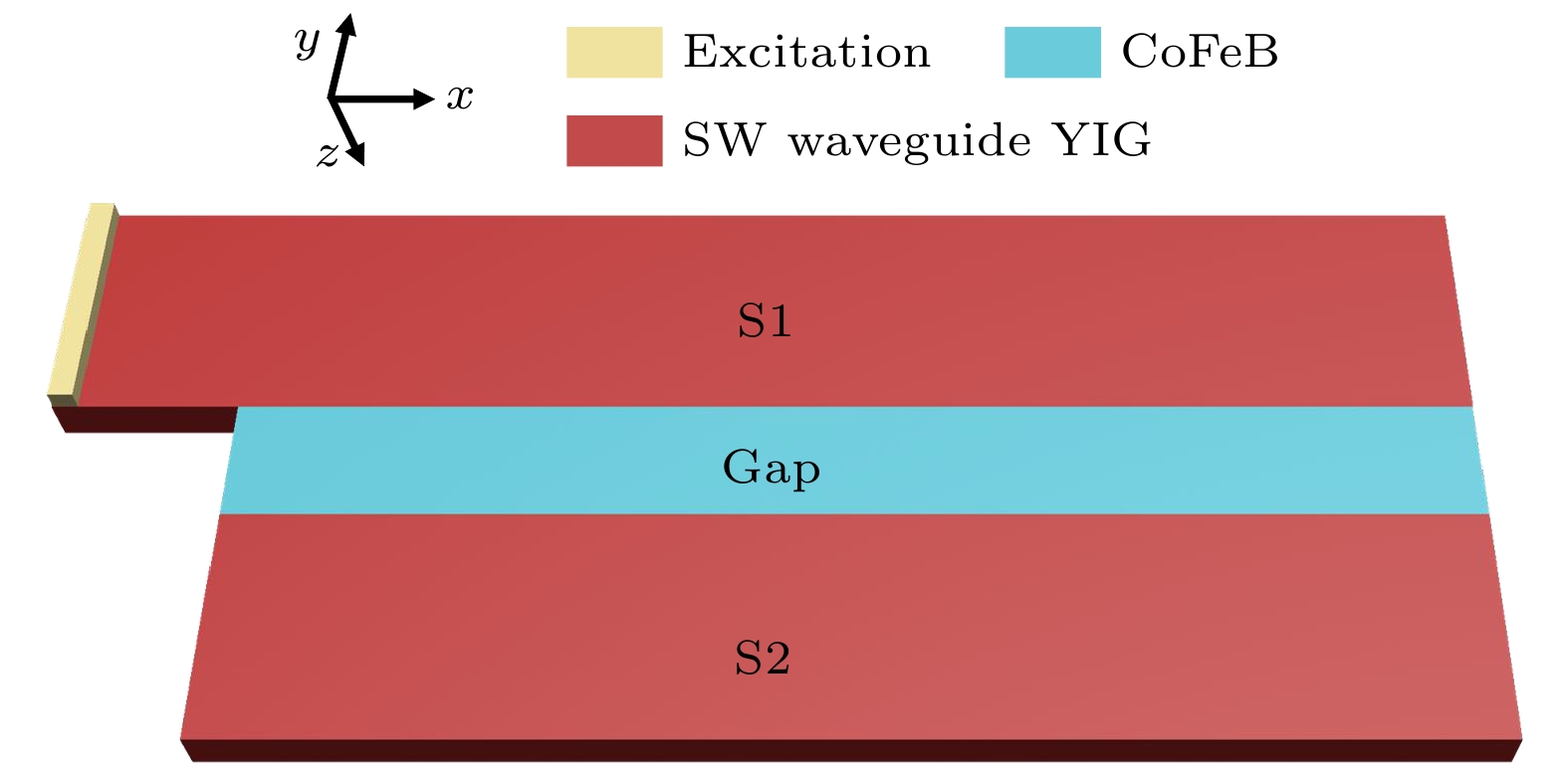 图 1 YIG-CoFeB自旋波定向耦合器结构示意图


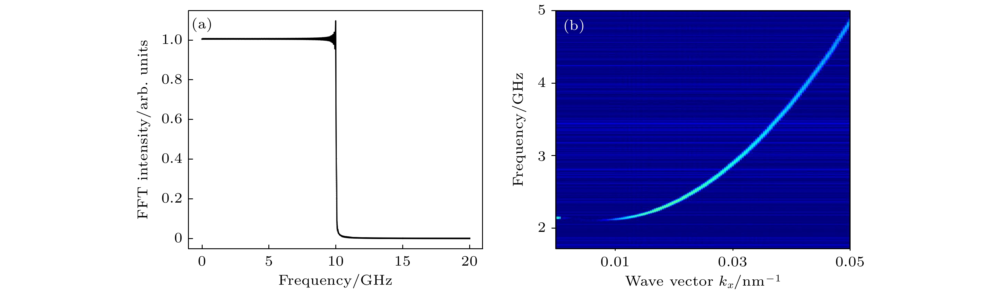 图 2 (a) 色散曲线求解中激励场在频域下的显示; (b) 孤立YIG波导中的色散曲线

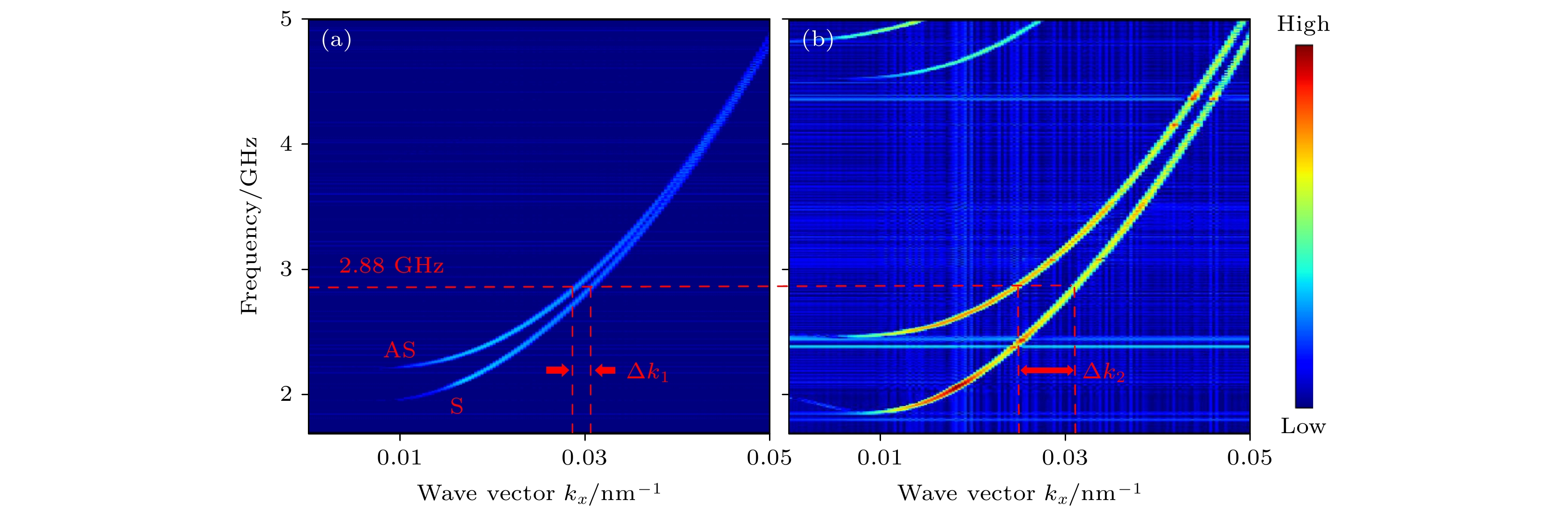 图 3 间隙处分别填充(a) Air和(b) CoFeB情况下的自旋波色散图


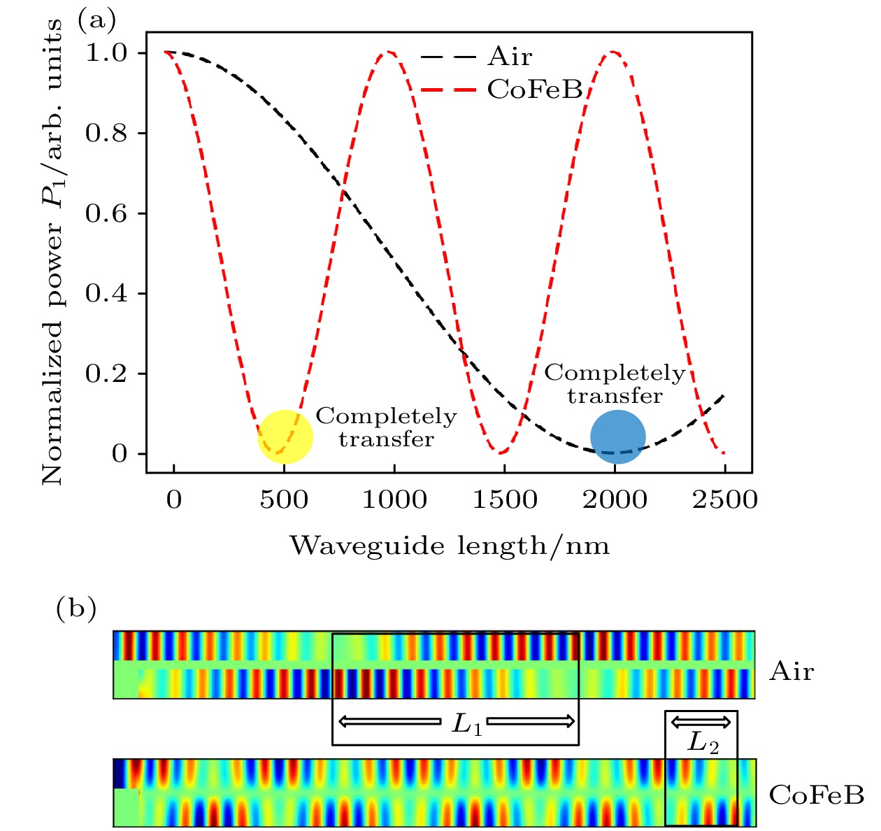 图 4 (a) 定向耦合器的输出随着波导长度变化的关系图; (b) 2.88 GHz下间隙处填充Air和CoFeB的定向耦合器工作过程中自旋波传播彩图
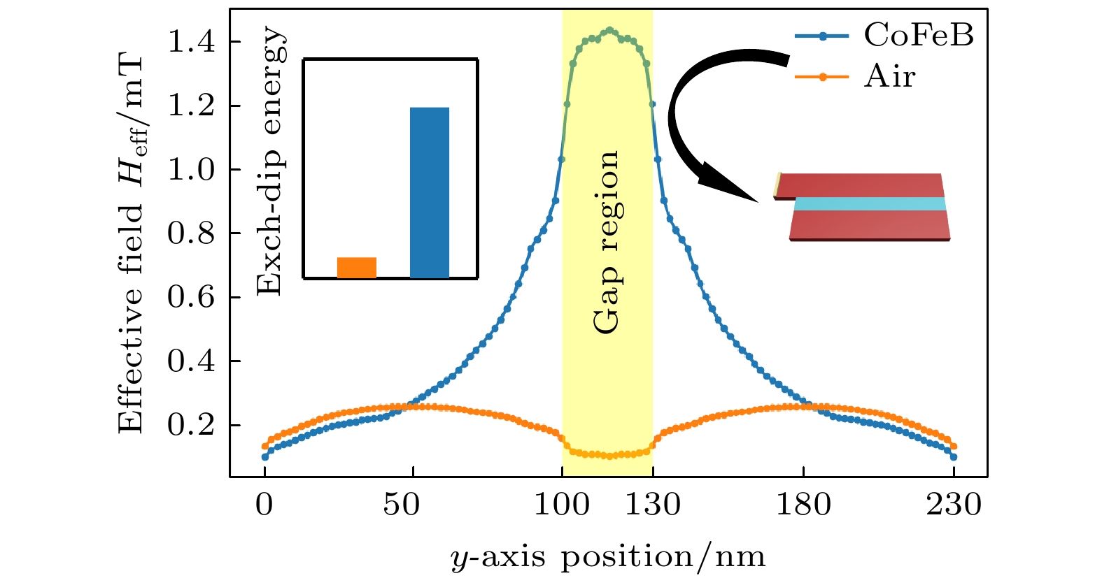 图 5 间隙处填充Air和CoFeB的定向耦合器中内部有效场分布
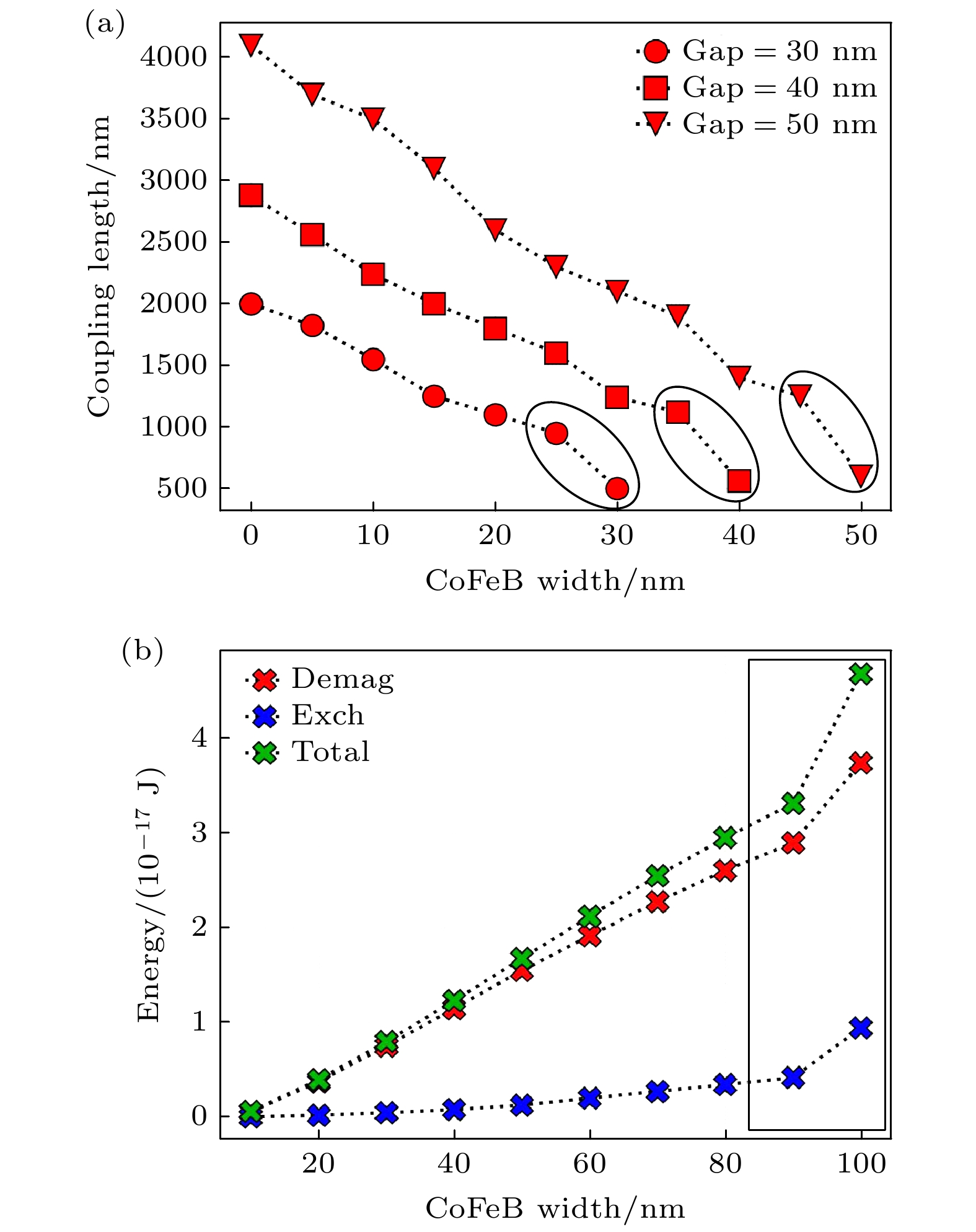 图 6 (a) 耦合长度随CoFeB宽度的变化; (b) 不同CoFeB宽度下器件的内部能量值
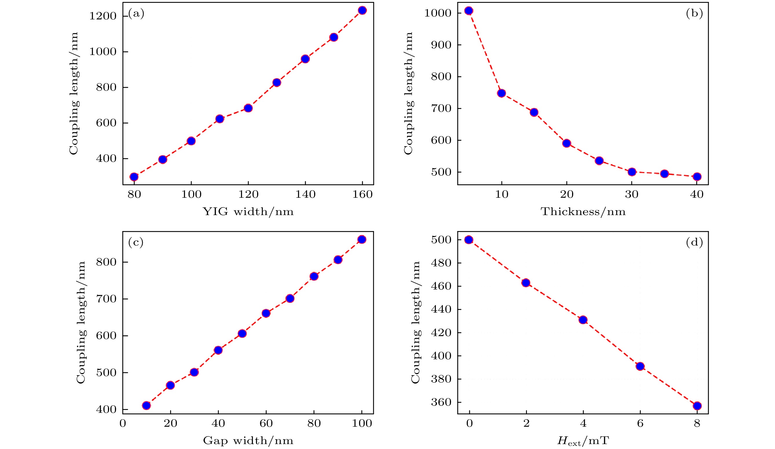 图 7 耦合长度随着(a) YIG波导宽度、(b) 波导厚度、(c) 间隙宽度和(d) 外磁场的变化


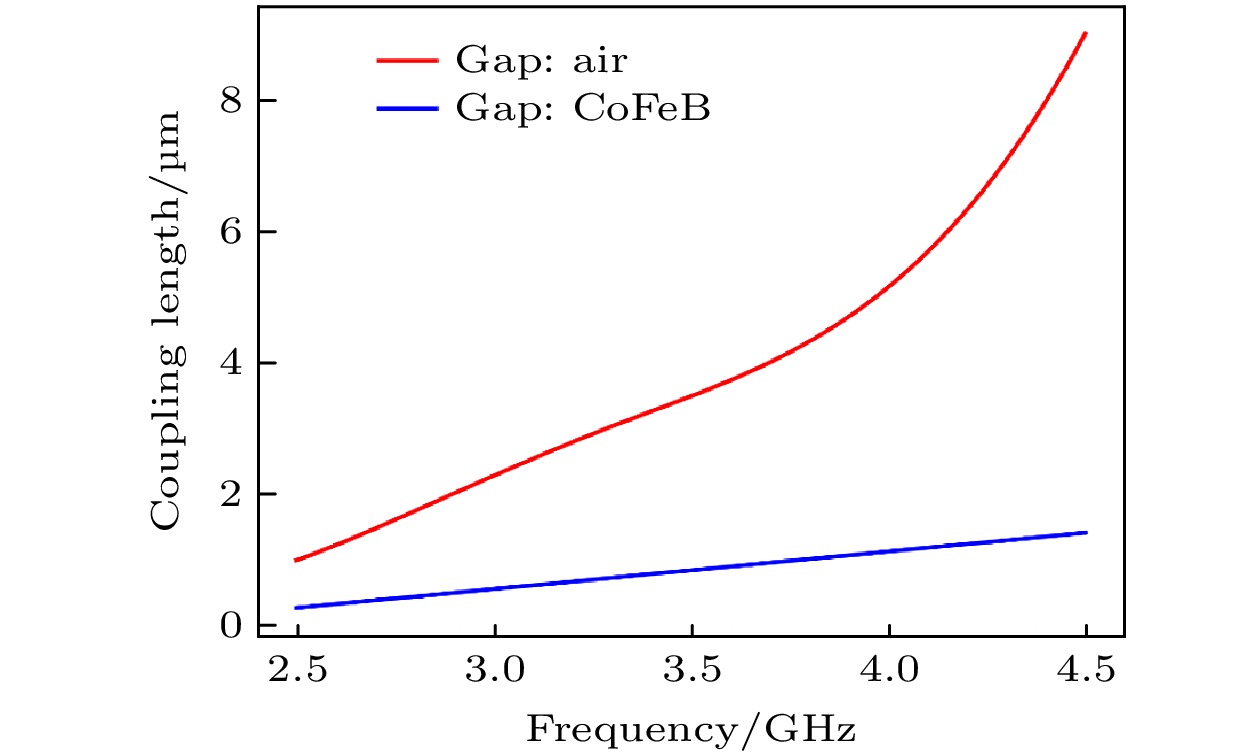 图 8 不同频率下定向耦合器的耦合长度