1.Hunan Key Laboratory for Super-Microstructure and Ultrafast Process, School of Physics and Electronics, Central South University, Changsha 410083, China 2.School of Physics and Electronic Sciences, Changsha University of Science and Technology, Changsha 410114, China 3.State Key Laboratory of Powder Metallurgy, Powder Metallurgy Research Institute, Central South University, Changsha 410083, China
Fund Project:Project supported by the National Natural Science Foundation of China (Grant Nos. 52073308, 11804395), the Distinguished Young Scholar Foundation of Hunan Province, China (Grant No. 2015JJ1020), and the Central South University Research Fund for Sheng-Hua Scholars, China (Grant No. 502033019)
Received Date:05 February 2021
Accepted Date:27 March 2021
Available Online:07 June 2021
Published Online:20 August 2021
Abstract:Monolayer tellurene is a novel two-dimensional semiconductor with excellent intrinsic properties. It is helpful in understanding doping and scattering mechanism to study the electronic structure of defective tellurene, thus it is important for the application of tellurene in electronic and photo-electronic devices. Using first-principles calculation based on the density functional theory, we investigate the effects of commonly seen point defects on the electronic structure and optical properties of monolayer β-Te. Seven kinds of point defects that may be present in β-Te are designed according to the lattice symmetry, including two single vacancies (SV-1, SV-2), two double vacancies (DV-1, DV-2) and three Stone-Wales (SW) defects (SW-1, SW-2, SW-3). It is found that the defect formation energies of these defects are 0.83–2.06 eV, which are lower than that in graphene, silicene, phosphorene and arsenene, suggesting that they are easy to introduce into monolayer β-Te. The two most stable defects are SV-2 and SW-1 where no dangling bond emerges after optimization. The calculated band structures show that all seven defects have little effect on the band gap width of monolayer β-Te, but they can introduce different numbers of impurity energy levels into the forbidden band. Among them, the SV-1, SV-2, DV-1 and SW-2 each act as deep level impurities which can be recombination centers and scattering centers of carriers, SW-1 acts as a shallow level impurity, DV-2 and SW-3 act as both deep level impurity and shallow level impurity. Besides, SW-1, SW-2 and DV-1 can change the band gap of monolayer β-Te from direct band gap to indirect band gap, which may result in the increase of the lifetime of carriers and decrease of photoluminescence of monolayer β-Te. The optical properties of monolayer β-Te, which are sensitive to the change in band structure, are also affected by the presence of defects. New peaks are found in the complex dielectric function and the absorption coefficient of defective monolayer β-Te in an energy range of 0–3 eV, of which the number and the position are dependent on the type of defect. The SV-1, DV-1, DV-2 and SW-2 can enhance the light response, polarization ability and light absorption in the low energy region of monolayer β-Te. This research can provide useful guidance for the applications of β-Te in the electronic and optoelectronic devices. Keywords:first-principle/ defective tellurene/ electronic structure/ optical properties
全文HTML
--> --> --> 1.引 言2004年, Novoselov等[1]通过机械剥离法得到单层石墨烯, 打开了通向二维材料研究领域的大门. 之后, 一系列二维材料体系被实验和理论科学家广泛研究, 例如硅烯[2]、锗烯[3]、锡烯[4]、磷烯[5]、锑烯[6]和过渡金属硫化物[7-9]等. 2017年, 研究人员通过理论计算和实验制备发现二维单层结构的碲单质—碲烯, 为二维材料家族增加了一个新成员[10]. 二维碲烯有三种层状结构, 分别是类二硫化钼1T相的α相(α-Te), 四方结构的β相(β-Te) 和类二硫化钼1H相的γ相(γ-Te), 可以实现不同的电子学功能. 目前, 实验上已尝试物理气相沉积[11]、溶液法合成[12]、范德瓦耳斯或分子束外延生长[13,14]、液相剥离[15]及热蒸镀[16]等多种方法制备二维碲烯, 发现其是带隙可调、迁移率高、热电优值大及结构稳定的半导体材料[17], 在电子和光电器件方面有重大应用潜力. 在单层极限下, 二维β-Te是稳定性好、禁带宽度适中、迁移率高的结构相, 因而受到特别关注. 二维碲烯相结构的稳定性依赖于材料厚度或层数, 两层以上最稳定的结构是α相, 减至单层时α相会转变为β相[18]. 理论研究显示, 单层β-Te是直接带隙半导体, 不同理论方法预测的带隙在1.03—1.79 eV之间, 室温下可具有高达几千cm2·V–1·s–1的载流子迁移率[10]. 实验上, Wang等[12]制备了横向尺寸100 μm、厚度为10—100 nm的高质量二维碲烯样品, 其场效应晶体管室温下能在空气中稳定存在2个月, 表现出高达106的开关比和700 cm2·V–1·s–1的高温载流子迁移率. 与之相比, 黑磷[19]晶体管虽有近1000 cm2·V–1·s–1的载流子迁移率, 但在空气中仅能稳定存在50 h, MoS2[20]和MoSe2[21]场效应晶体管分别能在空气中存在3个月和21天, 但迁移率只有约25 cm2·V–1·s–1和35 cm2·V–1·s–1. 因此, 二维碲烯在一定程度上可弥补石墨烯、黑磷及过渡金属硫化物等二维材料应用于场效应晶体管中表现的不稳定性和性能缺陷. 除电子性质优异之外, 研究表明二维碲烯还具有优异的光学性质[22]和热电性质[23], 在光探测器、偏振光传感器及能源器件中具有实用价值. 实验上可通过多种方法制备二维碲烯, 样品质量与所选制备工艺、化学环境密切相关, 研究二维β-Te结构与电子结构的关系也因此成为一个重要问题. 二维β-Te虽有优异的本征电子学性质, 但其所有原子都处于表面, 容易形成缺陷结构(包括空位、吸附原子、取代、间隙和拓扑缺陷[24]), 性质也易受缺陷影响而发生改变. 在材料制备过程中, 缺陷结构的出现通常是不可避免的. 例如, 在淬火或受到辐射时石墨烯中会产生Stone Wales(SW) 缺陷[25], 在CVD生长时二维MoS2的晶格会缺失原子形成空位缺陷[26]. 缺陷破坏材料的晶格周期性, 构成载流子的散射中心或复合中心, 形成化学活性位点, 影响半导体材料的电子结构及相关应用[27,28]. 实际应用中, 一方面需要估计缺陷对二维材料性质产生的可能影响, 一方面需探索利用缺陷进行能带调控实现新材料的设计. 例如, 理论计算显示单空位缺陷可给MoS2引入磁性并提高它的激子效率[29-31], Te空位缺陷使单层1${\rm{T}}' $相MoTe2出现带隙[32]. 在发现二维β-Te优异的本征电子学性质之后, 研究缺陷二维β-Te的电子结构也自然成为必要. 目前, 虽有工作报道吸附原子和分子的单层β-Te的电子性质[33], 但对空位缺陷、SW缺陷的单层β-Te仍少见报道. 因此, 本文基于第一性原理电子结构计算方法, 对含空位、SW缺陷等7种可能缺陷结构的单层β-Te的电子结构和光学性质进行系统研究, 分析并讨论了缺陷结构对单层β-Te结构稳定性、电子能带结构、复介电函数和光学吸收系数的影响, 研究结果有助于加深对单层β-Te电子性质的理解, 指导相关材料与器件的设计和制备. 2.计算模型与方法单层β-Te的几何结构如图1(a)所示, 它由交替排列在波状结构上的四元环和椅型六元环构成, 包含位于3个不同平面的原子层. 单层β-Te的晶格是二维的四方晶格, 本文对单层β-Te进行优化后得到晶格常数a = 4.21 ?和b = 5.71 ?, 接近实验给出的a = 4.26 ?和b = 5.42 ?[14]. 为研究缺陷效应, 本文根据原子位置的对称性在4 × 6的单层β-Te超晶格中构造了7种常见点缺陷结构, 优化后缺陷周围的原子结构如图1(b)—(h)所示. 在单层β-Te的3个原子层中, 中间层的Te原子位点与上下两层的Te原子位点不等价. 图1(b)和图1(c)给出这两种不等价位点缺失形成的单空位缺陷结构. 为了方便, 本文参考了文献中的方法为所有缺陷结构定义简称[34-39]. 缺失中间层Te原子的单空位缺陷简记为SV-1, 缺失上层或下层Te原子的空位缺陷简记为SV-2. 图1(d)是单层β-Te缺失相邻六元环共有的2个原子所形成的双空位缺陷, 简记为DV-1, 图1(e)是单层β-Te缺失相邻四元环和六元环共有的2个原子所形成的双空位缺陷, 简记为DV-2. SW缺陷是通过旋转晶体中化学键所形成的一种拓扑缺陷结构. 以通过旋转键的中心并垂直原子平面的直线作旋转轴, 根据旋转化学键的位置和旋转方式可在单层β-Te中得到三种SW缺陷结构. 图1(f)中所示的SW缺陷是90°旋转单层β-Te中2个六元环共有的化学键得到的结构, 该缺陷周围有4个五元环, 简记为SW-1. 四元环与六元环共有的化学键与原子平面有夹角, 沿不同方向旋转该化学键得到不同结构. 图1(g)是90°逆时针旋转四元环与六元环共有化学键得到的SW缺陷, 周围有1个三元环、2个五元环和1个七元环, 简记为SW-2. 图1(h)是90°顺时针旋转四元环与六元环共有化学键得到的SW缺陷, 周围有1个三元环、1个五元环、1个七元环和1个九元环, 简记为SW-3. 图 1 优化后单层β-Te的俯视图和侧视图 (a) Perfect; (b) SV-1; (c) SV-2; (d) DV-1; (e) DV-2; (f) SW-1; (g) SW-2; (h) SW-3. 红色虚线矩形表示晶格常数为a和b的原胞, 黑色矩形表示第一布里渊区, 绿色标记缺陷附近的原子, 红色标记SW缺陷结构中的旋转键 Figure1. Top and side views of optimized monolayer β-Te: (a) Perfect; (b) SV-1; (c) SV-2; (d) DV-1; (e) DV-2; (f) SW-1; (g) SW-2; (h) SW-3. The red dotted rectangle represents the unit cell with lattice constants a and b, and dark rectangle represents the first Brillouin zone. Green marks the atoms at the vicinity of defects, and red marks the rotating bonds in SW defects.
表1点缺陷形成能在单层β-Te与其他二维单质材料中的对比. 能量单位为eV.* Table1.The comparison of formation energies of various point defects in monolayer β-Te and other two-dimensional monoelemental materials. The unit of energy is eV.*
为了研究缺陷对单层β-Te电子结构的影响, 本文计算了含缺陷单层β-Te的能带结构、态密度, 并分析了缺陷态的波函数. 单层β-Te的能带和态密度如图2所示. 无缺陷时, 单层β-Te是直接带隙半导体, 带隙为1.23 eV, 和之前报道的带隙数值1.17 eV相当[8]. 引入缺陷后, 单层β-Te的带隙在1.16 eV到1.29 eV之间. 与无缺陷的情况相比, 缺陷引起单层β-Te的带隙变化很小. 其中, 稳定性最好的SV-2和SW-1的带隙增加了20 meV, 带隙变化最大的DV-1结构仅减小了70 meV, 说明缺陷对单层β-Te带隙的调控作用较弱. 这与缺陷对磷烯电子能带结构的影响类似[35], 可归因于缺陷周围Te原子贡献的占据态和未占据态分别接近于远离缺陷Te原子贡献的占据态和未占据态. 图 2 能带和态密度 (a) Perfect; (b) SV-1; (c) SV-2; (d) DV-1; (e) DV-2; (f) SW-1; (g) SW-2; (h) SW-3, 字母“f ”和红色数字分别标记缺陷能级和带隙 Figure2. Band structure and density of states: (a) Perfect; (b) SV-1; (c) SV-2; (d) DV-1; (e) DV-2; (f) SW-1; (g) SW-2; (h) SW-3. The defect-induced energy levels and band gaps are marked by the label “f ” and red numbers, respectively.
复介电函数实部$ {\varepsilon }_{1}\left(\omega \right) $反映了半导体材料在外电场中的极化程度, $ {\varepsilon }_{1}\left(\omega \right) $越大代表极化能力越强, 其中光子能量为0 eV时的$ {\varepsilon }_{1}\left(\omega \right) $称为静态介电常数. 入射光子能量在0—3 eV时, 单层β-Te的$ {\varepsilon }_{1}\left(\omega \right) $如图4所示. 由于单层β-Te结构的各向异性, x方向和y方向的$ {\varepsilon }_{1}\left(\omega \right) $不一致. 计算结果显示, 完整单层β-Te在x方向有2个峰Ax1 (位于1.53 eV)和Ax2 (位于2.48 eV), 在y方向有1个峰Ay (位于1.53 eV). x和y方向的静态介电常数分别是2.50和2.75. 引入缺陷后, 3个峰的能量位置几乎不变, 峰值有所减小. 但在其他能量位置出现新峰. 表2给出了不同缺陷的静态介电常数和新峰的能量位置. 由(3)式和(4)式可知, 出现在$ {\varepsilon }_{1}\left(\omega \right) $中的新峰是由缺陷单层β-Te的能带结构所决定的, 与缺陷类型密切相关. SV-1, DV-1, DV-2及SW-2中新峰出现的最小能量坐标分别是0.28, 0.58, 0.38和0.19 eV, 低能区$ {\varepsilon }_{1}\left(\omega \right) $和静态介电常数有明显增大. 相比于它们, SV-2和SW-1中新峰的位置分别在1.02 eV和1.21 eV, 低能区$ {\varepsilon }_{1}\left(\omega \right) $的变化较小. 由于能量较低, SV-2比SV-1对低能区的影响更大, 静态介电常数在x方向和y方向比SV-1分别高0.09和0.17. SW-3没有呈现新峰, 其低能区$ {\varepsilon }_{1}\left(\omega \right) $几乎不受影响. 这说明, 单层β-Te材料在低能区的极化能力将与材料中主要缺陷的类型密切相关. 根据静态介电常数的计算结果, 稳定性最好的两类缺陷SV-2和SW-1对单层β-Te极化能力有轻微增强作用. 图 4 复介电函数实部 (a) Perfect; (b) SV-1; (c) SV-2; (d) DV-1; (e) DV-2; (f) SW-1; (g) SW-2; (h) SW-3, 蓝色和深青色分别表示x和y方向, A标记主峰, B标记缺陷峰, 虚线是完整单层的复介电函数实部 Figure4. The real part of dielectric function: (a) Perfect; (b) SV-1; (c) SV-2; (d) DV-1; (e) DV-2; (f) SW-1; (g) SW-2; (h) SW-3. The blue and dark cyan curves represent x and y directions, respectively. The main peaks are marked by A and the defect-induced peaks are marked by B, and the dotted lines are the real part of dielectric function of perfect monolayer.
perfect
SV-1
SV-2
DV-1
DV-2
SW-1
SW-2
SW-3
静态介电常数
x方向
2.50
3.41
2.71
2.96
2.83
2.62
2.98
2.52
y方向
2.75
3.60
2.98
3.27
3.29
2.81
3.62
2.84
缺陷峰坐标/eV
x方向
—
0.28
1.02
—
0.48, 1.01
1.21
0.19, 0.46
—
y方向
—
0.28
1.02
0.58
0.38, 0.69, 1.01
—
0.19, 0.46
—
表2静态介电常数和复介电函数实部中缺陷峰的能量 Table2.Static dielectric constant and defect peak energy coordinate of the real part curve.
复介电函数的虚部ε2(ω)表示半导体内部形成电偶极子时所消耗的能量, 决定材料在较小波矢下对光的线性响应. 入射光子能量在0—3 eV时, 单层β-Te的ε2(ω)如图5所示, 无缺陷单层β-Te的ε2(ω)在x方向有2个峰, Ax1位于1.72 eV, Ax2位于2.61 eV. 在y方向有1个峰, Ay位于1.72 eV. 引入缺陷后, Ax1, Ax2和Ay的峰值都减小, 峰Ax1稍微蓝移, Ax2和Ay位置几乎不变. 峰的能量位置变化很小的主要原因是缺陷对单层β-Te的带隙影响较小. 根据缺陷类型, ε2(ω)也出现不同数量的新峰, 新峰的能量坐标如表3所示. SV-1, DV-1, DV-2及SW-2中在小于1.00 eV的能量范围出现了新的ε2(ω)峰, 说明它们能够提高单层β-Te在低能区的光响应. SV-2的ε2(ω)新峰对应能量为1.12 eV, 接近其ε1(ω)新峰的位置. 由于SV-2的ε2(ω)新峰较宽, 该类缺陷对低能区光响应有一定提高. SW-1中的ε2(ω)只在1.20 eV左右比完整结构的ε2(ω)大, SW-3没有新峰, 两类缺陷对单层β-Te在低能区的光响应影响很弱. 图 5 复介电函数虚部 (a) Perfect; (b) SV-1; (c) SV-2; (d) DV-1; (e) DV-2; (f) SW-1; (g) SW-2; (h) SW-3, 蓝色和深青色分别表示x和y方向, A标记主峰, B标记缺陷峰, 虚线是无缺陷的单层β-Te的复介电函数虚部 Figure5. The imaginary part of dielectric function: (a) Perfect; (b) SV-1; (c) SV-2; (d) SW-1; (e) SW-2; (f) SW-3; (g) DV-1; (h) DV-2. The main peaks are marked by A and the defect-induced peaks are marked by B, and the dotted lines are the imaginary part of dielectric function of perfect monolayer.
SV-1
SV-2
DV-1
DV-2
SW-2
x方向/eV
0.09, 0.39
1.12
0.06
0.71, 1.15
0.22, 0.55
y方向/eV
0.52
1.12
0.66
0.83
0.22, 0.55
表3复介电函数虚部中缺陷峰的能量坐标 Table3.Energies coordinates of defect-induced peaks in the imaginary part of dielectric function.
ε2(ω)与缺陷类型之间的关系可由光吸收选择定则和缺陷单层β-Te的电子结构给出定性的解释. (3)式指出, ε2(ω)只在入射光子能量$ \hslash \omega $等于未占据态本征能量与占据态本征能量的差值时才不为0, 这是光吸收的能量守恒定则. 根据这一定则, 在带隙中引入缺陷能级后, ε2(ω)可在$ \hslash \omega $等于费米能上导带或缺陷态能量减去费米能下缺陷态或价带能量时有值. 因此, 与完整的单层β-Te相比, 缺陷单层β-Te在低于带隙的能量范围内出现有一定大小且与缺陷能级位置和展宽有关的ε2(ω). 其中, SW-1引入的两条缺陷能级分别靠近导带底与价带顶, 缺陷态与缺陷态之间的能量差接近带隙, 因此其ε2(ω)在1.20 eV能量附近增大. SW-3除引入的两条浅缺陷能级之外, 还有一条深缺陷能级. 但是其深缺陷能级近乎平直, 对应态密度峰十分尖锐, 布洛赫波函数也比其他缺陷态更加局域, 可能导致(3)式中的积分项很小, 因此SW-3对低能区的ε2(ω)影响很小. 由于(4)式和(5)式, ε1(ω)和$ \alpha \left(\omega \right) $与缺陷类型之间的关系类似于ε2(ω). 为进一步了解缺陷单层β-Te的光学性质, 计算了入射光子能量为0—3 eV时单层β-Te的光吸收系数, 如图6所示. 光吸收系数描述介质中单位距离光强度的衰减, 在单层β-Te中, 光吸收系数表现出明显的各向异性. 无缺陷单层β-Te的光吸收系数在x和y方向分别有2个峰. x方向的峰Ax1位于1.95 eV, Ax2位于2.73 eV. y方向的峰Ay1位于2.25 eV, Ay2位于2.60 eV. 计算的峰值高达105量级, 与之前的报道一致[8]. 如图6(a)—(h)所示, 引入缺陷后, 由于材料带隙变化很小, 这些吸收峰的位置近乎不变, 但峰值减小. 其中, SV-1, SW-1, SW-2和SW-3的峰Ay2, SW-3的峰Ax1甚至因峰值减小导致峰的特征消失. 此外, 缺陷引入了一些新的吸收峰. 经过分析, 这些吸收峰位置及其对应跃迁如表4所示. 结果显示, 这些新峰来自于缺陷能级之间或者缺陷能级与价带顶之间的跃迁. 与复介电函数的虚部一致, SV-1, DV-1, DV-2和SW-2四类缺陷对1.0 eV能量范围的吸收系数有一定增强, SV-2缺陷诱导吸收峰位于1.12 eV, SW-1和SW-3没有引入新的吸收峰, 对低能区光吸收影响很小, 由上可知, 引入缺陷会导致单层β-Te光吸收系数改变, 吸收系数与缺陷的类型相关. 由于实验上材料缺陷的出现难以避免, 不同制备方法所产生缺陷密度及类型亦不同, 因此单层β-Te光吸收系数敏感地依赖于材料制备工艺. 图 6 单层β-Te光学吸收系数 (a) Perfect; (b) SV-1; (c) SV-2; (d) DV-1; (e) DV-2; (f) SW-1; (g) SW-2; (h) SW-3. 蓝色和深青色分别表示x和y方向, A标记主峰, B标记缺陷峰, 虚线是完整单层的光学吸收系数 Figure6. The optical absorption coefficient of monolayer β-Te: (a) Perfect; (b) SV-1; (c) SV-2; (d) DV-1; (e) DV-2; (f) SW-1; (g) SW-2; (h) SW-3. The main peaks are marked by A and the defect-induced peaks are marked by B, and the dotted lines are the optical absorption coefficient of perfect monolayer.
缺 陷 峰
x方向
y方向
能量/eV
对应跃迁
能量/eV
对应跃迁
SV-1
0.38
f1→f2
0.63
价带顶→f2
SV-2
1.12
价带顶→ f1、f2
—
—
DV-1
—
—
0.72
价带顶→f2
SW-2
—
—
0.62
f1→f2, 价带顶→f2
表4光学吸收系数中缺陷峰的能量坐标和对应的跃迁 Table4.Energies coordinates of defect-induced peaks in absorption coefficient and corresponding transition between energy levels.

 图 1 优化后单层β-Te的俯视图和侧视图 (a) Perfect; (b) SV-1; (c) SV-2; (d) DV-1; (e) DV-2; (f) SW-1; (g) SW-2; (h) SW-3. 红色虚线矩形表示晶格常数为a和b的原胞, 黑色矩形表示第一布里渊区, 绿色标记缺陷附近的原子, 红色标记SW缺陷结构中的旋转键


 图 2 能带和态密度 (a) Perfect; (b) SV-1; (c) SV-2; (d) DV-1; (e) DV-2; (f) SW-1; (g) SW-2; (h) SW-3, 字母“f ”和红色数字分别标记缺陷能级和带隙
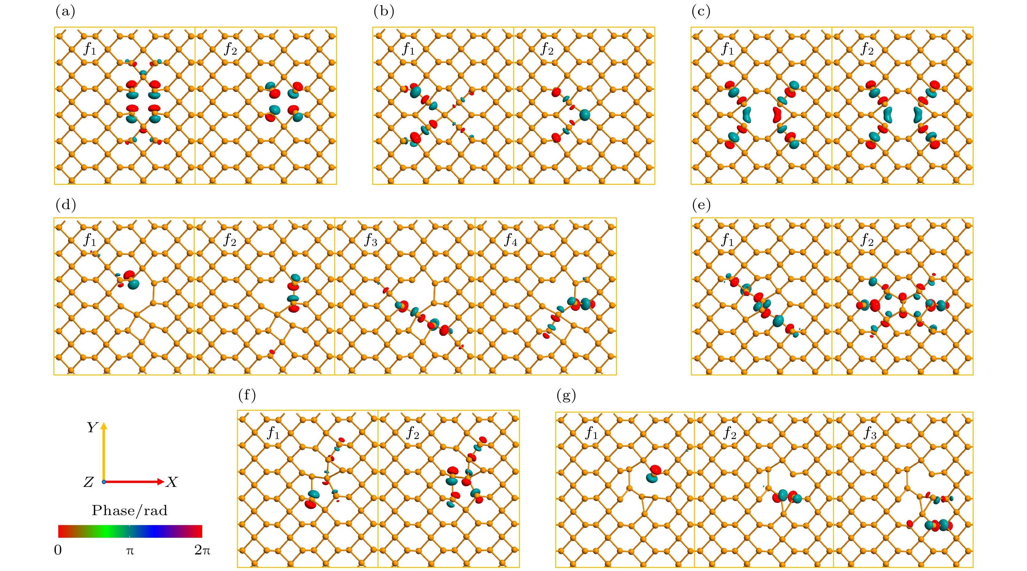 图 3 缺陷能级中的布洛赫态 (a) SV-1; (b) SV-2; (c) DV-1; (d) DV-2; (e) SW-1; (f) SW-2; (g) SW-3. f1, f2, f3表示图2中对应的能级


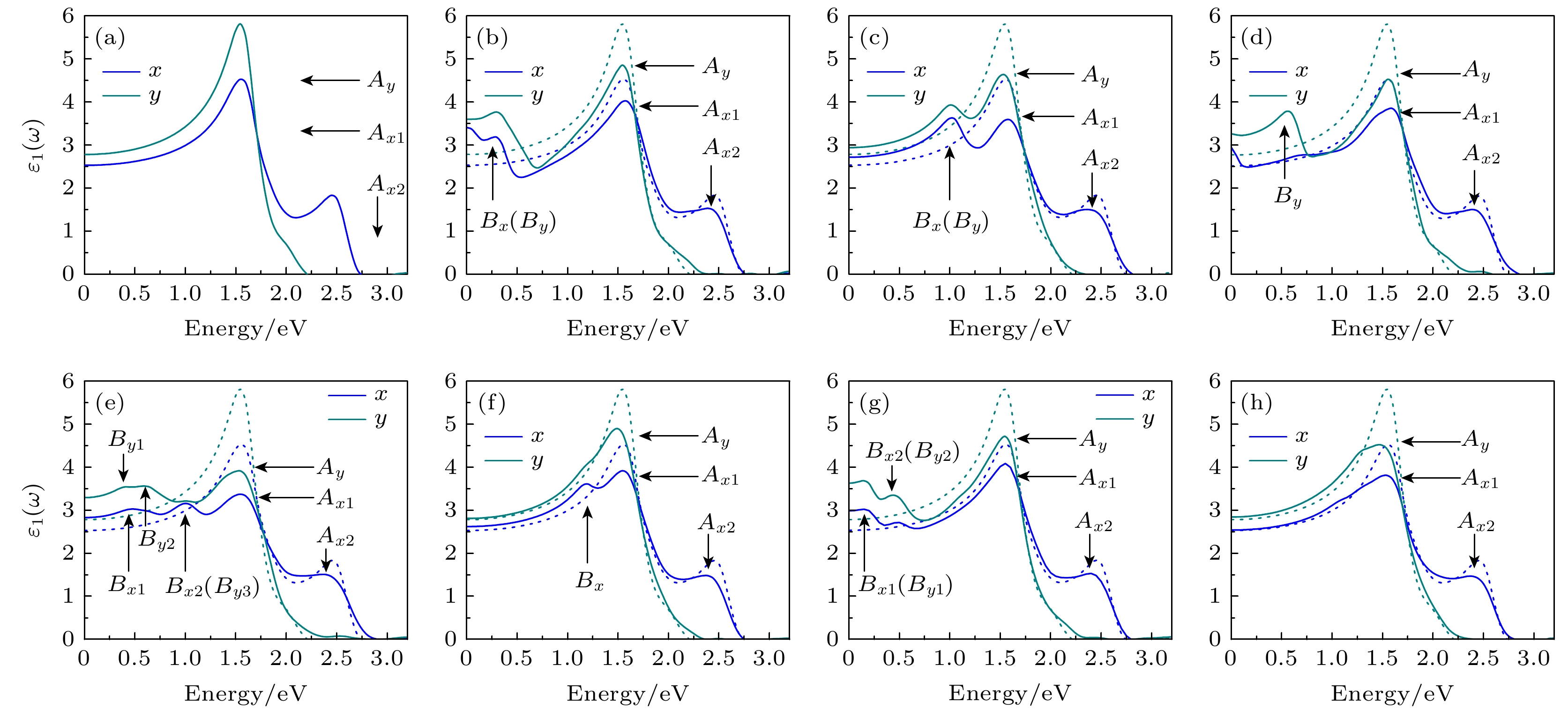 图 4 复介电函数实部 (a) Perfect; (b) SV-1; (c) SV-2; (d) DV-1; (e) DV-2; (f) SW-1; (g) SW-2; (h) SW-3, 蓝色和深青色分别表示x和y方向, A标记主峰, B标记缺陷峰, 虚线是完整单层的复介电函数实部
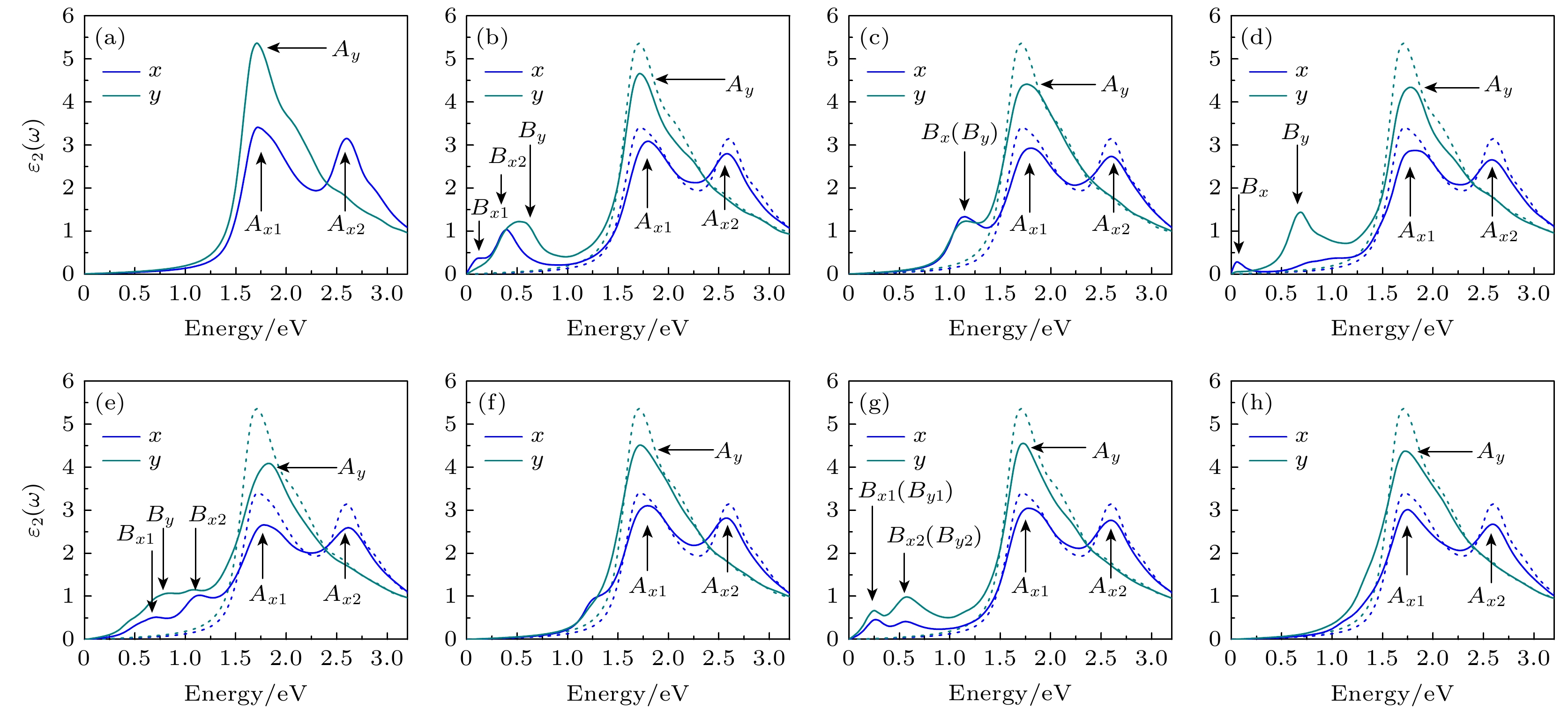 图 5 复介电函数虚部 (a) Perfect; (b) SV-1; (c) SV-2; (d) DV-1; (e) DV-2; (f) SW-1; (g) SW-2; (h) SW-3, 蓝色和深青色分别表示x和y方向, A标记主峰, B标记缺陷峰, 虚线是无缺陷的单层β-Te的复介电函数虚部


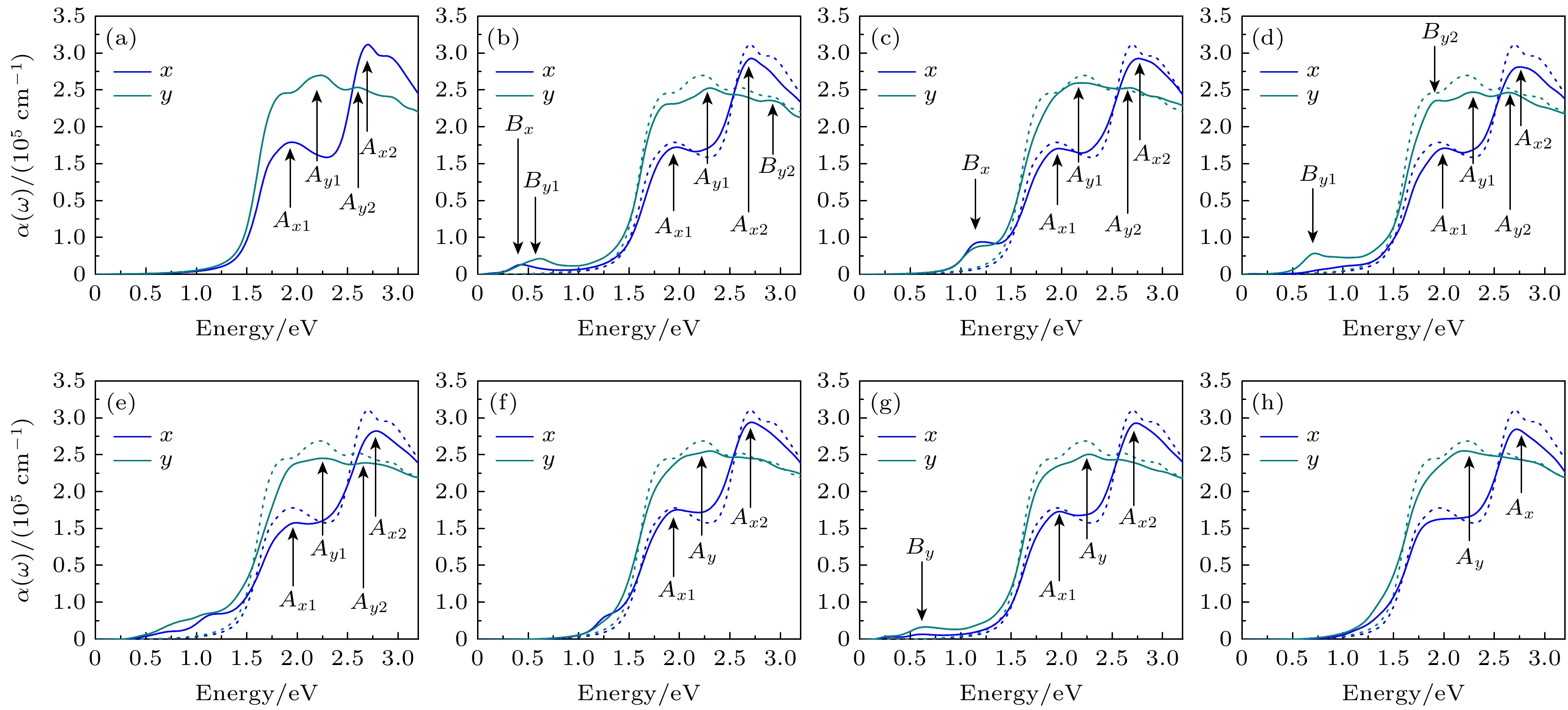 图 6 单层β-Te光学吸收系数 (a) Perfect; (b) SV-1; (c) SV-2; (d) DV-1; (e) DV-2; (f) SW-1; (g) SW-2; (h) SW-3. 蓝色和深青色分别表示x和y方向, A标记主峰, B标记缺陷峰, 虚线是完整单层的光学吸收系数