全文HTML
--> --> -->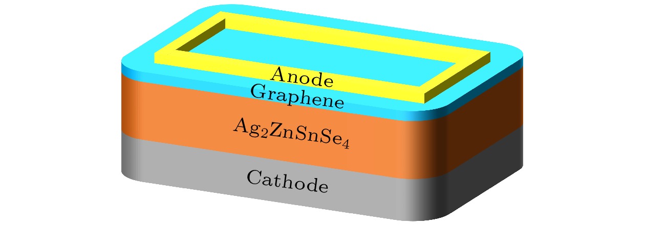 图 1 模拟器件结构
Figure1. Structure of the graphene/AZTSe induced p-n junction solar cell used in the numerical simulation.
| 参数 | AZTSe |
| 厚度/μm | 2 |
| 相对介电常数 εr | 12.6 |
| 电子亲和能 χe/eV | 4.2 |
| 禁带宽度 Eg/eV | 1.4 |
| 施主掺杂浓度 ND/cm–3 | 1011—1016 |
| 导带有效态密度 Nc /cm–3 | 2.2 × 10¹⁸ |
| 价带有效态密度Nv /cm–3 | 1.8 × 10¹⁹ |
| 电子迁移率 μn/cm2·V–1·s–1 | 100 |
| 空穴迁移率 μp/cm2·V-1·s–1 | 2 |
| 缺陷密度 Nt/cm–3 | 1013—1018 |
表1模拟使用的主要材料参数
Table1.Main material parameters used in the numerical simulation.
3.1.石墨烯功函数的影响
在Graphene/AZTSe诱导p-n结薄膜太阳电池中, 石墨烯不仅充当透明导电电极和太阳光进入电池的窗口层, 发挥载流子收集功能, 更重要的是诱导半导体吸收层表面发生反型, 直接参与光生载流子的分离, 因此石墨烯对诱导p-n结薄膜太阳电池性能有很大的影响. 早期研究报道石墨烯的功函数在3.40—5.14 eV之间[20-22], 最近Seo等[23]利用化学气相沉积的方法制备了功函数高达5.5 eV的石墨烯. 我们首先保持电池背接触为平带结构, 通过调整石墨烯的功函数来研究Graphene/AZTSe太阳电池的光伏性能. 图2(a)给出的是电池的电流密度-电压特性曲线, 可以看出, 随着功函数的增加, 电池的开路电压、短路电流和填充因子都得到明显改善, 功函数为5.5 eV时, 电池的开路电压、短路电流、填充因子和转换效率分别为856.4 mV, 31.28 mA/cm2, 84.04%和22.51%.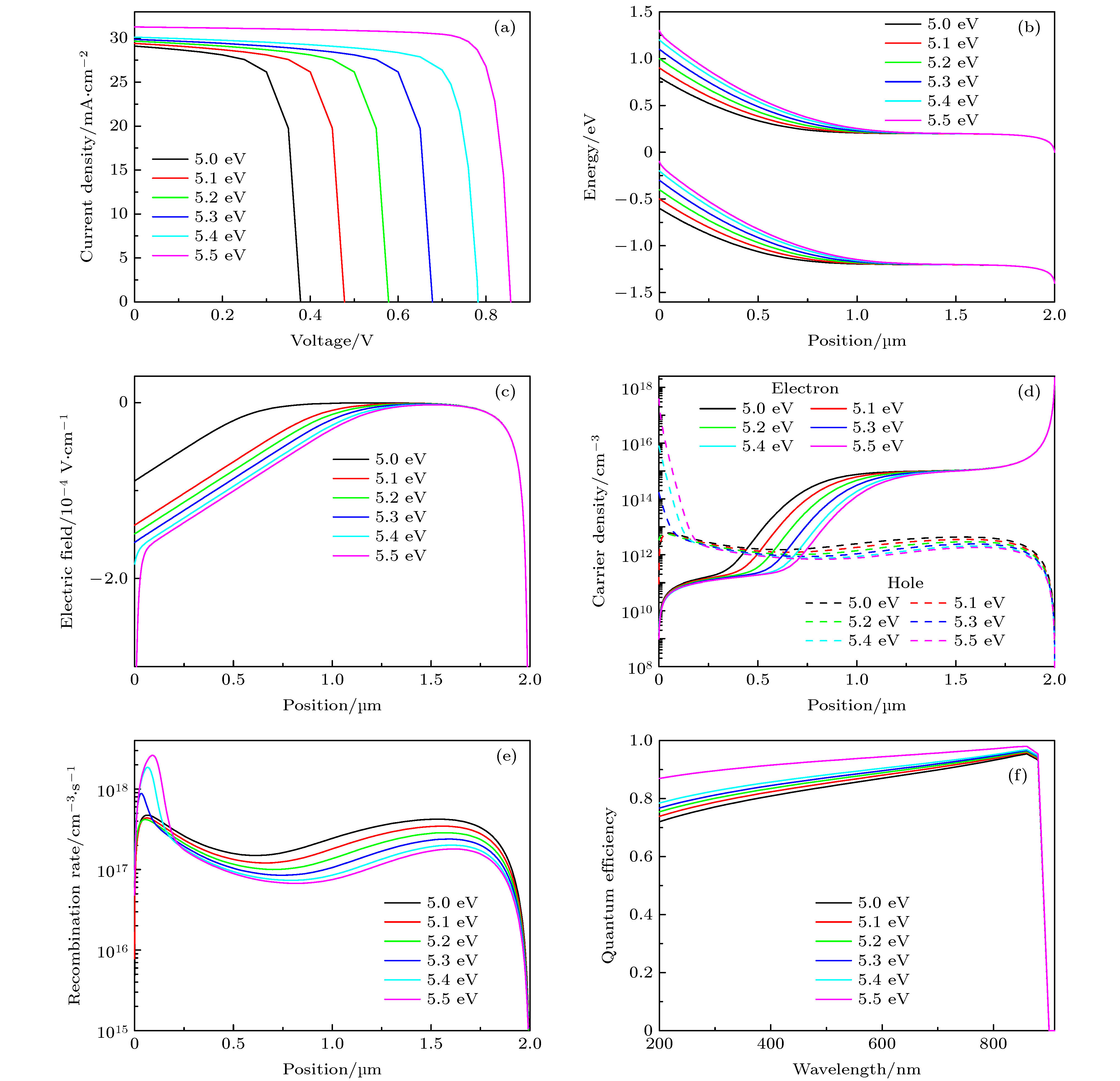 图 2 不同石墨烯功函数情况下电池的 (a)电流密度-电压特性曲线, (b)能带结构, (c)电场分布, (d)载流子浓度, (e)载流子复合率分布, (f)量子效率
Figure2. Graphene/AZTSe induced p-n junction thin film solar cell with different values of graphene work function (a) current density-voltage curves, (b) energy band structure, (c) electric field, (d) carrier concentration, (e) carrier recombination rate profile, (f) quantum efficiency.
为了更深入理解石墨烯功函数对电池性能改善的物理机理, 图2(b)给出了不同石墨烯功函数情况下的电池能带结构. 高功函数的石墨烯与(n)AZTSe吸收层接触时, 两种材料之间的费米能级差驱动着电子从(n)AZTSe吸收层流向石墨烯, (n)AZTSe吸收层前端的能带向上弯曲, 导带远离费米能级而价带靠近费米能级, 在(n)AZTSe吸收层前端诱导形成一个p型AZTSe反型层, p型AZTSe和n型AZTSe组成诱导p-n同质结. 在以n型MoOx作为空穴选择性接触的结构为TCO/(n)MoOx/(i)a-Si:H/(n)c-Si/(i)a-Si:H/(n)a-Si:H的硅异质结太阳电池中, 高功函数的n型MoOx与n型c-Si接触时同样引起c-Si表面的能带弯曲, 形成p型反型层和诱导p-n同质结[12,24,25], 而且取得了23.5%的效率[26]. 由图2(b)还可以看到, 随着石墨烯功函数的增加, (n)AZTSe吸收层前端能带弯曲程度增大, 越有利于光生载流子的分离, 从而提高电池的开路电压. 图2(b)中也可以看出石墨烯功函数的增加对电池背接触的能带结构几乎没有影响.
图2(c)给出了不同石墨烯功函数情况下电池的电场分布情况. 图中显示的(n)AZTSe吸收层前端负方向的电场也印证了前述的p型反型层. 石墨烯的功函数越大, 负方向的电场越大, 越有利于(n)AZTSe吸收层中光生载流子的分离和光生空穴向石墨烯输运从而被石墨烯收集.
图2(d)给出了不同石墨烯功函数情况下电池内的载流子分布情况. 由图可见(n)AZTSe吸收层前端的空穴浓度大于电子浓度, 再次印证了前述的p型反型层.随着功函数的增加, (n)AZTSe吸收层前端的空穴浓度增加, 说明(n)AZTSe吸收层前端的反型程度也在增强. 能带弯曲程度的增加和反型程度的增强有利于光生空穴流过Graphene/(n)AZTSe界面, 同时也会阻挡光生电子流向界面. 也就是说石墨烯功函数的增加有利于空穴选择性流过, 从而提高了Graphene/(n)AZTSe接触的载流子选择性, 改善了光生载流子的输运性能, 有利于提高电池的填充因子.
图2(e)给出了不同石墨烯功函数情况下电池内的载流子复合情况. 由图可见石墨烯功函数越大, (n)AZTSe吸收层前端的空穴浓度越高, 使得前端载流子的复合率越高. 不过整个(n)AZTSe吸收层中则是石墨烯功函数越大, 载流子复合率越小.
图2(f)给出了不同石墨烯功函数情况下电池的量子效率. 由图可见石墨烯功函数越大, 光生载流子的分离和收集越有效, 载流子复合率越小, 电池的量子效率越高, 从而改善了电池的整体性能.
2
3.2.背接触功函数的影响
背接触主要影响太阳电池背端的能带结构和光生载流子的收集, 对太阳电池的性能也有很大影响. 接下来的模拟是在保持石墨烯功函数为5.5 eV不变的情况下进行的, 背接触功函数的变化区间选择在3.8—5.0 eV之间. 图3(a)显示的是模拟所得太阳电池的电流密度-电压特性曲线, 可以看到, 背接触功函数为3.8 eV时电池的效率可以进一步提升到22.59%. 当背接触功函数从3.8 eV增加到4.4 eV, 电池性能变化很小, 当功函数继续增加, 电池性能明显下降, 并且主要是电池的开路电压明显变差. 图3(b)显示的是不同背接触功函数时电池的能带结构. 当背接触功函数小于4.4 eV时, 功函数影响的是(n)AZTSe吸收层背部近表面区域, 并且功函数小于4.4 eV时能带向下弯曲, 光生电子能够被背接触高效收集. 当功函数继续增加, 由于器件为薄膜太阳电池, 功函数的影响向AZTSe吸收层前端延伸, 能带弯曲程度下降, 电池开路电压下降. 同时背部的能带向上抬升, 光生电子收集受阻, 影响载流子的输运特性进而影响电池的填充因子. 受阻的电子不能流过(n)AZTSe/背接触界面, 在界面处电子浓度急剧下降, 如图3(c)所示. 而背接触功函数越小, 电子浓度越高, 容易在背接触界面附近积累, 使得载流子复合率升高, 如图3(d)所示.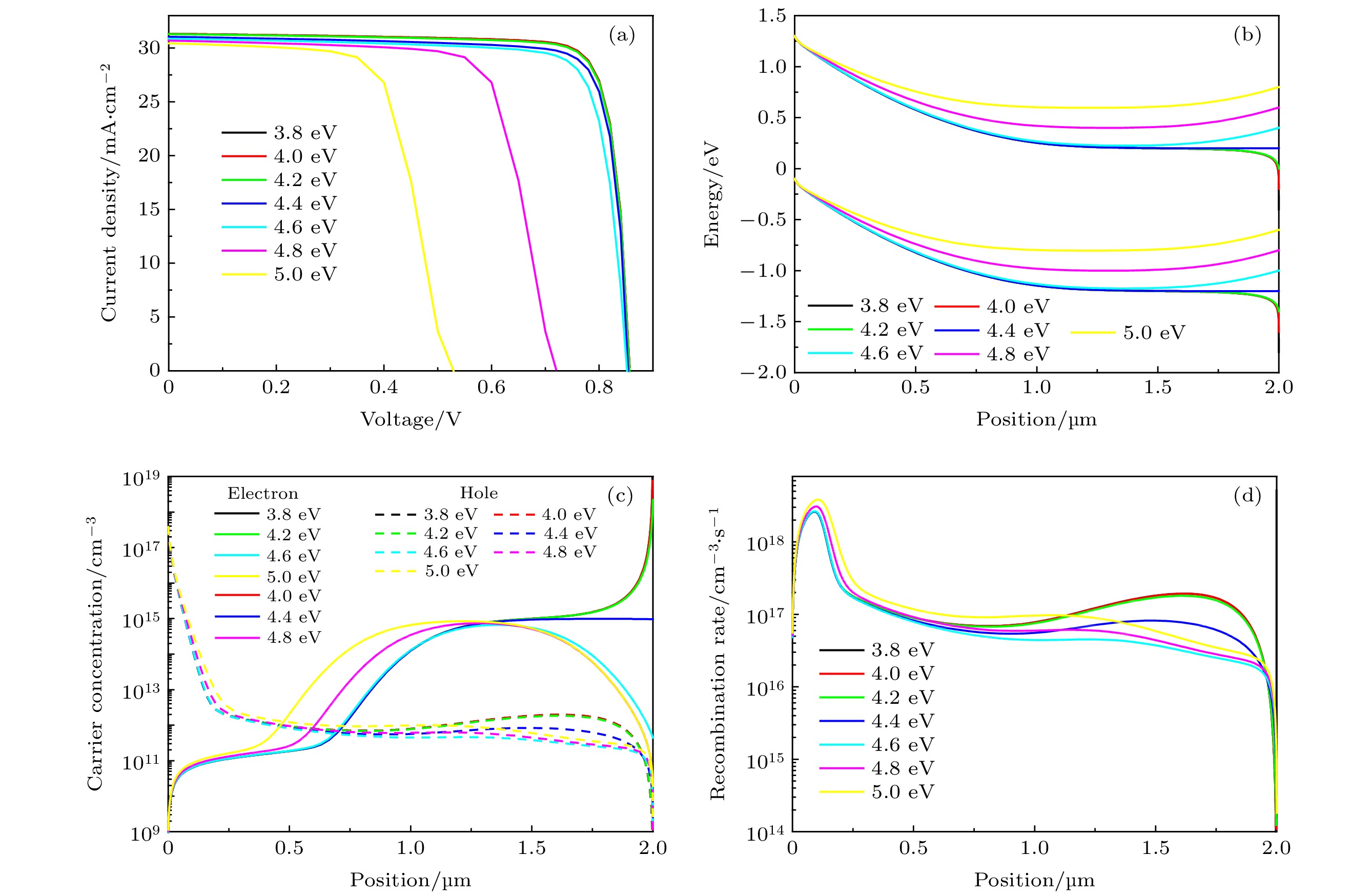 图 3 不同背接触功函数时电池的 (a)电流密度-电压特性曲线, (b)能带结构, (c)电子浓度, (d)载流子复合率分布
Figure3. Graphene/AZTSe induced p-n junction thin film solar cell with different values of back contact work function (a) current density-voltage curves, (b) energy band structure, (c) carrier concentration, (d) carrier recombination rate profile.
2
3.3.吸收层掺杂浓度的影响
继续模拟AZTSe吸收层掺杂浓度对电池性能的影响, 模拟时石墨烯和背接触的功函数分别为5.5和3.8 eV, 掺杂浓度从1010 cm–3增加到1016 cm–3. 不同吸收层掺杂浓度情况下电池的电流密度-电压特性曲线如图4所示. 可以看到掺杂浓度的增加对电池的短路电流提升明显. 当掺杂浓度增加时, 入射同样通量的光子将产生更多的光生载流子, 此时电池的能带结构得到优化, 光生载流子能够有效收集, 电池的填充因子和短路电流都会得到提升. AZTSe吸收层掺杂浓度为1016 cm–3时电池的效率可以进一步提升到23.42%. 图 4 不同吸收层掺杂浓度时电池的电流密度-电压特性曲线
Figure4. Current density-Voltage curves of graphene/AZTSe induced p-n junction solar cell with different values of absorber layer doping concentration.
2
3.4.吸收层缺陷密度的影响
AZTSe吸收层是诱导p-n结薄膜太阳电池载流子光照产生和输运的场所, 吸收层中的缺陷特别是深能级缺陷对电池性能有很大影响. 模拟时隙间缺陷态为高斯分布, 缺陷能级位于禁带中央, 特征能为0.1 eV, 缺陷密度从1013 cm–3增加到1018 cm–3, 电子俘获截面和空穴俘获截面分别为10–14 和10–15 cm2, 模拟结果如图5所示.可以看出, 深能级缺陷密度不超过1014 cm–3时, 缺陷对电池性能影响很小. 当缺陷密度超过1014 cm–3时, 缺陷对电池的整体性能都会产生影响. 随着缺陷密度的增加, 更多的光生载流子被复合, 直接对电池的短路电流产生影响. 复合形成更高的暗电流, 电池的开路电压会下降. 载流子的复合会影响载流子的输运和收集, 还会影响电池的填充因子. 因此电池制备过程中提升AZTSe吸收层薄膜质量非常重要, 需要将薄膜中缺陷密度控制在1014 cm–3及以下. 图 5 不同吸收层缺陷密度时的电流密度-电压特性曲线
Figure5. Current density-Voltage curves of graphene/AZTSe induced p-n junction solar cell with different values of absorber layer defect densities.
