全文HTML
--> --> -->GaAs是一种重要的直接带隙半导体材料, 具有明确的吸收边、高激光损伤阈值和高导热率, 容易得到高质量的晶体. 采用改良的透射式Z-扫描光路[28,29], 用超快激光脉冲照射GaAs晶体, 观测到透射光束出现了多级的干涉环. 通过分析干涉环的变化, 可以得到GaAs晶体的非线性光学信息.
 图 1 GaAs晶体的干涉环 (a) 实验装置示意图, 分光棱镜1把入射激光分为光强大致相等的两束(a路和b路), a路和b路的入射功率连续可调; 其中的a路安置了机械时间延迟线, 用来调节两路的光程差, 分光棱镜2把两路光重新汇合, 以共线的方式出射, 利用焦距为5 cm的凸透镜聚焦后照射在厚度为350 μm、双面抛光的GaAs晶片上, GaAs晶片由电动定位系统移动实现位置扫描, 使用高速相机来检测透射光的强度分布; 挡路b路, 只用a路脉冲激光照射GaAs晶片, 入射功率为0.5 mW; (b)—(d)是1 kHz脉冲激光入射GaAs晶片, 当样品逐渐靠近透镜焦点时, A, B和C三点处出现的干涉环
Figure1. Interference rings from GaAs crystal. (a) Schematics of the experimental setup. The light beam of an ultrafast laser is split into two beams (a and b) via prism 1. The intensity of each beam is continuously adjustable. The optical path of beam a is adjustable while that of beam b is fixed. Beams a and b are recombined via prism 2, output colinearly and then focused onto a crystal GaAs wafer (350 μm thick, double-side polished) through a lens with a focal length of 5 cm. The GaAs wafer can be moved by electrically controlled positioning system to realize scanning. A high-speed camera is used to record the transmitted light. (b)?(d) Interference rings are observed with the sample being at A, B and C, respectively. Only beam a is used, while beam b is blocked. 1 kHz 900 nm-ultrafast laser is used. The incident power (in front of the lens) is 0.5 mW.
利用图1(a)实验装置, 挡住a路, 让b路激光单独照射GaAs晶体, 进行单路Z-扫描实验. 主要采用3个不同的入射激光进行单路实验: 第1个入射激光来自于再生放大器抽运的光学参量放大器, 其波长可在627—950 nm之间可调, 脉冲宽度为150 fs, 重复频率为1 kHz, 即两相邻脉冲的时间间隔为1 ms, 设置入射激光波长为900 nm, 光子能量小于GaAs晶体在室温下的带隙, 采用高速相机观测透射光的变化; 第2个入射激光波长同为900 nm, 脉冲宽度为150 fs, 重复频率为80 MHz, 即两相邻脉冲的时间间隔为12.5 ns, 采用焦距为15 cm的凸透镜汇聚入射激光, 采用普通CCD观测透射光的变化; 第3个是900 nm的连续激光, 选用焦距为15 cm的凸透镜、普通CCD进行实验. 特别说明的是, 文章正文中所有的实验数据(图1—4), 使用的激光均为1 kHz的脉冲激光.
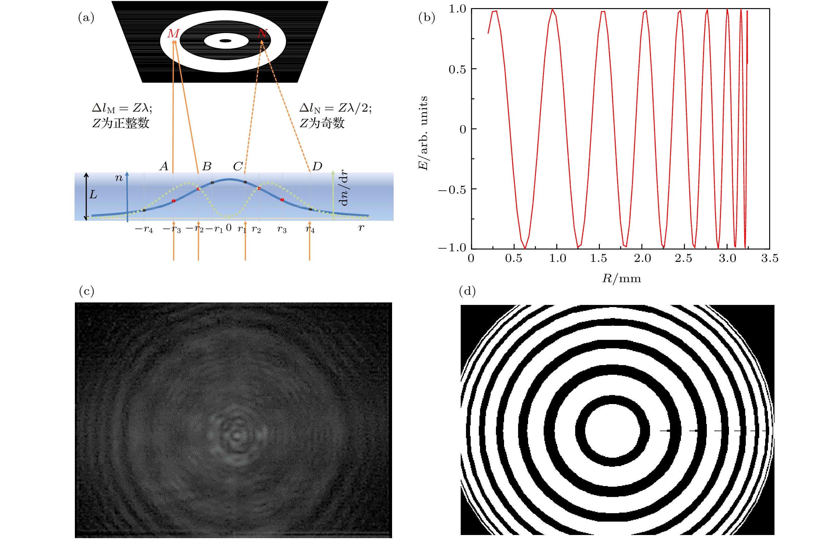 图 4 干涉环的形成机制 (a) 超快脉冲激光在实空间的光强分布导致了非线性折射率分布的差异, dn/dr相等的两个光束的出射方向相同, 但光程差不同; 当光程差是入射波长的整数倍时(如图中所示的A, B两束光到M点), 干涉相长, 由于透射光束关于光轴的圆对称性, 出现亮环; 是半整数倍时(如图中所示的C, D两束光到N点), 干涉相消, 出现暗环; (b) 同图1(d); 用n2为2.5 × 10⁻¹⁰ cm2/W时模拟得到的干涉图案, (c)为径向分布; (d)为记录平面里的干涉环
Figure4. Schematics of the formation mechanism of the interference rings. The intensity distribution of the ultrafast pulse laser in real space leads to the nonlinear refractive index distribution in the GaAs crystal. The two beams with same dn/dr are outgoing in the same direction. When the optical path difference between them is an integer multiple of the incident wavelength (e.g., the beams A and B which meet at point M, as shown in the left part of panel (a)), a bright ring appears due to instructive interference and the axial symmetry of the system. When it is a half-integer multiple of the incident wavelength (e.g., the beams C and D which meet at point N, as shown in the right part of panel (a)), a dark ring appears. (b) The same as Fig. 1(d). Simulation with n2 is 2.5 × 10⁻¹⁰ cm2/W: (c) Interference pattern along the radial direction; (d) interference pattern on the camera plane.
采用1 kHz的脉冲激光作为入射光源照射GaAs晶体时, 透镜前测得的入射激光功率为0.5 mW, 单个脉冲能量为0.5 μJ, 激光束径约为1 mm, 焦点处的光斑束径为14 μm, 对应的瞬态平均光强密度是8.1 GW/mm2. 在单路连续Z-扫描中, GaAs晶片在凸透镜焦点前后3 cm的范围内移动均可观测到干涉环, 由此判断出现干涉环所需的瞬态光强密度约为1 MW/mm2. 样品在一些典型位置时, 高速相机拍摄的干涉环如图1(b)—(d)所示. 这些干涉环都是多级的环形结构, 呈现显著的圆对称, 图1(b)、图1(c)和图1(d)是高速相机拍摄的干涉环, 样品与透镜焦点的距离分别是25 mm, 15 mm和10 mm (分别对应图1(a)左上方插图里的A, B和C三个位置). 当GaAs晶体片逐渐靠近透镜的焦点F时, 干涉环逐渐向外扩张, 从亮斑中心逐渐向外“吐”出更多圆环, 且随着入射光密度的增大, GaAs晶体片的非线性吸收增强, 透射光强变小, 高速相机采集的干涉环的图片亮度逐渐变暗. 反之, 当远离透镜焦点时, 干涉环向内收缩, 环慢慢湮灭, 环的个数减少, 但干涉环的总体亮度逐渐增强. 完整的实验录像见video-1 (
采用80 MHz的脉冲激光作为入射光源进行单路实验时, 对应的瞬态平均光强密度为0.5—5.7 MW/mm2. 在GaAs晶片逐渐靠近透镜焦点时, 普通CCD可以清楚地观测到从只有一个亮斑、没有干涉环到形成3圈干涉环的过程. 完整的实验录像见video-2 (
还利用这三种光源做了单路Z-扫描反射实验, 只能看到反射的亮斑, 没有观测到任何的干涉环结构, 说明表面没有发生任何形变.
挡住b路, 让a路激光照射GaAs晶片, 同样出现干涉环. 让两路激光同时照射, 也出现干涉环, 但是具体情况依赖于两束光的光程差. 利用图1(a)装置进行双路Z-扫描实验, 图2是单路、双路激光入射GaAs晶体的干涉环对比, 将样品放置在距离透镜焦点10 mm处, 设置两路光程差为2 cm, 调节两路入射功率均为0.2 mW, 高速相机拍摄的a路和b路脉冲激光单独入射到GaAs晶体产生的干涉环如图2(a)和图2(b)所示, 拍摄的a路和b路脉冲激光同时入射到GaAs晶体产生的干涉环如图2(c)所示. 然后, 调节两路入射功率分别为0.4 mW, 拍摄的a路脉冲激光单独入射到GaAs晶体产生的干涉环如图2(d)所示. 图2(a)、图2(b)和图2(c)的干涉环基本相同(图2(c)的亮度更大一些), 图2(d)的干涉环略多一些.
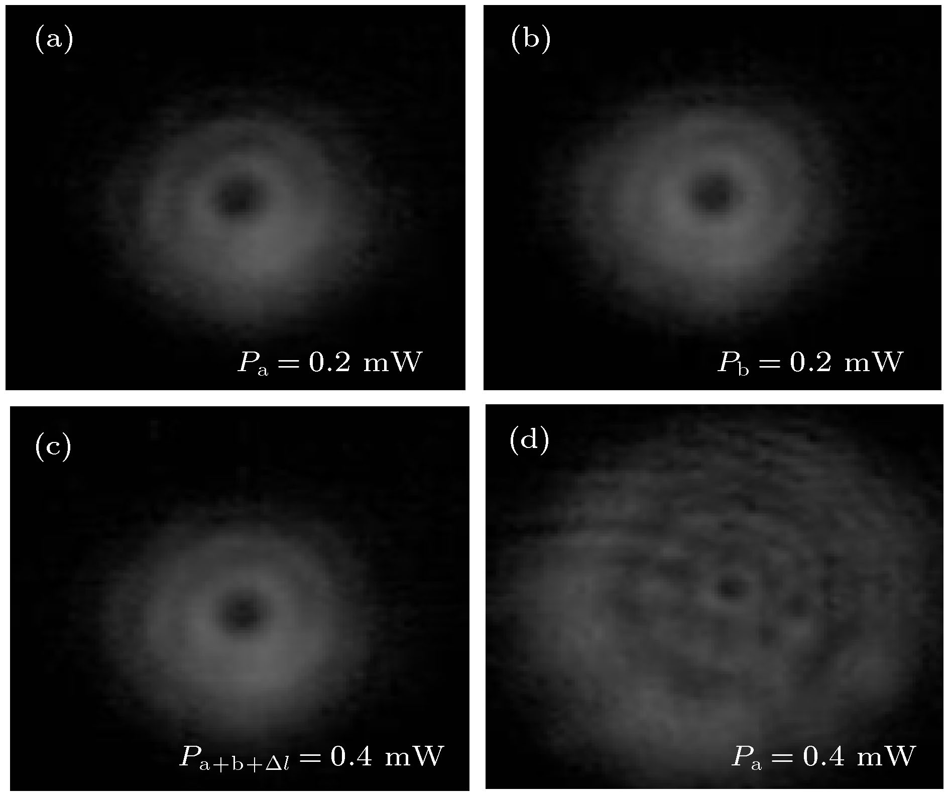 图 2 用单路或双路激光入射GaAs晶体时, 干涉环的对比(利用图1(a)双路实验装置, 调整a路与b路的光程差为Δl = 2 cm) (a), (b) 分别为入射功率为0.2 mW时, 高速相机拍摄的a路、b路单独入射到GaAs晶体形成的干涉环; (c) 高速相机拍摄的a路、b路同时入射时的干涉环; (d) 入射功率为0.4 mW时高速相机拍摄的a路单独照射时的干涉环
Figure2. Comparison of interference rings observed with single and/or dual lasers incident on GaAs crystal. Using the set-up shown in Fig. 1(a), the optical path difference between a and b is set to Δl = 2 cm. (a) The interference rings of beam a only, Pa = 0.2 mW; (b) the interference rings of beam b only with Pb = 0.2 mW; (c) the interference rings of beam a and b, Pa+b+Δl = 0.4 mW; (d) the interference rings of beam a only, Pa = 0.4 mW.
超快强光脉冲不同于连续激光, 高斯光束的透射率t''为

在双路系统实验中, 设置a路和b路光程差Δl = 2 cm, 相同功率的双路脉冲同时入射与a路或b路单路脉冲照射GaAs晶体的透射光强不同, 如图3所示. a和b两路脉冲分别以入射功率为0.2 mW和0.4 mW单独作用于样品, 透射光强随位置的变化趋势说明GaAs晶体在脉冲激光作用下有明显的非线性效应, 图中实线为最佳拟合曲线, Pa+Pb表示两单路的透射功率的直接加和, Pa+b+Δl表示a路与b路脉冲以67 ps的时间间隔同时作用于样品. 从图3可以直观地看出, 当入射功率相同时, 由于两路光程差的影响, 双路作用的非线性效应弱于单路作用的非线性效应.
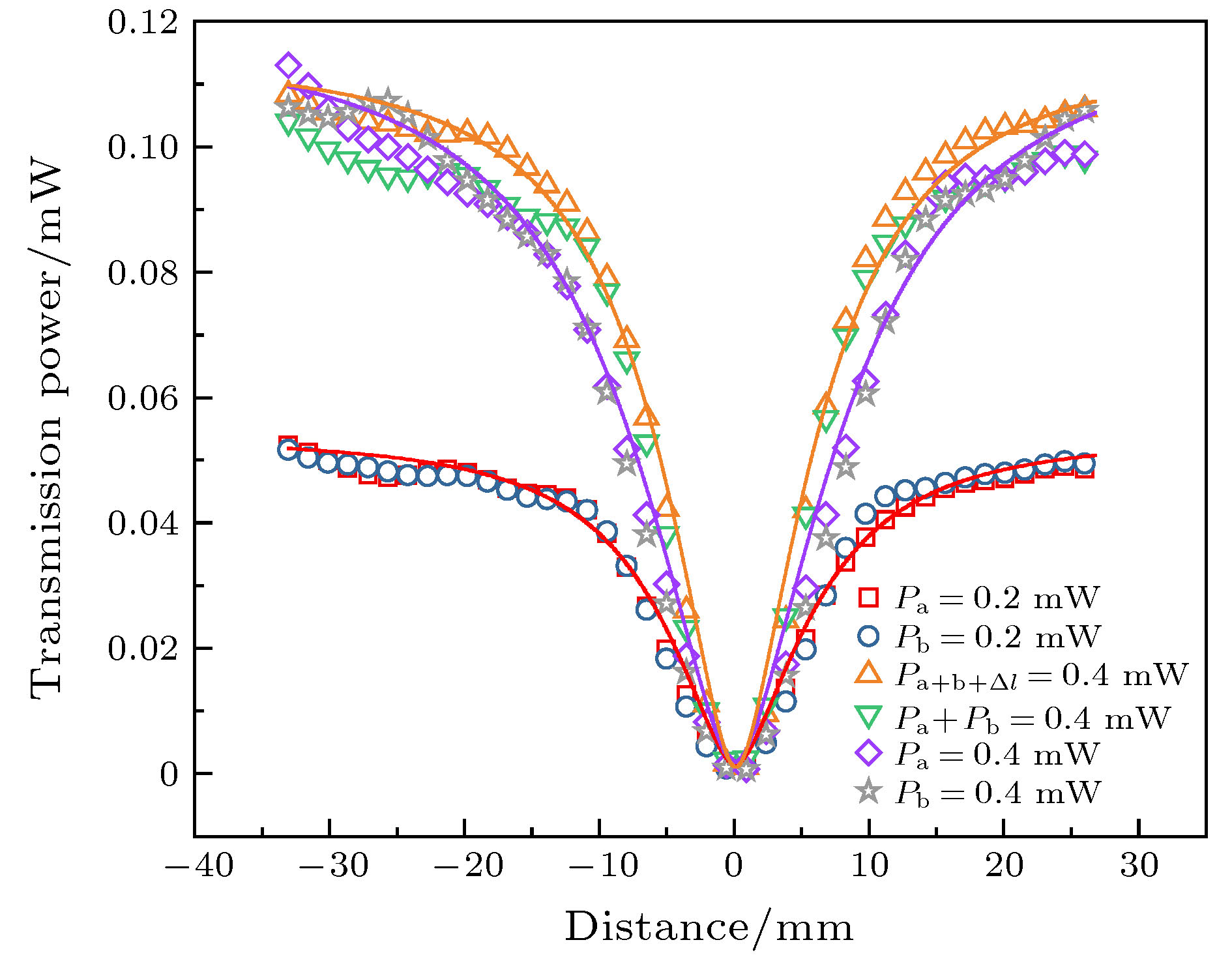 图 3 单路或双路激光入射GaAs晶体时的非线性透射功率, 其中, Pa = 0.2 mW, Pb = 0.2 mW, Pa = 0.4 mW, Pb = 0.4 mW四种不同符号分别为单路脉冲直接作用在GaAs的透射功率的实验结果; Pa+b+Δl的符号△为双路脉冲同时作用在GaAs的透射率变化, 其中Δl = 2 cm, 两路的入射功率相同, 光程差为2 cm, 总功率为0.4 mW; Pa+Pb的符号▽为Pa = 0.2 mW, Pb = 0.2 mW两路透射功率的直接加和; 实线对应于用(1)式拟合的结果
Figure3. Nonlinear transmission power of single and/or dual laser incident on GaAs crystal. Four symbols labeled with Pa = 0.2 mW, Pb = 0.2 mW, Pa = 0.4 mW, Pb = 0.4 mW are experimental results of the transmission power of single-channel pulse directly acting on GaAs. The solid lines are the best fits. The symbol △ labeled with Pa+b+Δl is the change of the transmission power with dual pulses simultaneously acting on GaAs. The incident power of two channels is the same with optical path difference Δl = 2 cm, and the total power is 0.4 mW. The symbol ▽ labeled with Pa+Pb is the sum of the transmission power of two beams Pa = 0.2 mW and Pb = 0.2 mW. Solid lines are fitting results with Eq. (1).
通过拟合单路Z-扫描的透射功率与位置之间的变化函数, 得到GaAs晶片的线性吸收系数


在双路Z-扫描实验中, 两路脉冲光除了光程的差别外, 其他参数都一致. 虽然激光在空气中会随着传播距离逐渐发散, 但是两束激光不会因为短距离的光程差有太大差别, 因此两路测得GaAs晶体的非线性曲线差别不大; 此条件下的两路光的共同作用如果等效于单独作用的直接加和, 就表示前一路脉冲对GaAs晶体的影响在下一路脉冲来之前已经消失, 干涉环的形成属于单个脉冲的作用, 形成时间短于两路的光程差.
我们认为干涉环源于脉冲激光在GaAs晶体中的非线性效应, 在改变样品位置的过程中, 透射光的强度有明显的变化. GaAs晶体的折射率n线性依赖于入射光强密度I, 即

