1.School of Physics and Technology, Center for Electron Microscopy, MOE Key Laboratory of Artificial Micro- and Nano-structures, and Institute for Advanced Studies, Wuhan University, Wuhan 430072, China 2.Suzhou Institute of Wuhan University, Suzhou 215123, China 3.Wuhan University Shenzhen Research Institute, Shenzhen 518057, China
Fund Project:Project supported by the National Natural Science Foundation of China (Grant Nos. 51871169, 51671148, 11674251, 51501132, 51601132), the Natural Science Foundation of Jiangsu Province, China (Grant No. BK20191187), the Fundamental Research Funds for the Central Universities, China (Grant No. 2042019kf0190), the Science and Technology Program of Shenzhen, China (Grant Nos. JCYJ20190808, 150407522), and the China Postdoctoral Science Foundation (Grant No. 2019M652685)
Received Date:04 June 2020
Accepted Date:18 June 2020
Available Online:30 September 2020
Published Online:05 October 2020
Abstract:Two-dimensional (2D) niobium silicon telluride (Nb2SiTe4) was recently proposed as a promising candidate in infrared detector, photoelectric conversion, polarized optical sensor and ferroelastic switching application due to its narrow bandgap, long-term air stability, high carrier mobility, etc. However, the in-plane strains and interfacial defects induced by the lattice misfits between functional layers are harmful to 2D heterojunction nanodevice performance, making the crystal-lattice regulation and strain engineering necessary to achieve lattice matching and strain-controllable interface. Here, using first-principles calculations and elemental substitutions, i.e., replacing cations (anions) with elements in the same group of periodic table, we identify three new and stable single-layer A2BX4 analogues (Nb2SiSe4, Nb2SnTe4 and Ta2GeTe4) as appealing candidates in manipulating the lattice parameters of Nb2SiTe4. The controllable lattice parameters are 6.04 ? ≤ a ≤ 6.81 ? and 7.74 ? ≤ b ≤ 8.15 ?. Among them, Ta2GeTe4 exhibits similar lattice parameters to Nb2SiTe4 but smaller bandgap, yielding better response in far-infrared region. Strain engineering shows that the external biaxial tensile stress narrows the bandgaps of A2BX4 due to the downshifting in energy of conduction band minimum (CBM). External biaxial compressive stress induces valance band maximum (VBM) orbital inversion for Nb2SiTe4, Nb2GeTe4 and Ta2GeTe4, which pushes up VBM and discontinues the trend of corresponding bandgap increase. In this case, the bandgap change depends on the competition between energy upshifts of both CBM and VBM. In the Nb2SiSe4 and Nb2SnTe4 cases, the d-p antibonding coupling in valance band is so strong that no valance band inversion appears while the bandgap increases by ~0.3 eV under ?5% compressive strain. Regarding Nb2SiTe4, Nb2GeTe4 and Ta2GeTe4, their bandgaps can hardly change under ?5% compressive strain, indicating that the energy upshift in VBM equals that in CBM. Such a valance band inversion is attributed to Te outmost p orbital overlapping, which introduces more dispersive VBM and smaller effective mass of hole. Our findings suggest that Nb2SiTe4 can be alloyed with Nb2SiSe4, Nb2SnTe4 and Ta2GeTe4 to achieve controllable device lattice matching while maintaining its superior properties at the same time. The use of external biaxial compressive stress can promote the hole diffusion and improve the device performance. Keywords:Nb2SiTe4/ elemental substitution/ strain engineering/ first-principles calculations
我们计算了上述5种单层A2BX4化合物的光学性质. 图4(a)沿x方向, 图4(b)沿y方向. 阴影部分为AM1.5G太阳辐射光谱. 可以看出此系列材料在红外到紫外光区间内均具有较强的光吸收特性(光吸收系数在105 cm–1量级), 可以应用于红外光探测和光伏器件之中. 此外, A2BX4化合物沿x方向的光吸收较y方向更强, 具有明显的光学各向异性, 表明其在偏振光探测方面有潜在应用. 图 4 计算的5种A2BX4光吸收谱 (a) 沿x方向; (b) 沿y方向 Figure4. Calculated optical absorption coefficients for five A2BX4 compounds along (a) x direction and (b) y directions.
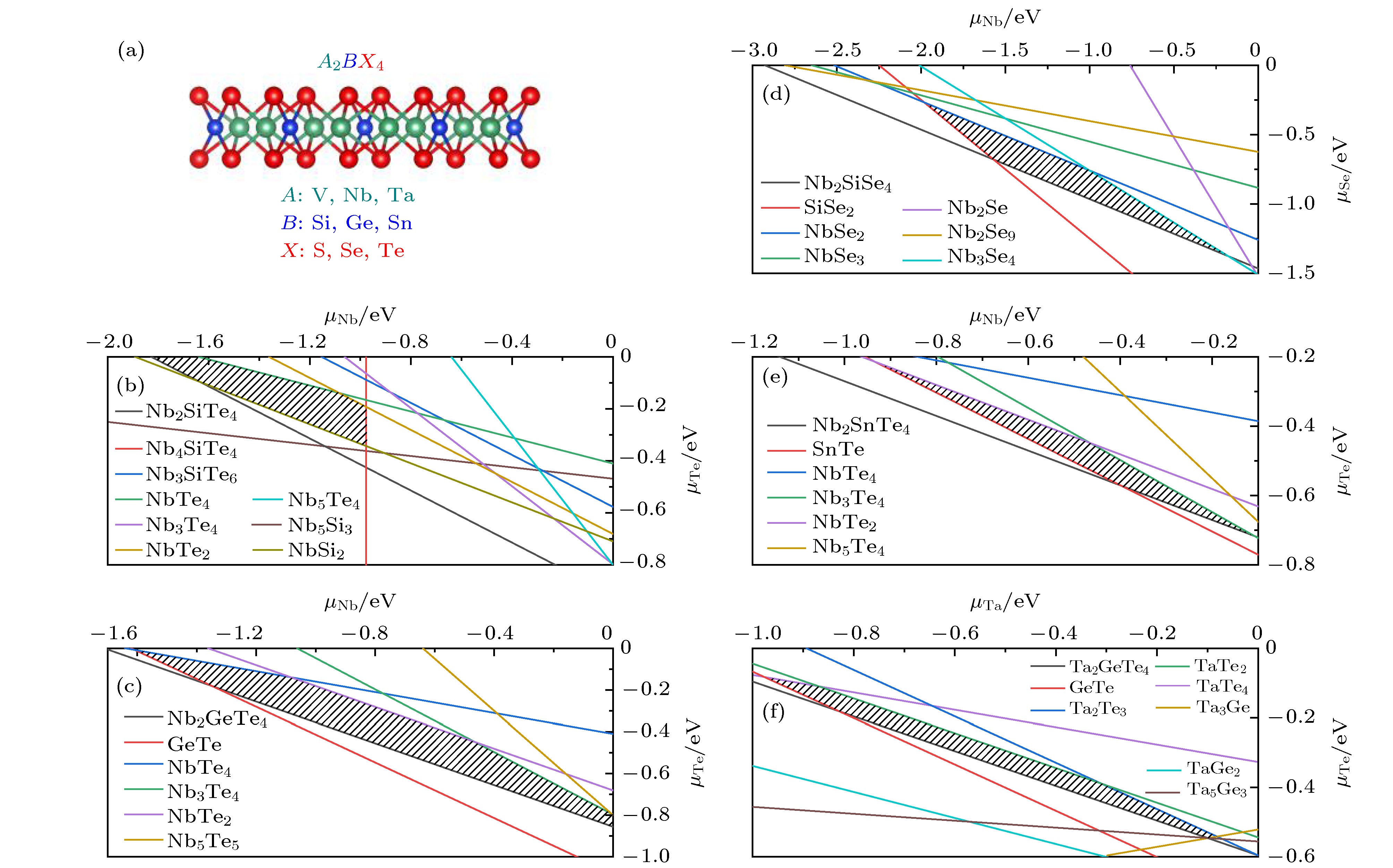 图 1 (a) 二维A2BX4化合物的晶体结构图; (b)—(f) 筛选出的5种稳定A2BX4化合物的化学势能窗口图, 分别对应Nb2SiTe4, Nb2GeTe4, Nb2SiSe4, Nb2SnTe4和Ta2GeTe4.
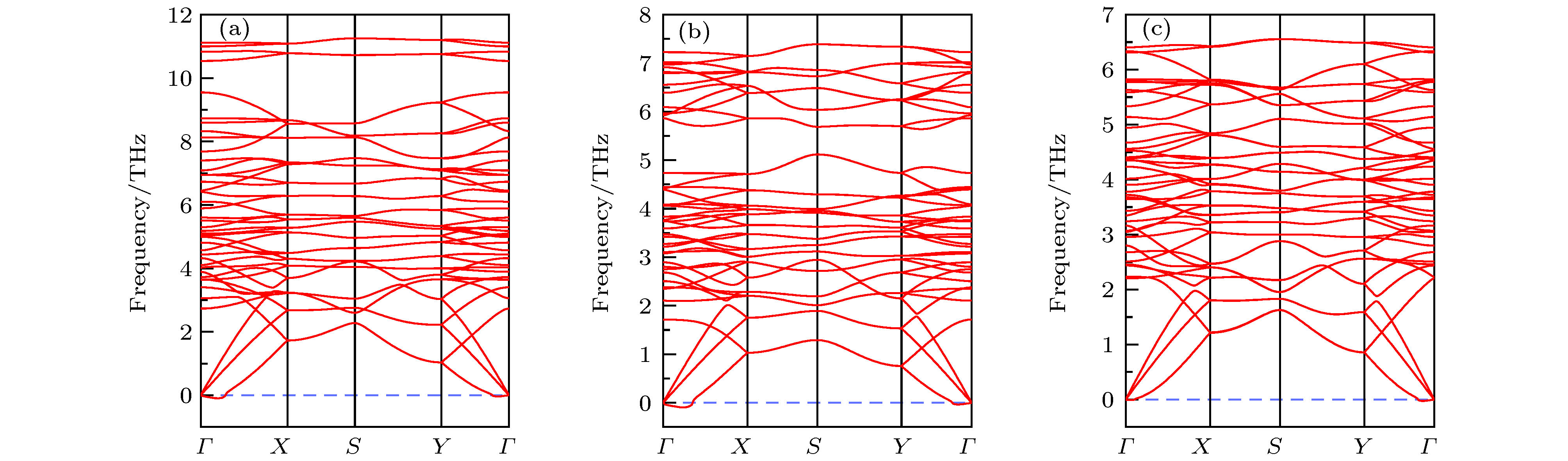 图 2 0 K下基于PBE计算的声子谱 (a) Nb2SiSe4; (b) Nb2SnTe4; (c) Ta2GeTe4
 图 3 HSE06计算的能带结构 (a) Nb2SiSe4; (b) Nb2SiTe4; (c) Nb2GeTe4; (d) Nb2SnTe4; (e) Ta2GeTe4. 其中蓝线(绿线)代表Nb2SiTe4的VBM(CBM)位置, 数字表示相比Nb2SiTe4 VBM(CBM)的移动
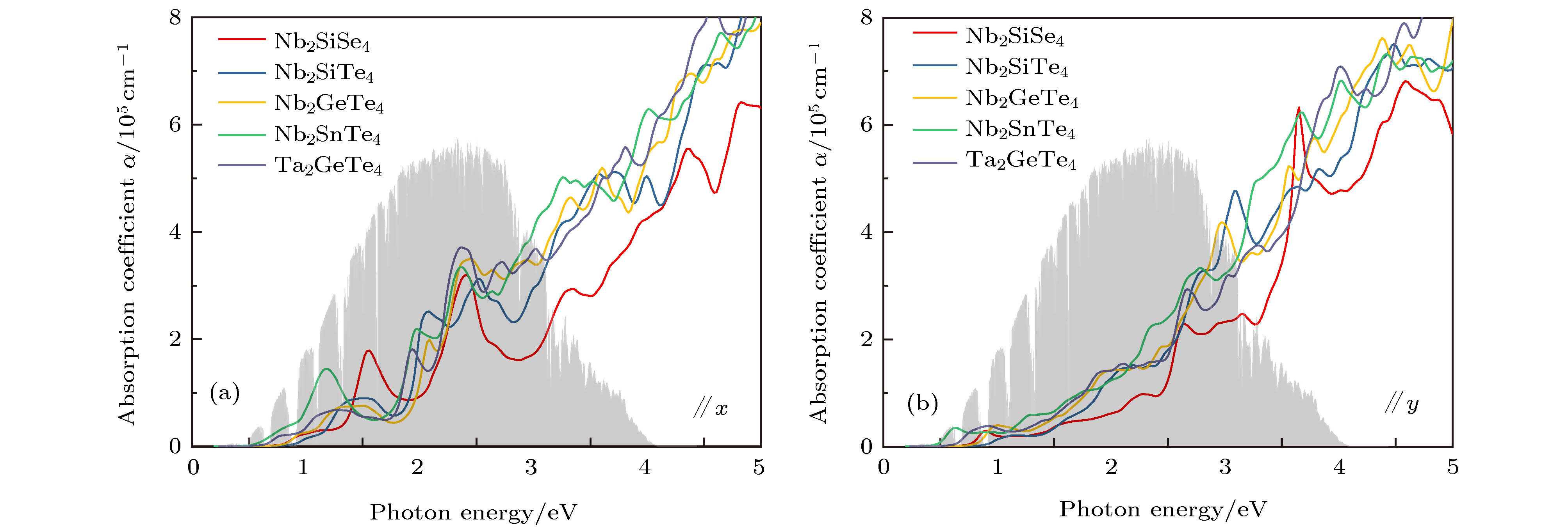 图 4 计算的5种A2BX4光吸收谱 (a) 沿x方向; (b) 沿y方向
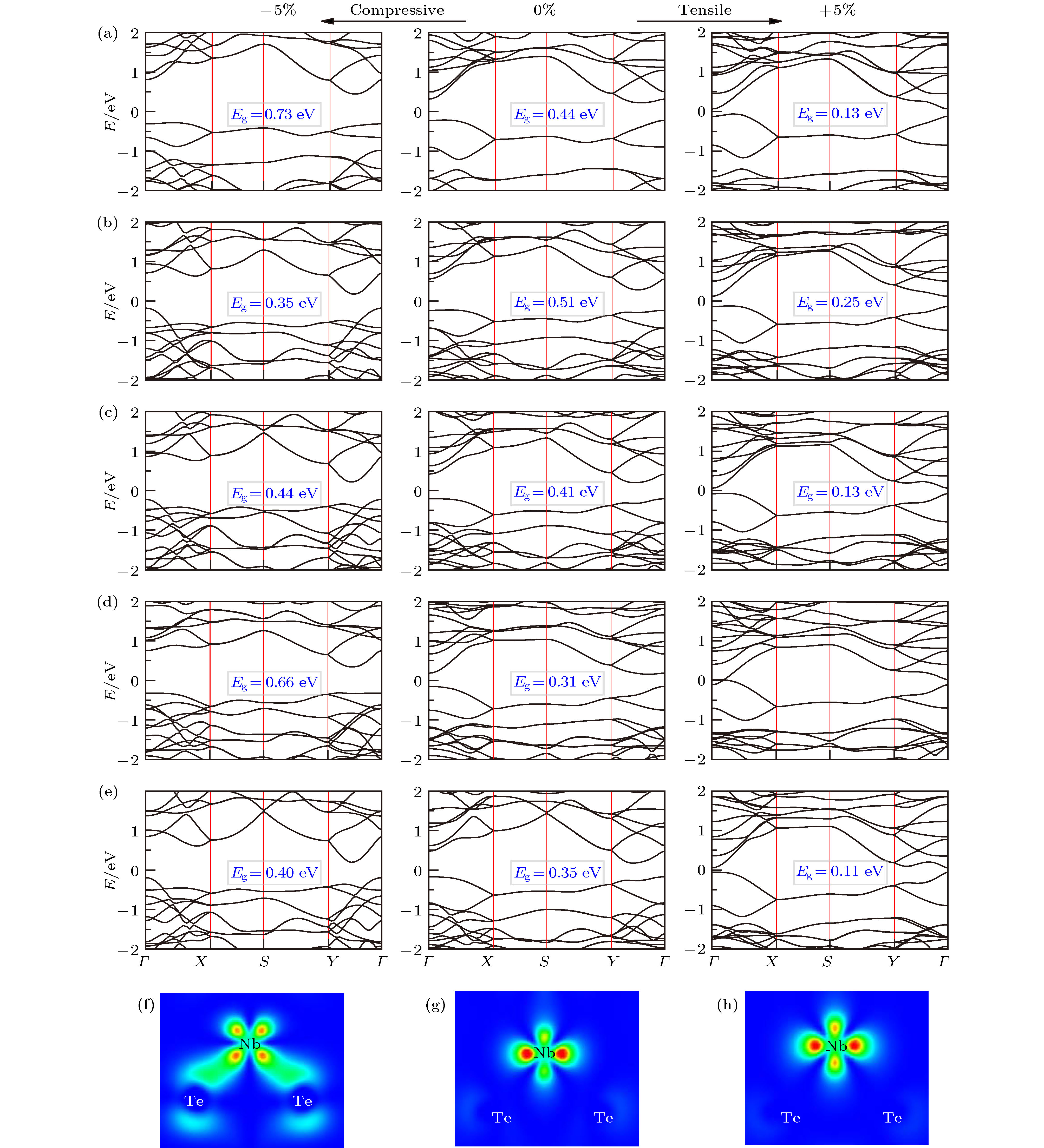 图 5 PBE计算的外加 ± 5%应力时A2BX4的能带结构图 (a) Nb2SiSe4; (b) Nb2SiTe4; (c) Nb2GeTe4; (d) Nb2SnTe4; (e) Ta2GeTe4; (f), (g), (h)为对应外应力下Nb2SiTe4 VBM的电荷密度图