Science and Technology on High Power Microwave Laboratory, Institute of Applied Electronics, China Academy of Engineering Physics, Mianyang 621900, China
Fund Project:Project supported by the Science Foundation of the High Power Microwave Laboratory, China (Grant No. 6142605180203)
Received Date:28 June 2020
Accepted Date:07 July 2020
Available Online:02 November 2020
Published Online:05 November 2020
Abstract:The relativistic klystron amplifier (RKA) is a very important kind of high power microwave device, which has the advantages of high power, high efficiency, stable output phase and amplitude. The development of multi-injection RKA toward engineering and practical application needs to further improve operating frequency and output power of klystron amplifier, while the RKA of conventional circular waveguide drift tubes is restricted by the physical factors such as geometric size, space charge force and high-voltage breakdown. The multi-beam RKA based on the technology of multiple electron beams can work at low voltage and guiding magnetic field, and can also possess high electron beam current and diversion coefficient. The physical limitation of conventional structure RKA is overcome, and the working frequency and the output power are improved. In the experiment, the X-band GW level power of microwave is obtained. The multi-beam RKA needs to further improve its working frequency and working life. In the experiment, the power conversion efficiency of multi-beam RKA is about 35%, and most of the remaining electron energy will accumulate on the collection pole at the end. If the heat dissipation of the collector is not designed appropriately, the collection will be seriously ablated when working at high heavy frequency. Thus a large quantity of plasma and secondary electrons are generated, which affects the stability of the device. To solve the problem of electron reflux bombarding the output cavity after electron beam exchanging energy in the gap of output cavity, the reflux process of relativistic electron beam in the device is analyzed in this paper. On this basis, a coaxial extraction structure with four-gap extension interaction is designed to avoid electron reflux and reduce the gap electric field, thus improving the working life of the device. At the same time, in order to solve the problem that the conventional water cooling channel can affect the output microwave mode in a high-frequency over-mode device, a mode transformation structure of coaxial TEM mode-fan-shaped TE10 mode-coaxial TEM mode-circular waveguide TM01 mode is designed. The mode conversion efficiency is greater than 99.9%, and the influence of collecting polar water cooling channel on the output microwave mode is avoided. The stable operation of multi-beam RKA in the X-band with a repetition rate of 45 Hz is realized experimentally, while the output power is over 1 GW and the microwave pulse width is over 100 ns. At present, the multi-beam RKA runs about 10000 times in total, and the output microwave parameters do not decrease significantly. Keywords:relativistic klystron amplifier/ X-band/ long pulse/ high repetition rate
式中, U0为二极管电压, γ0为相对论因子, me为电子质量, c为真空中的光速. 设定电子束的电压U0为700 kV, 电子束离器件中心的距离rb为35 mm, 同轴结构内半径ri为30 mm, 同轴结构外半径rw为40 mm. 在不同的电子束电流I0情况下, 由(1)式和(2)式结合器件尺寸, 图1所示同轴输入腔、中间腔1、中间腔2和输出腔的内外半径分别约为46 mm/25.5 mm, 45 mm/26 mm, 45 mm/26 mm, 45 mm/26 mm (输出腔最后一间隙径向尺寸为49 mm/26 mm), 可得到直流电子束在器件同轴结构中传输时, 其势能与总能量的比值Ep/E0的变化如图3所示. 图 3 直流电子束在器件中传输时Ep/E0的变化 Figure3. Changes of Ep/E0 when the electron beam is transmitted in the device.
3.输出腔结构优化设计由于器件中电场强度最大位置在输出腔间隙处, 要实现器件稳定工作, 输出腔间隙电场强度需要低于击穿阈值, 以避免射频击穿导致脉冲缩短和输出腔结构表面烧蚀. 为了抑制电子返流, 同轴输出腔内外边界与电子束的径向距离需要减小, 以减小群聚电子束在输出腔间隙处的势阱. 提高器件的过模比(器件漂移管直径与工作波长λ的比值, 本文中多注速调管按照2rw/λ计算), 有利于降低间隙的电场强度和降低电子束的空间电荷效应, 因此将X波段多注RKA的过模比由原先的1.3提高为约2.5. 同时对输出腔结构进行改进设计, 设计了四间隙扩展互作用输出腔结构以降低间隙电场强度. 输出结构采用π模工作模式, 相邻间隙的轴向电场方向相反. 设计四间隙π模工作输出腔的电子负载电导为负值, 使得工作模式易于被电子束激励, 同时每个间隙长度Lgap满足βeLgap < π, 其中βe = 2πf/v0, f为工作频率. 电子束通过输出腔间隙时能够产生较好的换能, 以提高功率转换效率. 并且多间隙过模结构有利于减小输出腔内外边界与电子束的径向距离(相比于常规结构可减小约10%), 减小电子束在输出腔间隙处产生的势阱, 以避免电子返流. 粒子模拟仿真电子束电压为700 kV, 束流为8.5 kA, 轴向引导磁感应强度为0.8 T, 在该参数下早期设计的双间隙输出腔输出微波功率约为2 GW, 转换效率约为34%, 双间隙输出腔结构最大电场强度约为1.3 MV/cm, 大于击穿阈值. 改进设计后粒子仿真四间隙扩展互作用输出腔输出微波功率约为2.4 GW, 转换效率为40%. 此时输出间隙结构的轴向电场Ez分布如图4(b)所示, 间隙最大电场强度小于700 kV/cm, 低于X波段的经验击穿阈值800 kV/cm. 图 4 输出微波与间隙电场分布 (a)输出微波波形; (b)输出腔电场分布 Figure4. Distribution of output microwave and gap electric field: (a) Output microwave waveform; (b) electric field distribution of the output cavity.
粒子模拟仿真改进设计前后的电子束相空间图和电子束电流随轴向传输距离的变化如图5和图6所示. 图 5 改进设计前后电子束相空间图 (a)改进设计前; (b)改进设计后 Figure5. Electron beam phase space diagram: (a) Before the improved design; (b) improved design.
图 6 改进设计前后电子束电流随轴向传输距离的变化 (a)改进设计前; (b)改进设计后 Figure6. Changes of electron beam current with axial transmission distance: (a) Before the improved design; (b) improved design.
返流电子为图5中轴向动量小于零的电子(图中蓝色线下方的电子). 由图5和图6可知, 改进设计后粒子仿真结果显示, 抑制了电子束在输出腔间隙返流和束流损失, 有利于提高器件的工作稳定性和工作寿命. 4.水冷却收集极的优化设计实际的器件实验中, 电子束功率约为6 GW, 群聚电子束通过输出腔换能后, 仍有约4 GW的剩余功率, 电子束脉宽约为150 ns, 在重频45 Hz工作条件下, 收集极处电子束的平均功率约为27 kW. 高重频工作条件下, 电子束平均功率较大, 为了增大器件持续工作时间, 需要及时将热量导出, 应采用具有外部水冷却结构的收集极[18,19]. 同时电子束峰值功率很高, 需要结合磁场位形进行设计使电子束在收集极处散开, 增大电子束轰击收集极面积, 避免过度烧蚀产生大量等离子体. X波段相对论速调管微波输出为轴向提取结构, 微波通道为过模结构以保证功率容量, 收集极在微波通道内部, 而水冷却通道尺寸较大, 器件工作在较高频段时, 引入该通道会产生较大的微波反射, 并导致输出微波模式产生变化, 因此对水冷却通道结构进行改进设计. 设计了同轴TEM模-扇形TE10模-同轴TEM模-圆波导TM01模的模式变换结构. 扇形波导的数目为12个, 以保证微波在扇形波导中的传输模式为基模TE10模, 相邻两个扇形波导之间最大的间隙角度θ1 = 8°, 对应间隙距离约为7 mm, 相应间隙的长度L1 = 12 mm, 可以提供水路传输的通道(设计水路通道为直径5 mm). 模式变换结构的电场分布与微波传输参数如图7和图8所示. 图 7 模式变换结构的电场分布 (a)纵向剖面; (b)横向剖面 Figure7. Electric field distribution of the mode transform structure: (a) Lengthwise section; (b) transverse section.
图 8 模式变换结构的S参数曲线 Figure8. The S parameter curve of mode transformation structure.
图7(a)为模式变换器纵向剖面结构与电场分布图, 图7(b)为扇形波导处的横向剖面结构与电场分布图. 由图8可知在频率9.35—9.45 GHz范围内, 输出微波的模式转换效率大于99.9%. 仿真计算中设定微波馈入端口的功率为0.5 W, 模式变换结构中最大电场强度为627 V/m, 计算得到当输出微波功率为3 GW时, 对应最大电场强度约为486 kV/cm, 低于击穿阈值, 设计的模式变换结构具有较高的功率容量. 5.重频长脉冲实验研究在长脉冲加速器平台开展X波段多注RKA器件高重频实验研究, 器件实验示意图如图1所示. 收集极设计了水冷却散热结构, 并且结合实际磁场位形对收集极的位置进行优化设计, 收集极处于磁场开始变弱的边缘位置, 换能后的电子束在收集极处散开[20], 尽量增大电子束轰击收集极的面积, 以避免高重频工作时收集极烧蚀. 重频45 Hz工作时, 加速器产生电子束电压与电流波形如图9所示. 图 9 重频45 Hz电子束重叠波形 Figure9. Overlapping waveform of electron beam at 45 Hz.

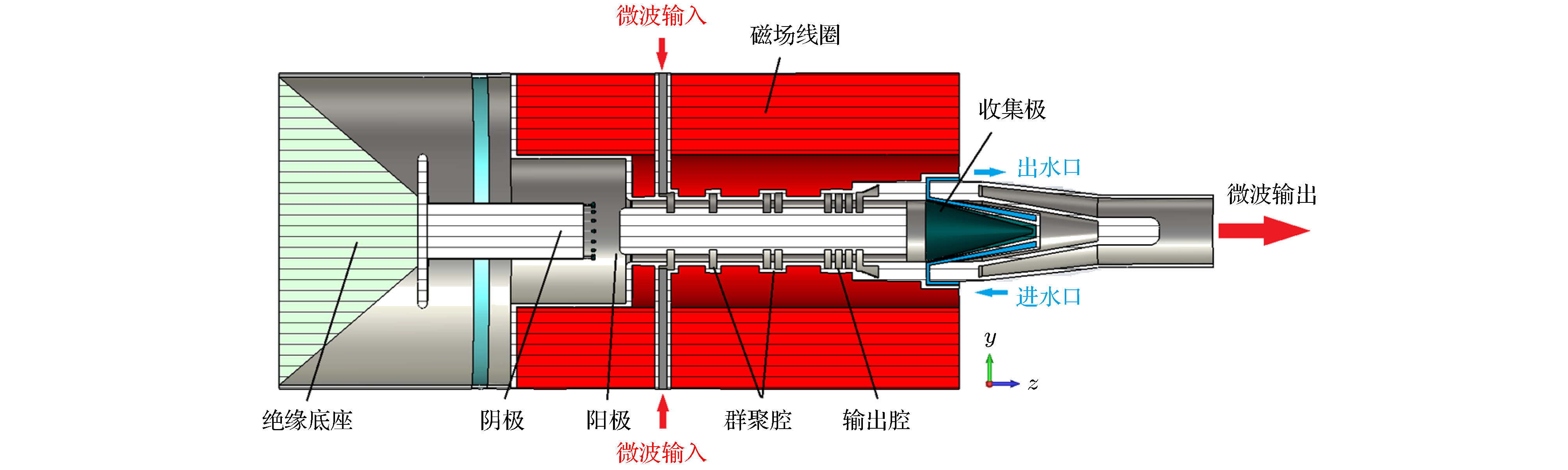 图 1 X波段多注RKA结构示意图
 图 2 强流电子束在同轴结构中传输
 图 3 直流电子束在器件中传输时Ep/E0的变化
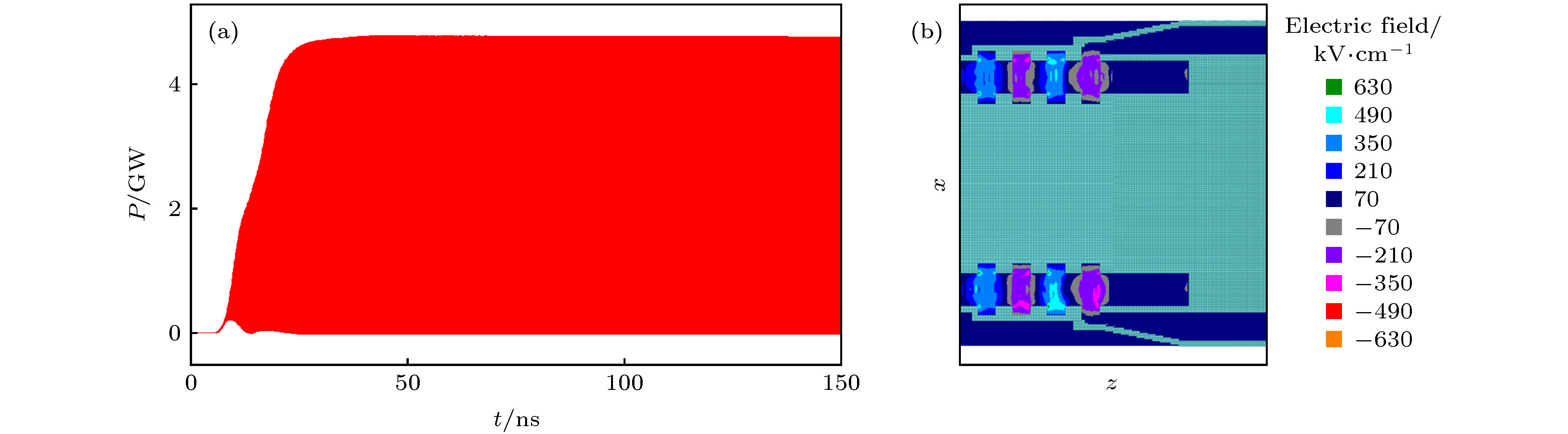 图 4 输出微波与间隙电场分布 (a)输出微波波形; (b)输出腔电场分布
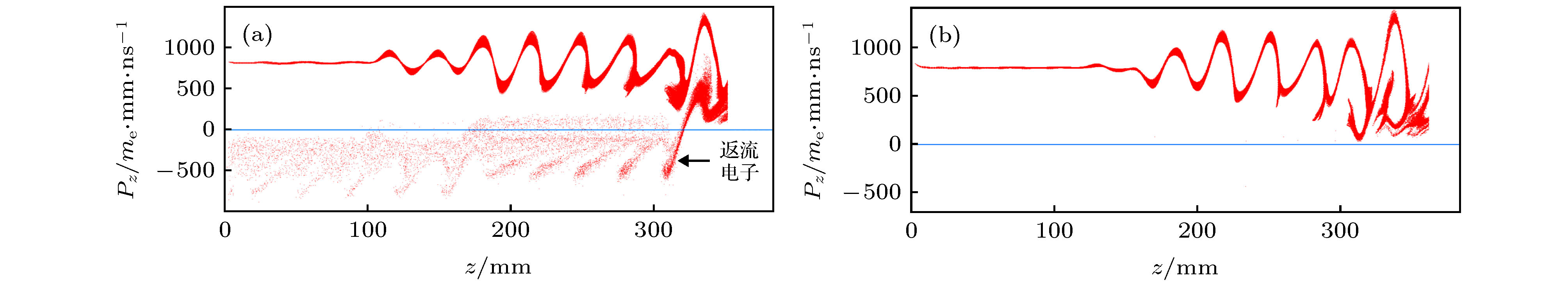 图 5 改进设计前后电子束相空间图 (a)改进设计前; (b)改进设计后
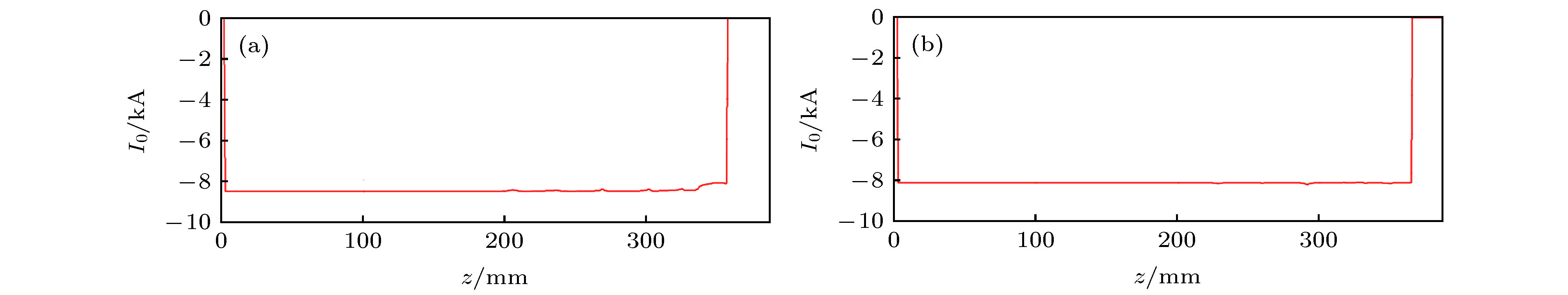 图 6 改进设计前后电子束电流随轴向传输距离的变化 (a)改进设计前; (b)改进设计后
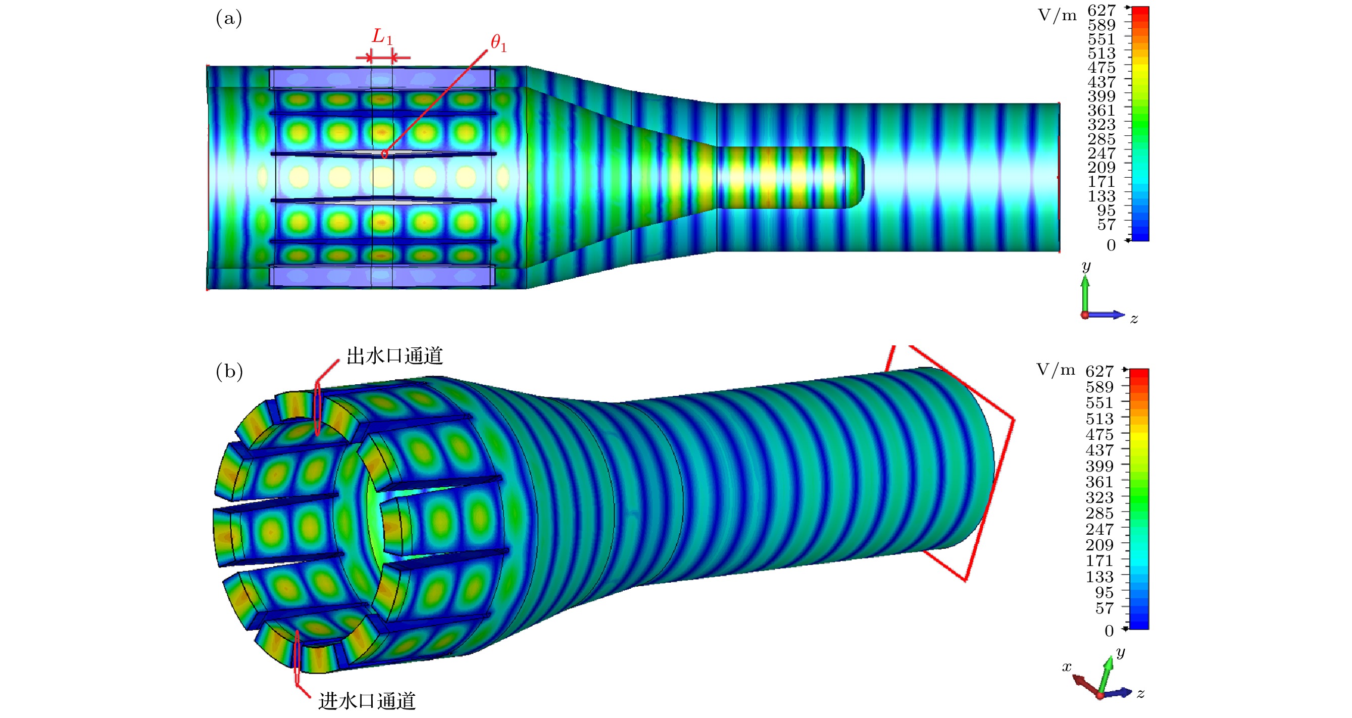 图 7 模式变换结构的电场分布 (a)纵向剖面; (b)横向剖面
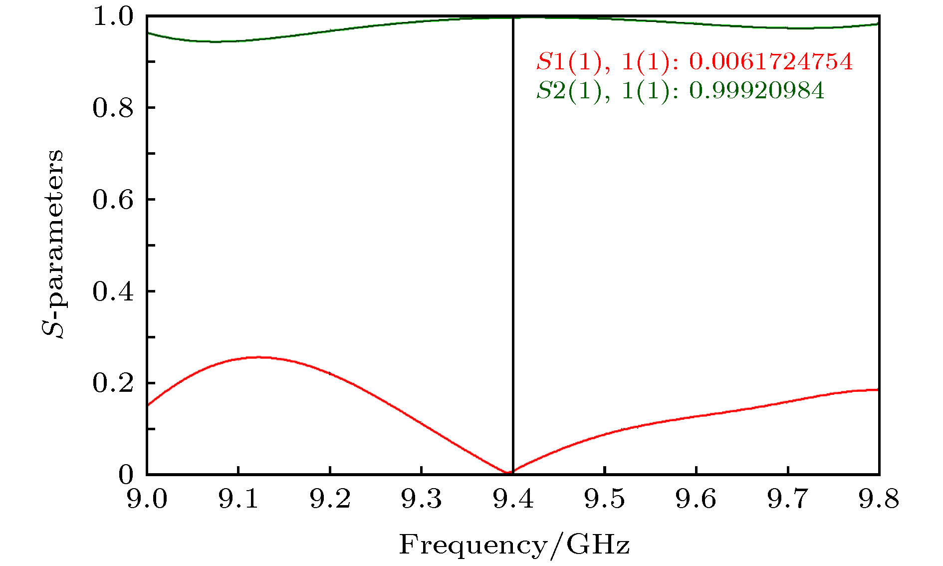 图 8 模式变换结构的S参数曲线
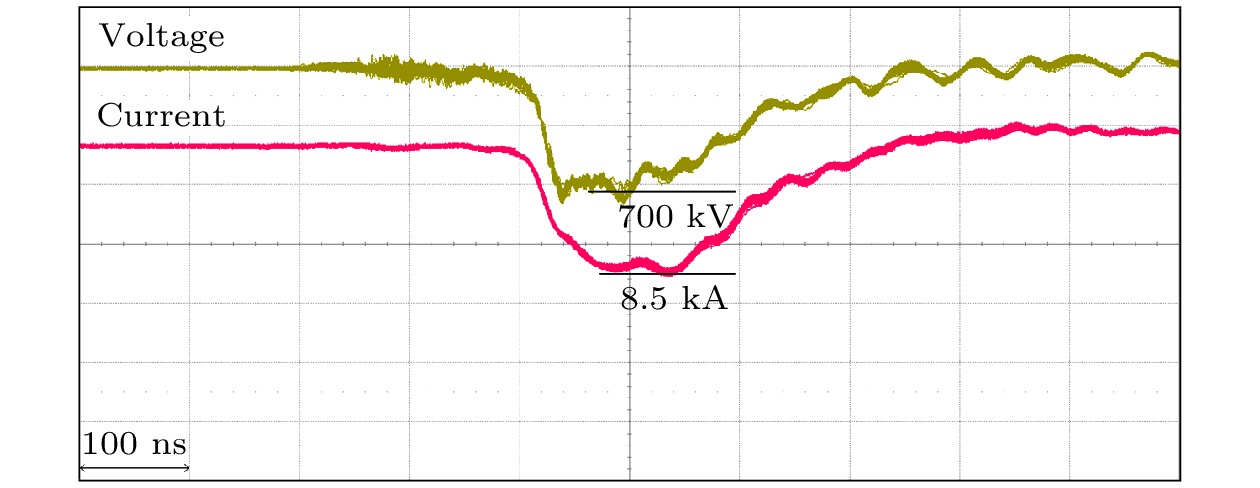 图 9 重频45 Hz电子束重叠波形
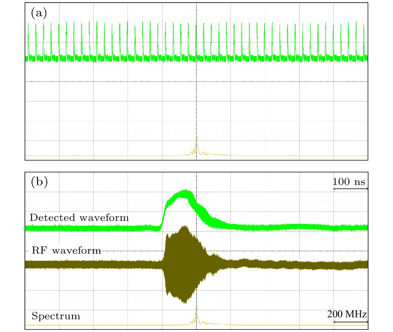 图 10 重频45 Hz微波序列与重叠波形 (a) 序列波形; (b) 重叠波形