全文HTML
--> --> -->


基于样品和探测器之间的距离(L), 可以将物质周围的电磁场区域分为三种类型[3]: 远场(


 图 1 近场光学成像原理图 (a)近场成像和远场成像的比较: 远场光学中物体的点扩散函数由传统衍射极限决定, 而近场光学中物体的点扩散函数由探针尺寸决定; (b)近场光学突破衍射极限的不确定原理解释
Figure1. Schematic of near-field optics. (a) Comparison between far-field and near-field optics. The point spread function in far-field optics is determined by the diffraction limit, while the spatial resolution in near-field optics is determined by the size of probe.(b) Explanation of breaking the diffraction limit in near-field optics based on uncertainty principle.


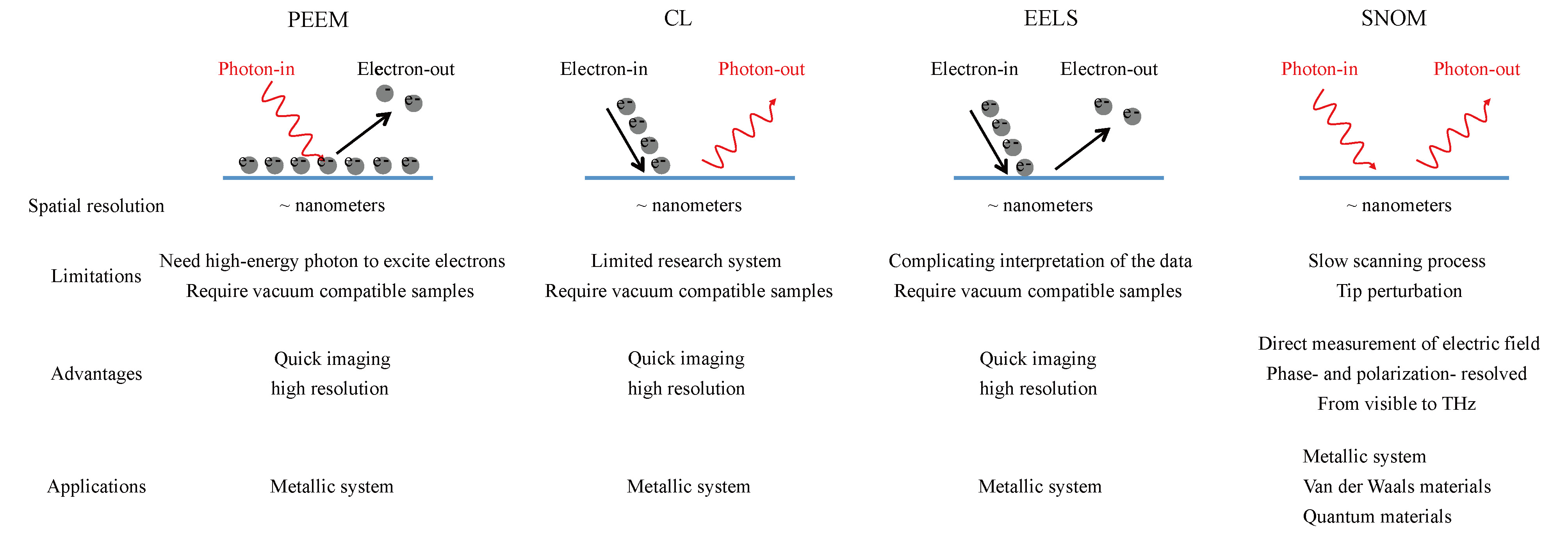 图 2 光发射电子显微镜(PEEM)、阴极荧光光谱(CL)、电子能量损失谱(EELS)、扫描式近场光学显微镜(SNOM)等不同纳米级成像技术之间的对比
Figure2. Comparison of four classical sub-wavelength approaches, including photon emission electron microscopy (PEEM), cathode-luminescence spectroscopy (CL), electron energy loss spectroscopy (EELS), and scanning near-field optical microscopy (SNOM).
本文主要介绍通过近场光学手段揭示二维极化激元学中的重要进展和实验结果. 首先, 给出近场光学概述及其成像的基本原理; 其次, 介绍二维极化激元学中近场研究进展的几个重要方向, 包括等离极化激元、声子极化激元、激子极化激元和杂化型极化激元; 最后, 介绍近场光学面临的挑战和今后可能的发展方向.
2.1.探针位置
近场光学成像中, 必须保证探针与样品之间的距离(


2
2.2.远场背景扣除
如何从远场散射背景中得到纯净的近场光学信号是近场成像必须考虑的问题[33,34]. 基于背景扣除的不同原理, 可以将SNOM分为孔径型SNOM[35,36]和散射型SNOM[37-39]两类. 如图3(a)所示, 孔径型SNOM将入射激光导入光纤, 再逼近至样品表面近场区域. 为了消除远场背景, 必须保证光纤直径(D)为纳米量级, 即光纤末端只收集纳米量级的局域电磁场信号. 故孔径型SNOM的空间分辨率取决于光纤直径的具体数值, 当然, 直径大小也决定着入射光在光纤末端的透射效率. 随着光纤直径的增大, 透射效率也在增大, 但分辨率却在降低. 例如, 当直径为100 nm时透射效率约为10–4, 而直径为50 nm时透射效率仅为10–5. 也就是说, 要选取一个合适的光纤直径, 既可以保证足够大的透射效率(信噪比), 又能尽量提高成像的空间分辨率. 目前孔径型SNOM能达到的最佳分辨率约为50 nm. 尽管在光纤上粘附金属纳米线可以进一步提高这一分辨率(图3(a)右), 但孔径型SNOM的应用依然很受限制. 这是因为其针尖制备非常复杂, 并且不可避免地存在光泄露问题. 而散射型SNOM在有效克服这些问题的同时还获得了10 nm左右的超高分辨率. 在散射型SNOM中需要将入射激光聚焦在探针尖端, 通常有两种方式: 间接型[40,41](图3(b)左)和直接型[19](图3(b)右). 间接型需要在针尖悬臂上刻蚀周期性光栅结构, 入射光激发等离激元, 并沿着光滑的探针表面传播, 最后在探针尖端聚焦, 产生纳米级局域电磁场, 又称“热点 (hot-spot)”. 这一电磁场为探测样品局域光学性质提供了纳米级光源. 与孔径型SNOM类似, 纳米级聚焦可以有效避免来自针尖悬臂和样品表面的散射背景信号, 且其实验中测量得到的光学对比度物理模型简单易懂. 然而, 间接型聚焦方式还存在很多问题: 首先, 探针悬臂上的周期性光栅结构制备复杂, 且必须精确计算光栅到探针尖端的距离; 其次, 无法得到物质近场相位信息; 最后, 等离激元的耦合效率仅为0.1%左右, 导致探针尖端局域电磁场强度很小, 无法有效激发二维材料中极化激元.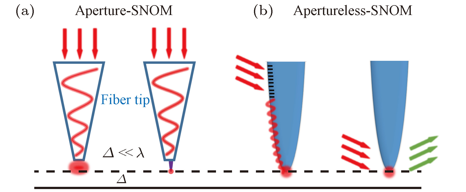 图 3 SNOM实验原理 (a) 孔径型SNOM照射原理; (b) 散射型SNOM照射原理
Figure3. Experimental scheme of SNOM: (a) The illumination scheme of a-SNOM; (b) the illumination scheme of s-SNOM.
为了克服这些瓶颈, Ocelic等[42]发展了直接聚焦(图3(b)右), 获得了更强的局域电磁场, 为二维极化激元学打开了一扇新的大门. 在直接聚焦中, 最核心的问题是如何去除来自探针悬臂和样品表面很强的散射背景信号. 探针散射的总电场强度(


2
2.3.探针材料和光偏振状态
在近场光学测量中需要注意两个细节, 即探针材料和光偏振状态. 因为散射型SNOM是一种扰动式成像手段, 必须要考虑针尖与样品之间近场相互作用对本征近场信号的影响[47]. 尽管金属和介质针尖都可以补偿极化激元和自由空间光之间的动量差, 但它们对近场成像的影响很不一样. 如图4(a)所示, 实验中[47]金属纳米结构的近场光学分布与所使用的针尖非常相关: 当使用碳纳米管针尖时(图4(a)左), 可以观察到金纳米圆盘周围电场的偶极子分布, 而金属针尖则对偶极子分布产生强烈扰动, 最终导致了近场强度的非对称分布. 这是因为当金属针尖的极化度近似于甚至强于金纳米盘偶极子本身的极化度时, 针尖和样品之间的强耦合就成为近场光学图像的决定性因素. 也就是说相比于介质针尖, 金属针尖会对本征近场光学分布产生更强的扰动. 另外一个不同是金属针尖会提供更大的局域场增强效应. 图4(b)展示了不同针尖与衬底间隙之间电场强度的数值模拟结果, 其中入射光偏振平行于针尖长轴方向. 可以看出, 金针尖产生了10倍于硅针尖的局域场强度, 这对二维极化激元学至关重要. 在近场扫描过程中, 金针尖往往同时扮演着激发源和探测源的双重角色, 而硅针尖仅为探测源. 所以选择针尖材料时, 必须在小的扰动(介质针尖)和增强的近场信号(金属针尖)之间权衡. 一般来讲, 硅针尖更多用于金属结构近场光学分布的测量, 这是因为金属的本征近场信号比较强. 而金属针尖则更多用于二维材料极化激元的探测以及光谱的测量.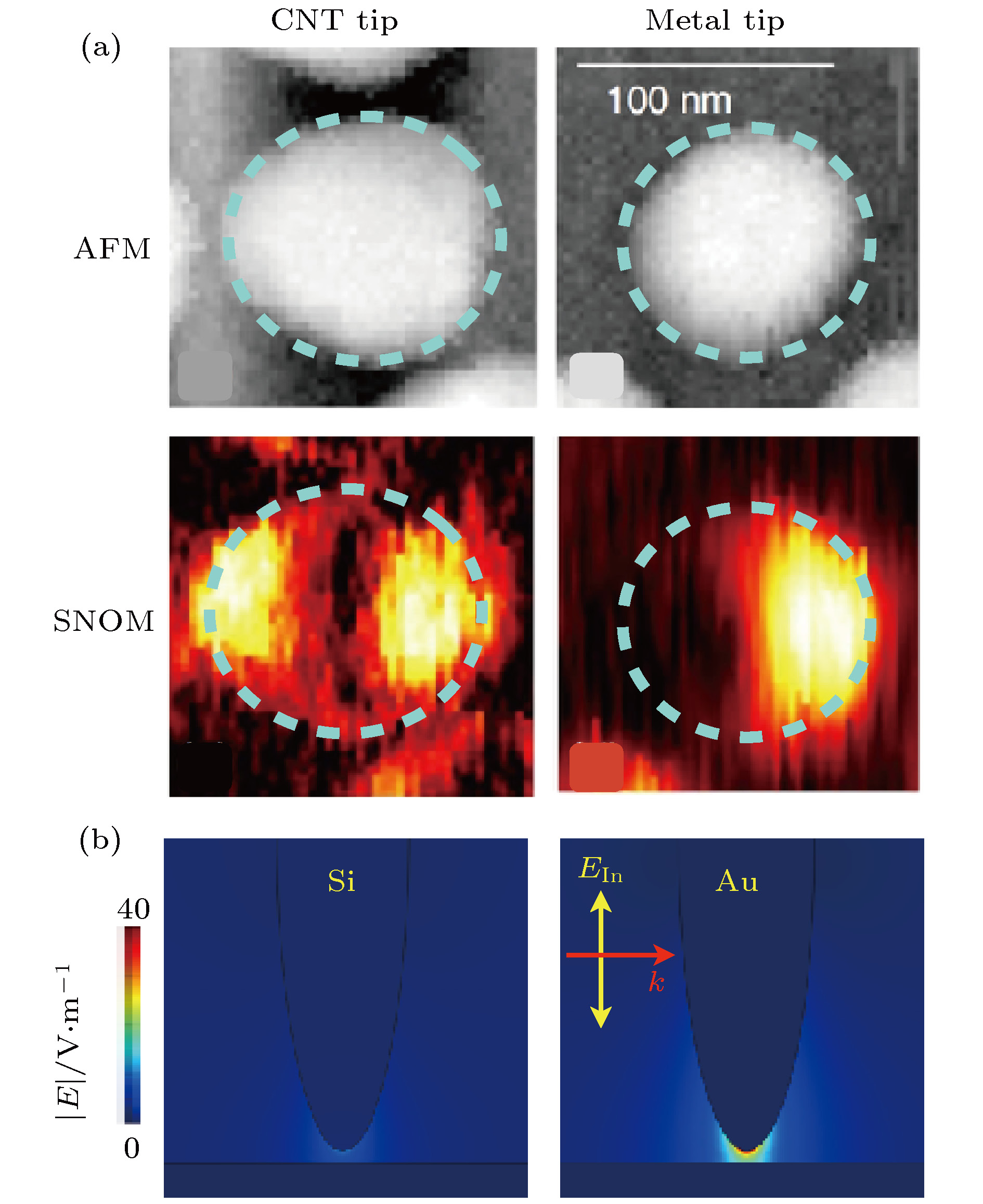 图 4 近场光学成像中金属探针和介质探针的比较 (a) 金纳米圆盘的形貌像和光学像, 分别由碳纳米管探针(CNT)和金属探针扫描所得[47], 标尺为100 nm; (b) 不同探针尖端局域电磁场的数值模拟结果
Figure4. The influence of AFM tip in near-field measurement: (a) Topography and near-field amplitude of a gold nanodisk obtained by carbon nanotube (CNT) tip and Pt-coated Si tip[47], the scale bar is 100 nm; (b) the numerical simulation of local electric field between AFM tip and substrate.
近场光学测量中另外一个重要的因素是光的偏振状态. 偏振状态一般由偏振片控制, 基于光波矢所在平面和针尖长轴方向的关系可分为S偏振和P偏振. 而入射偏振和检测偏振分别指入射光的偏振状态和探测器前收集光的偏振状态. 对入射偏振而言,


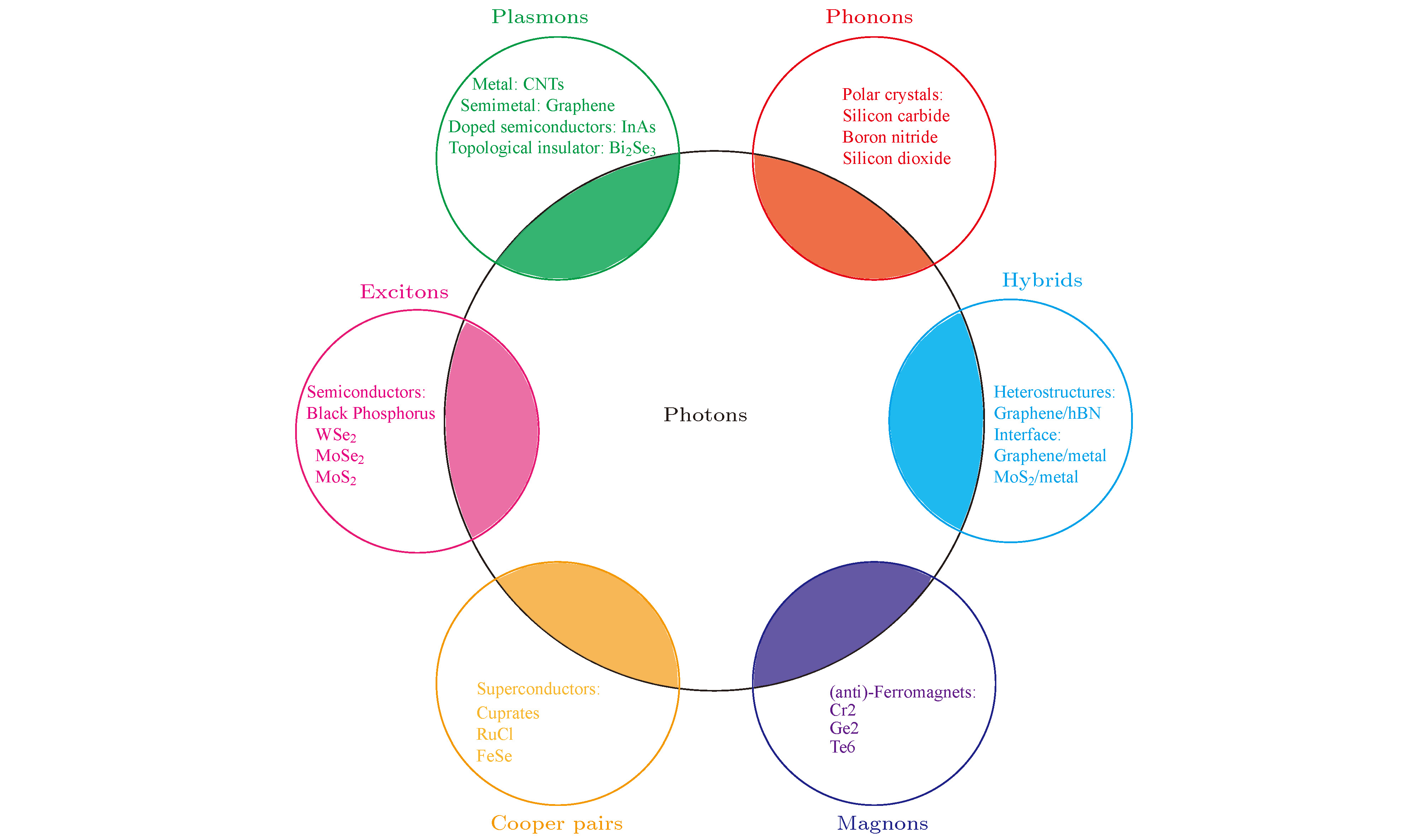 图 5 低维体系中的极化激元. 极化激元是光子和其他粒子或准粒子耦合后产生的一种玻色子, 包括富电子体系中的等离极化激元、极化晶体中的声子极化激元、半导体中的激子极化激元、超导体中的库珀对极化激元、铁磁体中的磁振子极化激元以及异质结中的杂化极化激元
Figure5. Polaritons in low-dimensional materials. Polaritons are collective excitation from coupling photons with other quasiparticles, such as plasmons in electron-rich systems, infrared-active phonons in polar insulators, excitons in semiconductors, cooper-pairs in superconductors, spin resonances in (anti)-ferromagnets and hybrids in heterostructures.
2
3.1.等离极化激元的近场光学研究
石墨烯[61,62]作为首个制备成功的二维原子晶体表现出独特的物理性质, 包括线性色散、常数光电导等[63,64]. 由于高度可调控的Drude权重和高的载流子迁移率, 石墨烯等离激元也具有一系列优良性质, 例如电压可控的色散行为, 超高局域因子(λ0/λp ≈ 50), 宽谱操作频率(中红外到太赫兹)和对外界条件的超灵敏性等. 近期, 一些近场光学实验不仅观察到了石墨烯等离激元的传播态和局域态, 而且实现了其散射行为的调控.由于石墨烯等离激元(


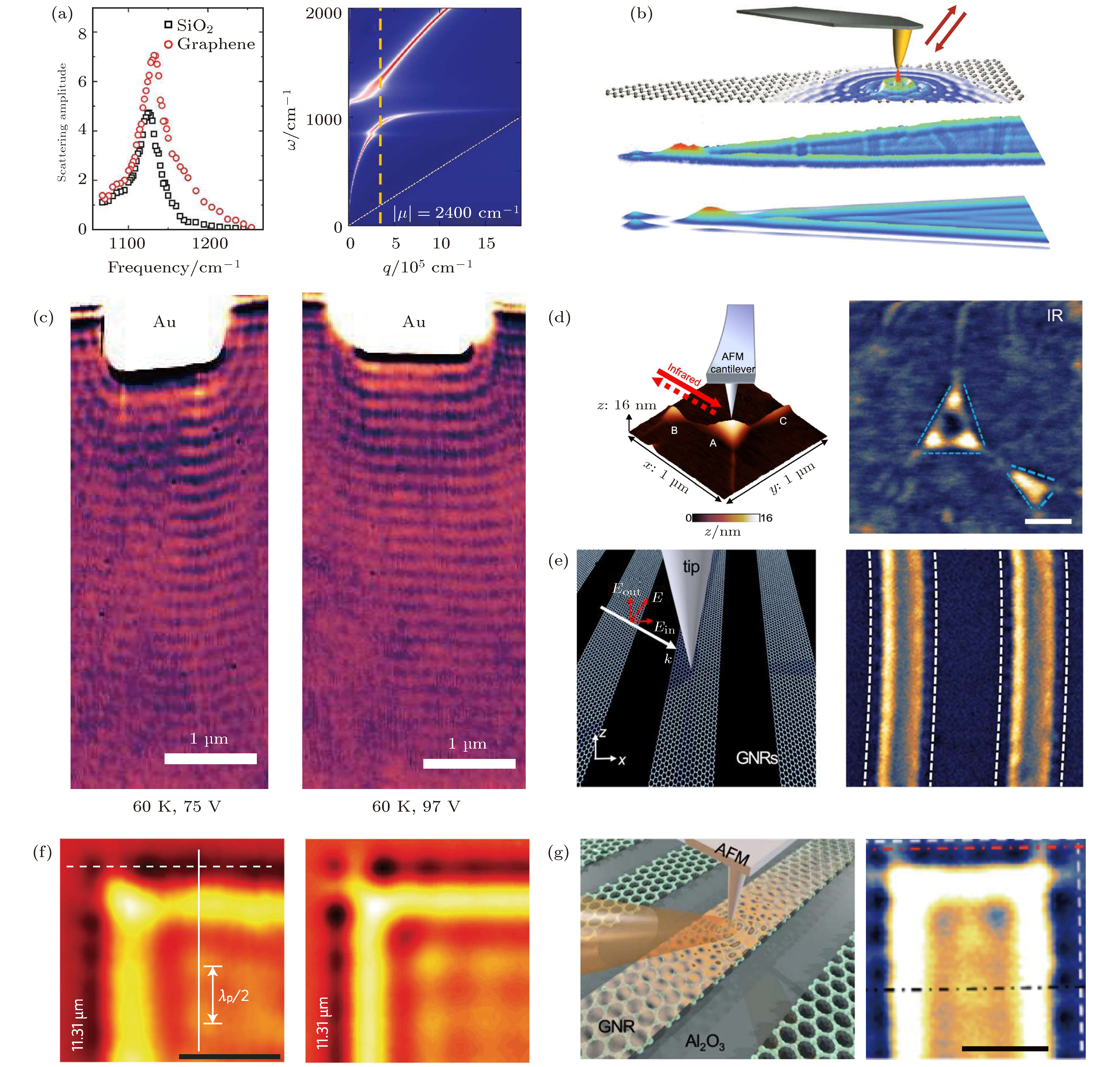 图 6 石墨烯中的表面等离极化激元 (a) 单层石墨烯中狄拉克等离激元的近场光谱测量及其色散的理论计算结果[67]; (b) 石墨烯等离激元的红外近场光学图像[68], 入射光波长为9.7 μm; (c) 液氮温区下石墨烯等离激元的近场光学图像[70], 入射光波长为11.28 μm; (d) 石墨烯纳米泡中等离激元局域“热点”[71], 入射频率为910 cm–1; (e) 石墨烯纳米带中等离激元传播态和局域态之间耦合产生的近场光学强度非对称现象[72], 入射频率为1184 cm–1; (f) 石墨烯方形谐振腔中等离激元一维边界模式和二维模式的近场光学测量及其数值模拟结果[74], 入射光波长为11.31 μm; (g) 石墨烯纳米条带中等离激元一维边界模式的近场光学成像[75], 入射光频率为1160 cm–1 (图(c) 中标尺为1 μm, 其他图中标尺均为200 nm)
Figure6. Surface plasmon polaritons in monolayer graphene: (a) Near-field spectroscopic measurement and theoretically calculated dispersion of Dirac plasmons in monolayer graphene[67]; (b) s-SNOM scheme (upper), experimental amplitude of graphene plasmons (middle) and calculated local density of optical states (bottom)[68], the incident wavelength is 9.7 μm; (c) nano-image of graphene plasmons launched by gold antenna under liquid-nitrogen temperature, the incident wavelength is 11.28 μm[70]; (d) plasmonic hot-spots inside graphene nanobubbles on boron nitride substrate[71], the incident frequency is 910 cm–1; (e) asymmetric plasmonic fringes induced by superposition of propagating and localized modes in graphene nanoribbons[72], the incident frequency is 1184 cm–1; (f) experimental (left) and calculated (right) near-field amplitude of graphene rectangle resonators, representing 1D edge mode and 2D sheet mode[74], the incident wavelength is 11.31 μm; (g) edge plasmons at the top boundary of graphene nanoribbons[75], the incident frequency is 1160 cm–1. Scale bars in all panels represent 200 nm, except for 1 μm in (c).
与半无限石墨烯中的等离激元传播模式相比, 石墨烯纳米结构中的局域模式[71-73]可以提供更强的局域因子和近场强度. 如图6(d)所示, Fei等[71]在石墨烯纳米泡中观察到了等离激元局域“热点”(hot-spot), 这对水环境中生物分子的红外光谱测量至关重要. 与传播模式相比, 这一局域模式拥有更大的局域因子(Vhot-spot/ ≈ 106)和更强的近场强度(两倍). 除此之外, Hu等[72]还在石墨烯纳米带中观察到了等离激元的不同模式. 如图6(e)所示, 当入射电场面内分量(EIn)垂直于石墨烯纳米带时, 可以同时激发表面传播型等离激元(SPP)和表面等离激元共振模(SPR), 而当电场分量平行于纳米带时, 只能激发传播型等离激元. 结合近场光学测量和数值模拟, 他们表明石墨烯纳米带中近场强度的不对称分布是由针尖激发的传播型等离激元和针尖增强的等离激元共振之间耦合产生的(图6(e)右).
由于石墨烯边界处的自由载流子只存在于边界一侧, 其Drude权重较小, 所以石墨烯等离激元的一维边界模式与二维传播模式相比表现出更弱的近场强度和更小的波长. 一般而言, 边界处的尖角结构和缺陷可以反射一维边界模式, 故其实空间成像常存在于经过光刻蚀之后的石墨烯结构中, 这是因为光刻蚀可以产生大量的边界缺陷, 而机械剥离制备的石墨烯边界是光滑的. 如图6(f)和图6(g)所示, 两个研究组[74,75]分别独立地观察到了石墨烯等离激元边界模式的基模和高阶模. 针尖激发的一维边界模式经尖角反射后形成法布干涉图样, 在近场光学图像中具体表现为周期性分布的暗点和亮点. 一维边界模式对电磁场有着超强的局域能力(λ0/60), 其体局域因子高达10–8. 通过数值模拟和近场测量, Nikitin等[74]解构了石墨烯纳米结构中的多种法布干涉模式, 包括边界模式, 二维平面模式和波导模式.
除单层石墨烯外, 双层石墨烯中也存在独特的等离激元现象. 双层石墨烯可以分为两种类型: 层间强耦合的Bernal堆叠型(bilayer)和层间弱耦合的随机堆叠型(double-layer)[76]. 与单层石墨烯相比, Bernal堆叠型石墨烯等离激元有更小的波长, 而随机堆叠型恰好相反. 此外, Bernal堆叠型存在层间量子隧穿效应, 故可观察到等离激元关闭区. 如图7(a)所示, Fei等[77]通过调控门电压实现了双层石墨烯等离激元的开关功能, 这对石墨烯场效应晶体管和等离激元通路光开关至关重要. 当入射波数为883 cm–1时, 等离激元的关闭区域可达约50 V. 另一近场光学实验[76]表明, Bernal堆叠型和随机堆叠型双层石墨烯中的本征声子偶极模是不同的(图7(b)). 如图7(b)左所示, 随机堆叠型石墨烯中的反转对称性抵消了诱导电荷, 从而产生了具有拉曼活性的光学声子峰1580 cm–1. 而在Bernal堆叠型中反转对称性遭到破坏, 故存在红外活性的光学声子峰1580 cm–1. 在不同堆叠类型的高掺杂双层石墨烯中, 光学实验和理论模拟都给出了不同的等离激元色散关系. 可以看到Bernal堆叠型中等离激元色散关系在1580 cm–1处有明显的交叉现象, 这表明此处存在红外活性声子. 如图7(b)内插图所示, 近场光学图像表明等离激元和红外活性光学声子之间的相互作用会极大地减小其寿命.
 图 7 双层石墨烯中的等离激元 (a) 左: 单层石墨烯和双层石墨烯中等离激元随施加电压的变化趋势; 右: 双层石墨烯中光电导随电压变化趋势的理论计算结果, 图中箭头表示等离激元关闭区域[77]; (b) 随机堆叠型(左) 和Bernal堆叠型(右) 双层石墨烯中等离激元与声子之间相互耦合作用的近场光学测量[76]. 散点代表实验数据, 背景色为菲涅耳反射系数虚部的理论计算结果. 内插图为石墨烯等离激元的近场光学图像
Figure7. Plasmon polaritons in bilayer graphene: (a) Left panel: experimental measurement of voltage-dependent plasmonic wavelength in monolayer (SLG) and bilayer (BLG) graphene. Right panel: Theoretical calculation of voltage- and frequency-dependent imaginary part of the optical conductivity. The double-headed arrows indicate plasmon-off region of bilayer graphene[77]; (b) near-field study of interaction between plasmons and intrinsic phonons in highly doped double-layer (left) and bilayer graphene (right)[76]. The dispersed symbols represent experimental data and background color indicates the imaginary part of the calculated Fresnel reflection coefficient. Inset: representative near-field images of graphene plasmons and corresponding symmetry of phonon-induced charge densities.
迄今为止, 石墨烯等离激元的应用主要基于其独特的物理性质, 包括电压可控的Drude权重和与其他极化激元之间的强耦合作用. 如图8(a)所示, 近场测量表明[78], 通过调控所施加的电压范围, 石墨烯可以实现纳米级(350 nm)的等离激元调制器, 达到


 图 8 石墨烯等离激元的应用 (a) 基于石墨烯等离激元的红外光相位调制器[78], 上图为实验原理图, 下图为
Figure8. The applications of graphene plasmons: (a) Phase control of infrared light by gate-tunable graphene plasmons[78]. Upper panel: schematic of experimental configuration. Bottom panel: Theoretical (solid lines) and experimental (dispersed circles) phase shift, which can be changed from 0 to

2
3.2.声子极化激元的近场光学研究
由于传统各向同性材料中的介电张量为常数, 所以波的等频面是一个球面, 其波矢大小在各个方向都相等. 不同的是, 在双曲线型材料中, 介电张量在面内(

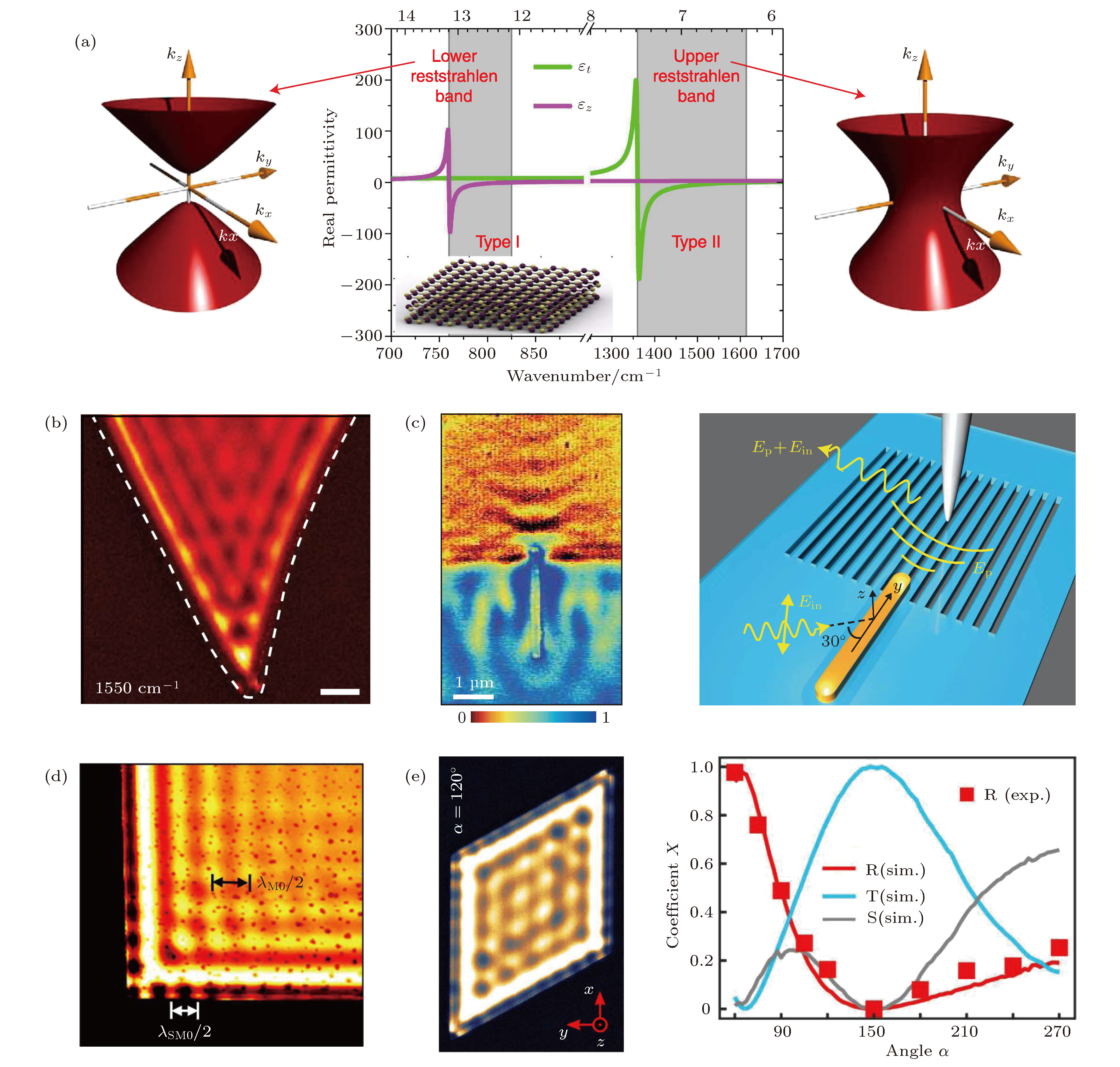 图 9 氮化硼中双曲线型声子极化激元 (a) 天然氮化硼晶体中的双曲线行为, 其等频面为两类双曲面[80]; (b) 氮化硼晶体中双曲线型声子极化激元的近场光学图像[56], 入射光频率为1550 cm–1, 标尺为800 nm; (c) 氮化硼超表面面内双曲线型声子极化激元的近场光学图像[88]; (d) 氮化硼中表面局域声子极化激元(HSPs) 的近场光学图像[90], 入射光频率为1420 cm–1, 标尺为2 μm; (e) 不同角度氮化硼中HSPs的散射行为[91]
Figure9. Hyperbolic phonon polaritons (HPPs) in boron nitride: (a) Hyperbolic behavior of natural hBN crystal, which gives two separate spectral bands called lower and upper Reststrahlen bands with opposite-signed in-plane (


Dai等[56]首次实现了氮化硼中双曲线型声子极化激元的实空间成像, 并研究了其物理性质, 例如波长、传播损耗和色散行为等. 声子极化激元来源于氮化硼中光学声子和光子的相互作用. 如图9(b)所示, 针尖激发的声子极化激元以球面波的形式向外传播, 在氮化硼边界处反射, 二者形成平行于边界的干涉驻波, 周期为极化激元波长的1/2. 实验和理论都表明声子极化激元波长依赖于氮化硼晶体的厚度. 与石墨烯等离激元相比(λ0/λp ≈ 50, γ ≈ 0.15), 氮化硼声子极化激元拥有相似的局域因子(λ0/λp ≈ 25)和更低的传播损耗(γ ≈ 0.055), 这是因为声子极化激元在绝缘体中可以有效避免电子散射带来的传播损耗. 然而, 氮化硼是面内各向同性材料, 也就是说其双曲线行为只存在于面外方向. 为了观察面内各向异性, Li等[88]通过微纳加工方式制备了氮化硼超表面结构. 如图9(c)所示, 他们利用散射型SNOM观察到了曲面的声子极化激元波前, 这意味着得到了面内各向异性结构. 近期, 科学家还发现氧化钼是一种天然的面内各向异性材料, 在中红外波段可以支持面内双曲线型声子极化激元[89]. 他们观察到氧化钼晶体中声子极化激元的等频面可以从椭圆变为双曲线型, 最高寿命可以达到8 ps左右, 这一数值是常温下石墨烯等离激元的十倍, 低温下石墨烯等离激元的四倍. 观察到的超低损耗面内各向异性声子极化激元为今后纳米级能量定向传输和光与物质相互作用调控提供了新思路.
如果将氮化硼光轴方向旋转90°, 可以得到另一种表面局域的声子极化激元(HSPs)[90]. 对于机械剥离制备的氮化硼来说, 其光轴方向垂直于晶体表面, 故针尖在晶体内部无法激发HSPs. 然而, 当针尖处于边界上方时可以在边界处激发HSPs, 如图9(d)所示. 与体局域声子极化激元相比, HSPs拥有更强的场局域特性、更小的群速度、几乎相同的寿命和外界环境敏感性. 此外, HSPs的散射行为受到氮化硼晶体角度的影响. 如图9(e)所示, Dai等[91]通过改变不同的氮化硼角度调控了HSPs的传播特性, 从全透射到全反射. 当然, HSPs与体局域声子极化激元之间复杂的干涉现象需要进一步研究.
由于面外定向传播[92]和超高的品质因子, 氮化硼声子极化激元在多个领域中有重要应用, 例如超分辨成像(图10(a))、亚波长聚焦(图10(b))和介质纳米天线(图10(c))等. 如图10(a)所示, Li等[92]在实验和理论上表明, 可以通过改变入射光频率调控氮化硼声子极化激元的面外传播方向, 从而得到突破衍射极限的双曲透镜. 他们实现了氮化硼晶体底部金纳米结构的放大或等比例成像, 都突破了传统衍射极限. 在图10(b)中, Dai等[93]利用氮化硼声子极化激元面外定向传播的性质实现了中红外光的纳米聚焦, 焦点直径约为入射光波长的1/100. 如图10(c)所示, 近场光学实验[94]还揭示了介质氮化硼天线中声子极化激元的Fabry-Perot共振, 其品质因子高达100. 通过结合数值模拟中的模式分析和近场测量, Alfaro-Mozaz等[94]表明Fabry-Perot共振来自于杂化的HSPs而非体局域的声子极化激元. 在不同长度的氮化硼天线中, 他们观察到了和传统贵金属天线相似的极化激元模式分布, 但具有更高的品质因子和Purcell效应.
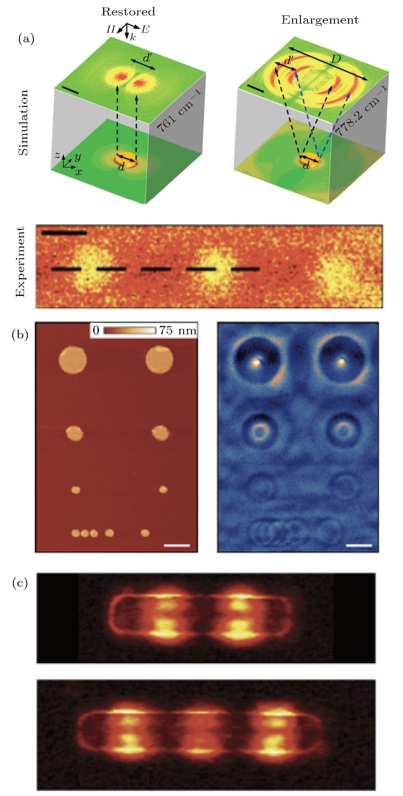 图 10 双曲线型声子极化激元的应用 (a) 基于氮化硼声子极化激元的超分辨成像[92], 上: 数值模拟; 下: 近场光学测量; (b) 基于氮化硼实现中红外光的纳米聚焦[93], 标尺为1 μm; (c) 不同长度氮化硼线性天线的近场光学图像[94], 上: 长度为1327 nm; 下: 长度为1713 nm
Figure10. The applications of hyperbolic phonon polaritons: (a) Near-field imaging and nano-focusing realized by hBN-HPPs[92]. Upper panel: simulated perfect imaging (ω0 = 761 cm–1) and enlarged imaging (ω0 = 778.2 cm–1) of gold nanodisk beneath the hBN crystal. Bottom panel: experimental nano-infrared images of gold nanodisk beneath hBN with the broadband incident laser; (b) sub-wavelength focusing of mid-infrared light through an hBN crystal[93]. Left panel: AFM image of gold disks on SiO2/Si substrate before hBN transfer. Right panel: near-field amplitude on the top of hBN crystal with incident frequency at 1515 cm–1. Scale bar, 1 μm; (c) linear hBN dielectric antenna with different lengths[94], 1327 nm in upper panel and 1713 nm in bottom panel. The incident frequency is 1432 cm–1.
2
3.3.激子极化激元的近场光学研究
激子极化激元是指广泛存在于半导体中的激子与光子耦合之后形成的极化激元. 过渡金属硫族化合物(TMDs)[95]经过机械剥离后形成一类重要的二维范德瓦耳斯半导体材料, 它们具备可控的带隙宽度和强耦合激子. 近场实验在多种二维TMDs材料中观察到了激子极化激元. Fei等[96]和Hu等[97]首次在二硒化钨(WSe2)和二硒化钼(MoSe2)中观察到了激子极化激元的面内模式和面外模式, 如图11(a)和图11(b)所示. 近场光学图像清晰地展示了激子极化激元形成的干涉驻波, 并且可以直接测量其物理性质, 例如波长、色散关系和传播长度等等. 激子极化激元的波导模式拥有超长的传播距离(12 μm左右), 独特的回弯色散关系以及晶体厚度依赖性. 半导体范德瓦耳斯晶体中的激子极化激元共振频率一般为近红外波段, 这正好填补了石墨烯等离激元(中红外到太赫兹)和贵金属等离激元(可见光波段)之间的空白. 图 11 半导体中激子极化激元的近场光学成像 (a) 二硒化钨中激子极化激元的近场光学图像[96], 白色虚线为二硒化钨的边界; (b) 二硒化钼中激子极化激元的近场光学图像[97], 图中标尺为1 μm
Figure11. Near-field studies of exciton polaritons in semiconductors: (a) Representative near-field image of a WSe2 flake, whose edges are marked by white dashed lines[96]; (b) near-field image of exciton polaritons in planar MoSe2 waveguide at laser energy of 1.41 eV[97]. Scale bar is 1 μm.
2
3.4.杂化极化激元的近场光学研究
从2004年石墨烯制备成功开始, 科学家已经发现了多种类型的二维原子晶体, 其性质涵盖了超导体、半金属、半导体、绝缘体等. 这些多种多样的原子晶体可以作为一种单体进行组合, 得到范德瓦耳斯异质结, 这也是人类第一次在原子尺度上制备材料并调控其性质. 迄今为止, 近场光学成像揭示了范德瓦耳斯异质结中的杂化极化激元, 也为今后新型极化激元的开发和二维极化激元学的发展指明了方向. 如图12(a)所示[98], 利用氮化硼可以有效地避免传统二氧化硅衬底光学声子对石墨烯等离激元的散射作用, 从而减小其传播损耗. 由于氮化硼与石墨烯的晶格结构非常类似, 氮化硼可以成为有效的缓冲层, 在两层氮化硼保护下, 石墨烯等离激元可以获得超长寿命(500 fs)和更高的局域因子(150). 与此不同的是, Yang等[99]还发现氮化硼声子极化激元和石墨烯等离激元可以耦合, 形成杂化的声子等离激元极化子(图12(b)). 远场红外光谱和近场成像都表明氮化硼/石墨烯异质结中极化激元寿命的增大来自于石墨烯等离激元和单层氮化硼晶体面外光学声子横模之间的耦合作用. 这种新的杂化极化激元具有超长的寿命(1.6 ps), 也为我们提供了一种在频域和时域调控石墨烯等离激元的思路.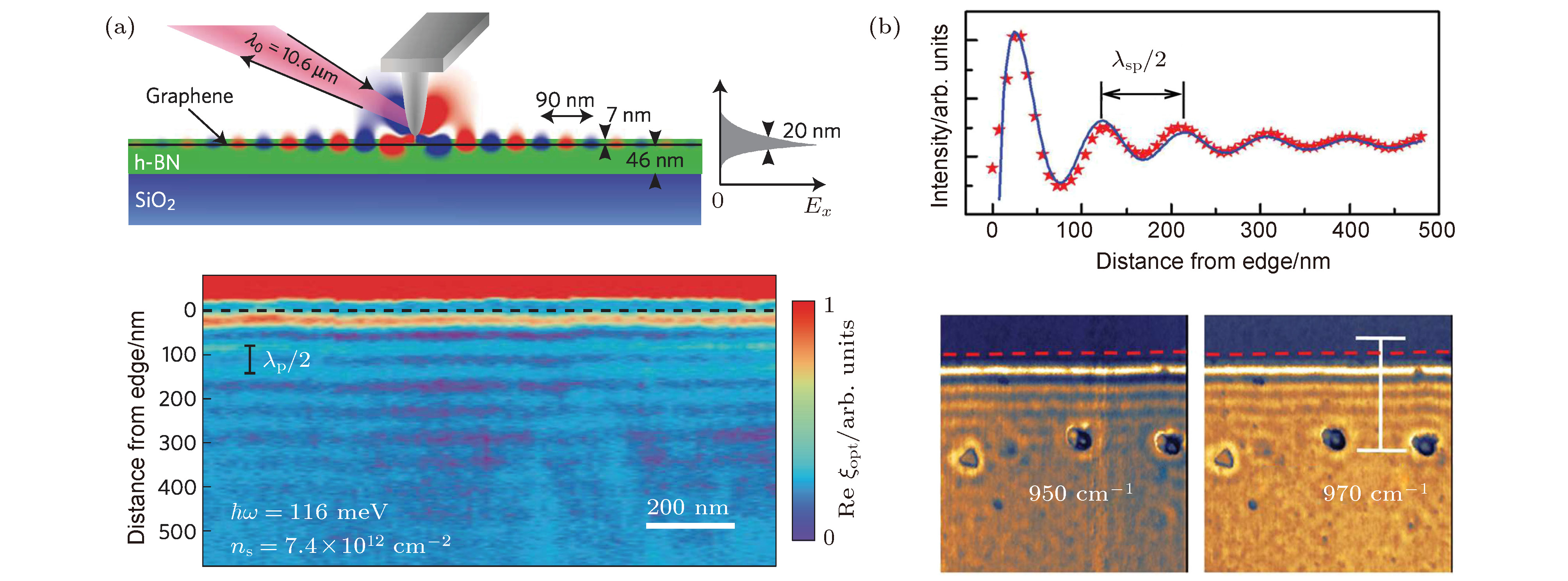 图 12 范德瓦耳斯异质结中的极化激元 (a) 氮化硼/石墨烯/氮化硼异质结中超低损耗等离激元的近场光学成像[98], 黑色虚线为石墨烯边界, 入射光波长为10.6 μm; (b) 石墨烯/氮化硼中杂化等离–声子极化激元的近场光学成像[99], 红色虚线为石墨烯边界 (图中标尺为500 nm)
Figure12. Polaritons in van der Waals heterostructures: (a) Near-field image of low-loss graphene plasmons in hBN/Graphene/hBN heterostructures[98]. Upper panel: Side-view sketch of near-field measurement of back-gate graphene encapsulated by hBN layers. Bottom panel: representative near-field image with incident wavelength at 10.6 μm. The graphene edge is marked as black dashed line. (b) Hybridized plasmon-phonon polaritons in graphene/hBN heterostructures[99]. Upper panel: experimentally extracted wavelength of plasmon-phonon polaritons. Bottom panel: representative near-field images of polaritons. The graphene edge is marked by red dashed lines. The incident frequency is 950 cm-1 and 970 cm-1, respectively. Scale bar is 500 nm.
 图 13 超快近场光学 (a) 实验测量氮化硼声子极化激元的动力学参数[100], 黄色区域代表金天线, 内插图显示了极化激元波的传播, 右图为不同延迟时间下的极化激元波包, 黑色和绿色实线分别代表群速度和相速度; (b) 石墨烯抽运-探测近场光谱图[103], 从左到右探测光与抽运光之间的延迟分别为0, 200和400 fs, 标尺为1 μm; (c) 石墨烯中光诱导等离激元的超快光学成像[104]
Figure13. Ultrafast near-field optics. (a) The experimentally extracted propagation of type-1 HPPs in the space-time domain[100]. The yellow region represents the gold antenna launching polaritons. The inset shows zoom into the fringe patterns. Right panel: the line profiles for different time delays. The black and green solid lines show the envelope of the fringe patterns (group velocity) and intrinsic fringe patterns (phase velocity), respectively. (b) Near-infrared (NIR) pump-induced changes in the near-field amplitude of graphene for different pump-probe time delays[103]. The pump and probe lasers are 1.56 μm and broadband mid-infrared pulses, respectively. The dark region in near-field images represents SiO2 substrate. Different optical contrast is caused by different layered graphene. Scale bar, 1 μm. (c) Ultrafast controlling of photo-induced plasmon polaritons in graphene encapsulated by two hBN layers[104]. Left panel: the schematic of pump-probe s-SNOM set-up. Right panel: the two-dimensional hyperspectral map of photo-induced plasmons in hBN/graphene/hBN device. The black solid line gives the edge of device. The pump laser is at 1.56 μm. The probe beam spans frequencies from 830–1000 cm–1.
除了时间分辨率和空间分辨率外, 化学分辨率也对研究光与物质的相互作用至关重要. 传统的傅里叶转换红外光谱(FTIR)[105]经常用来测量分子的光谱信息和识别二维材料中的极化激元共振峰, 其空间分辨率受限于经典的衍射极限, 一般为微米级. 而通过将远场红外光谱与近场成像技术结合, 可以在保证化学分辨率的同时得到纳米级的空间分辨率, 已经在二维极化激元的研究中广泛应用[106-110]. 与一般的单频率近场成像相比, 宽谱的近场成像具有更宽的成像波段和更快的成像速度. 此外, Huth等[111]还研究了纳米红外光谱与样品局域介电响应之间的关系, 为今后纳米区域内化学分子的识别提供了理论基础. 如图14(a)所示, 聚甲基丙烯酸甲酯(PMMA)的近场红外吸收峰与传统远场红外吸收峰对应良好, 这说明纳米红外光谱可以有效探测所有红外活性的分子振动峰. 其高达20 nm的空间分辨率可以帮助我们识别纳米区域内的污染物, 例如聚二甲基矽氧烷(PDMS), 这对于今后材料的制备和局域极化激元的研究有着非常重要的作用.
 图 14 近场光学成像的发展 (a) 通过散射型SNOM和红外光谱结合测量纳米区域化学分子的红外光谱[111]; (b) 共振金天线激发石墨烯等离激元的近场光学图像[112]; (c) 非共振金天线激发氮化硼声子极化激元的近场光学图像[113], 图中标尺为1 μm
Figure14. Development in near-field optics. (a) Chemical identification of nanoscale sample contaminations with nano-FTIR, which is combination of s-SNOM and Fourier transform infrared spectrum (FTIR)[111]. Left panel: Topography image of poly-(methyl methacrylate) thin film (PMMA, marked as A on silicon substrate, with a contaminated particle of polydimethylsiloxane (PDMS, marked as B. Right panel: corresponding absorption spectra of PMMA (taken from spot A) and PDMS (taken from spot B). (b) Near-field imaging of plasmonic wavefront launched by gold antenna, instead of AFM tip[112]. Upper panel: AFM topography images of fabricated gold antenna. Bottom panel: representative near-field image of plasmonic wavefront with incident wavelength at 11.06 μm. (c) Near-field imaging of wavefront of hBN-HPPs launched by gold antenna[113]. The brighter region represents gold antenna, encapsulated between hBN and SiO2 substrate. Scale bar is 1 μm.
二维极化激元学的近场研究面临的另外一个瓶颈就是成像机理问题. 为了获得增强的近场光学信号和足够的动量补偿, 在二维范德瓦耳斯材料中极化激元的探测通常使用金属针尖. 如本文2.3节所述, 金属针尖尖端存在很强的局域电磁场, 在近场成像中同时扮演着激发源和探测源的角色, 即针尖激发的极化激元波向外传播, 碰到界面反射后与原波产生干涉, 产生平行于反射界面的驻波. 故在近场光学图像中, 针尖激发的极化激元总是表现为平行于界面的驻波, 这将导致两个问题.
其一, 无法得到极化激元的波前信息. 例如在石墨烯[68,69]和氮化硼[56](面内各向同性材料)中, 偶极子激发的极化激元波前应为球面波, 在氧化钼[89](面内各向异性材料)中, 偶极子激发的极化激元波前应为双曲面或椭球面, 但二者在金属针尖扫描的近场光学图像中均表现平行于边界的干涉驻波条纹. 其二, 由于针尖在逐点扫描, 干涉过程涉及复杂的物理过程. 例如在研究极化激元的折射现象时, 针尖激发引起的干涉使得波的传播非常复杂难解. 再例如极化激元在不同的反射界面反射率和相位延迟不一样, 这给后续的数据解读也带来了困难. 为了解决这些问题, 需要寻找能够代替金属针尖来有效激发极化激元的天线. 如图14(b)所示, Alonso-González等[112]表明共振的金天线可以在天线尖端处提供强的局域电磁场和大的动量补偿, 从而有效地激发石墨烯等离激元, 其波前随着天线形状发生变化. 在此基础上, Duan等[113]表明非共振天线(图14(c)), 例如材料本身的几何突起和金属结构, 也可以提供足够的动量补偿来激发氮化硼声子极化激元. 与针尖激发的极化激元相比, 非干涉成像的极化激元拥有可控的波前形状和更低的传播损耗.
1)进一步改善空间、时间和化学分辨率. 为了在原子尺度上研究物理现象, 需要进一步提高近场成像技术的空间分辨率, 也就是说, 要进一步减小所使用针尖的尺寸. 可能的针尖有碳纳米管针尖, 单分子针尖, 甚至单原子针尖. 当然, 在减小针尖尺寸的同时还必须增强针尖散射效率, 以便提高近场成像的信噪比. 此外, 功能性针尖也为我们提供了一个新的自由度去调控物质的光学性质, 如图15(a)所示, 对于碳纳米管针尖而言, 不同的化学组成[114]可以有效改变针尖的极化率, 从而调控近场成像过程. 将来, 近场成像与阿秒技术的结合可以帮助我们研究原子的光学现象. 通过将近场成像与传统光谱技术例如红外光谱或拉曼光谱结合, 科学家同时实现了纳米级空间分辨率和化学分辨率. 原则上讲, 近场光学成像技术可以与更多的表征手段耦合, 在保证纳米级空间分辨率的同时发展更高的化学分辨率, 例如将散射型SNOM与质谱[115]结合. 如图15(c)所示, SNOM和质谱的耦合可以提供纳米级的空间分辨率和对化学键、化学组分的高灵敏检测;
 图 15 近场光学前景展望 (a) 化学合成的碳纳米管结构[114], 其光学性质可以通过化学组分有效调控; (b) 开口环形探针可用于近场磁场面内和面外分量的测量[51], 图中标尺为500 nm; (c) 散射型SNOM与质谱耦合, 可同时得到纳米级空间分辨率和超高化学分辨率; (d) 极端环境下SNOM的发展, 包括超低温、强磁场和超高真空等
Figure15. The perspective of near-field optics: (a) Chemically fabricated carbon nanotube cup, whose properties can be effectively controlled by chemical component[114]; (b) split-ring probe is sensitive to both in-plane (Hx or Hy) and out-of-plane (Hz) component of near-field magnetic field[51], scale bar, 500 nm; (c) the combination of near-field optics and mass spectroscopy for highly chemical resolution and spatial resolution, simultaneously; (d) the developed s-SNOM in extreme environment, including ultralow temperature, strong magnetic field and ultrahigh vacuum.
2)定量测量纳米空间光矢量场. 众所周知, 由完整的近场电磁场分布信息可以准确推断出材料的远场光学性质, 这一理论被称为“远场转换光学”(far-field transformation). 所需的信息为近场分布的所有矢量场数值, 包括电场分量(Ex, Ey, Ez)和磁场分量(Hx, Hy, Hz). 如果六个数值中的任意三个可以实验测量, 就可以通过麦克斯韦方程组计算出整个矢量场. 然而, 同时测量三个矢量信息是一项非常有挑战性的工作[116,117], 尤其是磁场分量和相位信息. 如图15(b)所示, 迄今为止, 只有孔径型SNOM中的环形针尖可以实现面内和面外磁场分量的测量[51]. 今后需要去设计特殊的针尖去探测纳米空间中光矢量场的全部分量信息.
3)极端环境中光学现象的研究. 在极端条件下有许多独特的物理现象, 例如超低温环境中的超导转变, 强磁场中的量子霍尔效应, 超高真空中的界面物理等. 与此同时, 物质在低温下展现出很多特殊性质, 例如大的电子平均自由程和拓扑保护态等. 如图15(d)所示, 极端条件下的近场光学成像技术为量子物理的发展打开了新的大门.
4)近场光学理论的完善. 由于针尖和样品之间存在着复杂的相互作用, 近场光学图像的理解常常基于数值模拟, 而非解析解. 与此同时, 近场光学成像中一些复杂效应的影响还没有研究清楚, 例如多体效应、量子效应、非局域效应等.
为了解决这些问题, 需要发展更加精准的近场光学理论体系.
