

全文HTML
--> --> -->过去几年, 理论预言了一些内禀磁性拓扑绝缘体, 包括MnBi2Te4家族系列[7-9]以及EuIn2As2, EuSn2As2, EuSn2P2等含Eu系列材料[10-12]. 其中, EuIn2As2具有内禀的反铁磁序, 早先的磁测量结果显示它的磁结构可能是A型反铁磁, 即Eu原子在层内是铁磁耦合, 相邻Eu层之间是反铁磁耦合, 材料的反铁磁转变温度TN约为18 K[13-16]. 理论预言在反铁磁相下它是轴子绝缘体, 磁性原子的自旋取向决定了它所处的拓扑态: 当自旋沿着ab面内时, 它是具有无能隙表面态的拓扑晶体绝缘体; 当沿着c方向时, 它是具有一维棱态(hinge state)的高阶拓扑绝缘体[10]. 最新的中子衍射实验认为, EuIn2As2可能具有更复杂的螺旋形反铁磁序, 具有

本文利用STM, 研究了EuIn2As2单晶解理表面的结构. STM形貌图表明, 材料的解理面以条纹状的有序结构为主, 结合原子分辨的STM形貌图、晶格对称性分析以及扫描隧道谱(scanning tunneling spectroscopy, STS) 信息, 认为条纹面起源于Eu截止面50%覆盖度形成的表面重构. 通过对条纹面态密度的测量, 发现费米能附近的态密度随温度的演化与反铁磁相变有很强的关联特征. 此外, 在台阶边缘附近偶尔观测到少量迷宫状结构, 通过分析原子像与台阶高度, 认为它可能是Eu原子形成的翘曲结构. 作为表面能带计算与实验观测的桥梁, 对表面结构的测定为理解EuIn2As2的表面电子结构以及拓扑性质提供了重要线索.
测量所用仪器是一台自主搭建的低温扫描探针显微镜, 兼具扫描隧道显微镜与原子力显微镜(atomic force microscope, AFM) 的功能. 样品在低温超高真空环境下解理, 解理温度约20 K. 如不加特殊说明, 扫描头的基础温度是4.2 K. 实验使用电化学腐蚀的W针尖, 并在Au靶上做场发射处理. STM形貌图在恒流模式下获取. STS采用标准的锁相放大技术获取, 调制电压频率为781.1 Hz. AFM测量基于qPlus传感器, 采用非接触调频模式.
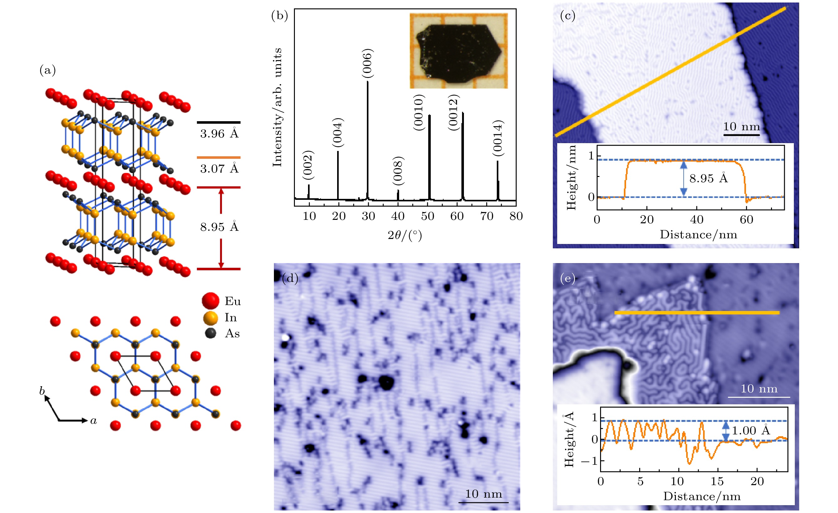 图 1 EuIn2As2的晶格结构和表面形貌 (a) EuIn2As2的晶格结构示意图, 图中所示Eu—Eu, Eu—In, In—As原子层间距分别是8.95, 3.07, 3.96 ?; (b) EuIn2As2的X射线衍射图案, 插图是典型EuIn2As2单晶的照片; (c) 包含台阶的大范围STM形貌图(Vs = 1 V, I = 100 pA), 插图是沿着图中黄线所标示位置的高度轮廓, 台阶高度8.95 ?, 与晶格常数的一半 c/2 = 8.95 ? 一致; (d) 典型的条纹面STM形貌(Vs = 1 V, I = 1 nA); (e) 包含迷宫状结构的STM形貌图 (Vs = –200 mV, I = 20 pA), 图中左下角为上层台阶, 右侧为条纹面, 插图是沿着图中黄线所标示位置的高度轮廓, 迷宫面与条纹面高度差约1 ?
Figure1. Crystal structure and surface morphologies of EuIn2As2. (a) Schematic crystal structure of EuIn2As2, where the interlayer distance Eu—Eu, Eu—In, and In—As is 8.95, 3.07, and 3.96 ?, respectively. (b) X-ray diffraction pattern of EuIn2As2 crystal. The inset is a picture of typical EuIn2As2 single crystal. (c) Large scale STM topography showing step edges (Vs = 1 V, I = 100 pA). Inset is the height profile along yellow line, the step height is 8.95?, which is consistent with half unit cell c/2 = 8.95 ?. (d) STM topography of typical stripe surface (Vs = 1 V, I = 1 nA). (e) STM topography containing a maze-like structure (Vs = –200 mV, I = 20 pA), which is located between a higher step (left bottom) and a stripe surface (right part). The inset is the height profile along yellow line. The step height between maze-like surface and stripe surface is about 1 ?.
图1(c)是解理后的EuIn2As2样品表面的STM形貌图. 可以看到, 图中存在一个凸台状的台阶, 图1(c)中的插图显示了形貌图中沿黄线的高度轮廓, 可以看到台阶的高度约为8.95 ? = c/2. 经过大量观测, 绝大多数相邻台阶的高度差为c/2或其整数倍. 台阶表面是亮暗条纹构成的有序结构, 如图1(d)所示, 以下称之为条纹面. 极少数情况下, 观测到一种条纹方向多变、形似迷宫的表面, 以下称之为迷宫面. 如图1(e)所示, 左下角高亮的区域是上层台阶, 下层台面最右侧是常见的条纹面, 在条纹面与上层台阶之间是迷宫面. 两种表面沿着黄线的高度轮廓如图1(e)的插图所示. 可以看到迷宫面起伏较大, 亮暗条纹高度差约1 ?, 而条纹面起伏小, 亮暗条纹高度差约0.1 ?. 简洁起见, 以下用迷宫面亮条纹的高度指代迷宫面的高度. 迷宫面比条纹面高约1 ?, 迷宫面的暗条纹与条纹面表观高度相当.
如果材料解理时, 两种可能断键的位置(In—In键和Eu—As键) 都发生断裂, 将会出现复杂的台阶高度, 如In和Eu面的台阶高度3.07 ?, In和As面的台阶高度3.96 ?等, 如图1(a)所示, 大量实验中从未观测到这些台阶高度. 因此可推测样品只在In—In或Eu—As中一处断键. 为了探究解理面的截止情况, 本文对两种表面结构做了详细的研究.
图2(a)是条纹面上获得的STM形貌图, 可以看到亮条纹覆盖整个表面. 条纹上存在一些转折和空洞构成的断点, 这导致亮条纹表现为不连续的线段. 但条纹整体呈现一定的方向性, 这种方向性可以在微米尺度保持. 图2(b)是同一区域的原子分辨STM形貌图, 亮条纹内原子间距为晶格常数a, 亮条纹间原子间距约7.27 ?, 这个数值符合EuIn2As2面内六角格子的次近邻原子间距

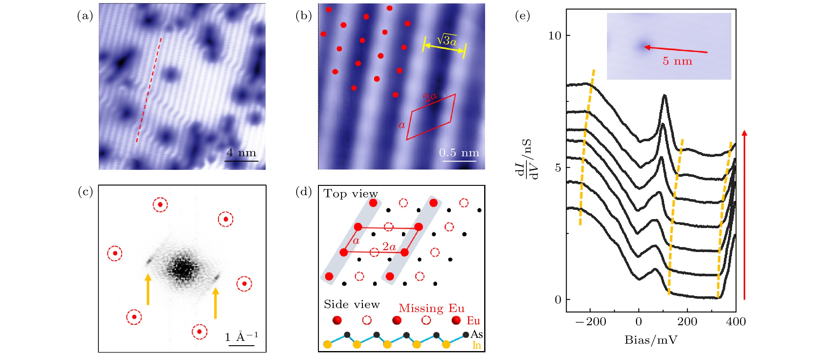 图 2 条纹面的结构 (a) 条纹面的STM形貌 (Vs = 1 V, I = 200 pA), 沿图中红色虚线条纹转折一次错位半个周期, 深蓝色区域为表面缺陷; (b) 条纹面的原子分辨像 (Vs = –2 mV, I = 1 nA), 红色平行四边形表示重构后的原胞, 红色点阵代表面内晶格格点; (c) 图(a)的FFT, 黄色箭头所示为条纹的周期, 红色圆圈标注的六个红点代表图(b)所标注六角格子的布拉格点; (d)条纹面的原子排布示意图, 暗红色球代表观测到的Eu原子, 红色虚线圆圈代表亮条纹之间丢失的Eu原子, 黑色/黄色点代表Eu层以下的As/In原子; (e)跨条纹面上空位缺陷的STS谱, 插图中红线标出了测谱位置, 测谱条件为Vs = 400 mV, I = 200 pA, 调制电压幅度5 mV, 图中黄色虚线帮助示意STS曲线中的特征随空间的演变
Figure2. Structure of stripe surface. (a) STM topography of stripe surface (Vs = 1 V, I = 200 pA), the stripe shifts half unit cell along the red dashed line. Dark blue areas are surface defects. (b) Atomic resolved STM image of stripe surface (Vs = –2 mV, I = 1 nA), the red parallelogram shows the doubled unit cell, the red spots are superposed in-plane lattice structure. (c) FFT image of panel (a). The stripe modulation is marked by yellow arrows. The superposed six red dots marked by dashed red circles are the simulated Bragg points of the inserted hexagonal lattice in panel (b). (d) Schematic drawings of atomic arrangement on the stripe surface. Dark red spheres show the observed Eu atomic chain, dashed red circles show the missing Eu atoms between light stripes, black/yellow dots show the As/In atoms beneath the Eu layer. (e) STS taken across a vacancy in a stripe surface, the position is marked as the red line in the inset topographic image. Spectra are taken at Vs = 400 mV, I = 200 pA, with modulation 5 mV. The yellow dashed lines are guided for the spatial evolution of STS.
原子可以通过形成双聚体以减少悬挂键, 进而形成条纹结构, 比如半导体Si (100) 2 × 1的重构[22,23]. EuIn2As2的原子分辨形貌图表明亮条纹不是双聚体, 而是单原子链. 在亮条纹之间, 没有观测到轮廓清晰位置明确的原子像, 对应丢失的原子链. 可见样品表面形成1 × 2非保守重构(non-conservative reconstruction), 只有50%覆盖度, 如图2(d)所示. 如果样品在In—In处解理, 断键后In原子将形成100%覆盖度的表面, 与观测结果不符. 因此, 可以推测解理样品在Eu—As处断键, 形成了50%覆盖度且具有1 × 2重构的Eu原子表面. 谱学研究进一步确认了截止面的原子种类. 材料中的缺陷或元素替代可以带来掺杂效应, 比如阳离子的缺位导致空穴型掺杂, STS (dI/dV ) 曲线将向高能方向移动. 我们研究了EuIn2As2条纹面上广泛存在的空洞, 这些空洞在不同偏压下都表现为凹坑, 因此认为空洞对应原子的缺位. 图2(e)是条纹面上从远离缺陷位置到空洞的STS, 随着向空洞靠近, STS曲线整体向高能方向移动, 大量的实验表明, 空穴型掺杂的结论也适用于条纹面上其他尺寸的空洞, 且空洞尺寸越大能量移动越大. 这与条纹面是Eu面一致.
图3(a)给出了条纹面上大能量范围的STS, 在–1.5 V左右态密度开始明显抬升, 与ARPES实验[13,18]和理论计算[10,24]确定的Eu 4f电子构成的平带对应. 此外, 条纹面上的STS在费米能附近会随温度演化. 如图3(b)所示, 4.2 K下材料处于反铁磁相, 费米能附近态密度存在非对称的谷-峰特征, 随着温度升高态密度谷逐渐变平, 在19 K左右达到饱和, 这个温度与反铁磁相变温度TN接近, 表明其与反铁磁序密切相关. 在文献[18]报道的变温ARPES实验中观测到了类似的现象: 当温度T = 6 K时, 在Γ点费米能以下0.1 eV附近存在“M”型的能带, 并在费米能附近打开一个能隙; 当T = 35 K时, “M”能带演化为跨过费米能的大展宽的能带. 通过STS谱也观测到正偏压处的态密度峰伴随反铁磁相变而发生演化, 如图3(b)所示, 随着温度升高, 态密度峰被压制, 在18 K以上达到饱和, 表明其与反铁磁相变有关. 而根据理论预测以及ARPES的观测结果, 与拓扑转变相关的能带信息正位于费米能以上, 即正偏压的位置. 但是, 由于表面重构可以导致复杂的表面态, STS实验很难直接识别出拓扑非平庸的表面态, 需要结合理论计算等做进一步的分析.
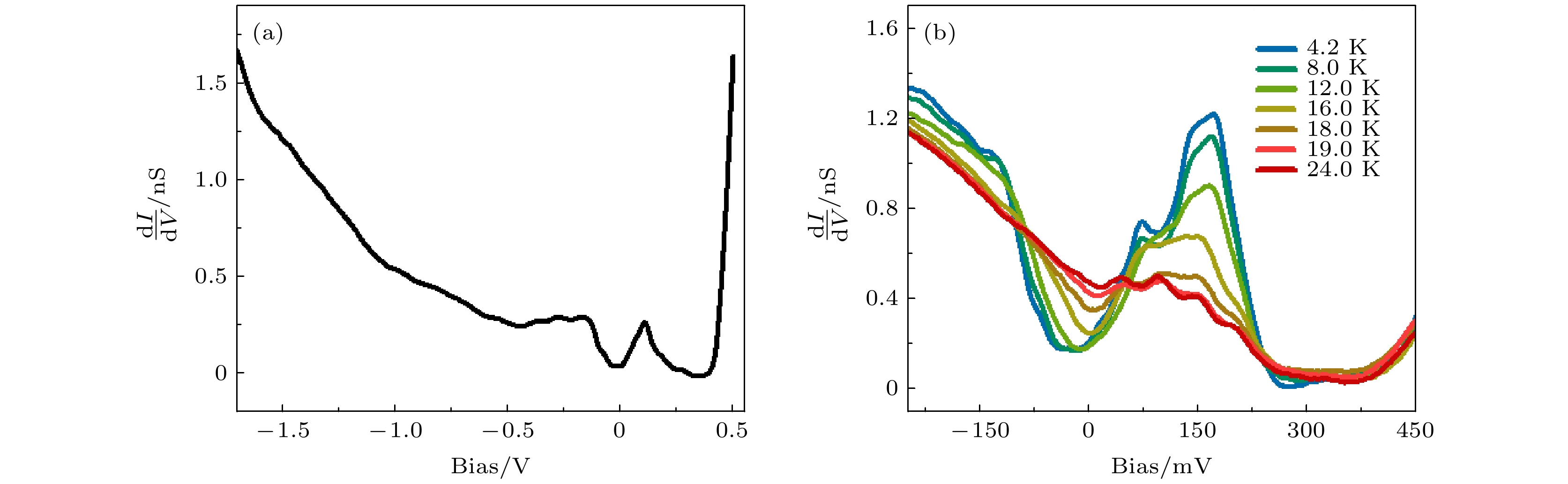 图 3 条纹面上的STS (a) 大能量范围的STS, 采谱条件为Vs = –1.7 V, I = 1 nA, 调制电压为10 mV; (b) 不同温度的STS, 采谱条件为Vs = –250 mV, I = 200 pA, 调制电压为5 mV
Figure3. STS on stripe surface: (a) Large energy range STS, where the spectrum is taken at Vs = –1.7 V, I = 1 nA with modulation 10 mV; (b) STS taken at different temperatures, where the spectra are taken at Vs = –250 mV, I = 200 pA with modulation 5 mV.
在确定条纹面的情况后, 可以进一步讨论迷宫面的结构特征. 在少数台阶内边缘附近(即靠近相邻更高台阶的区域), 可以观测到如图1(e)所示的迷宫结构, 其尺度通常小于20 nm. 图4(a)是迷宫面的原子分辨形貌图. 可以看到迷宫面没有显著的空洞缺陷, 亮条纹由单原子链组成, 原子链在nm尺度发生方向的改变, 在每个转折点亮条纹方向改变120°.
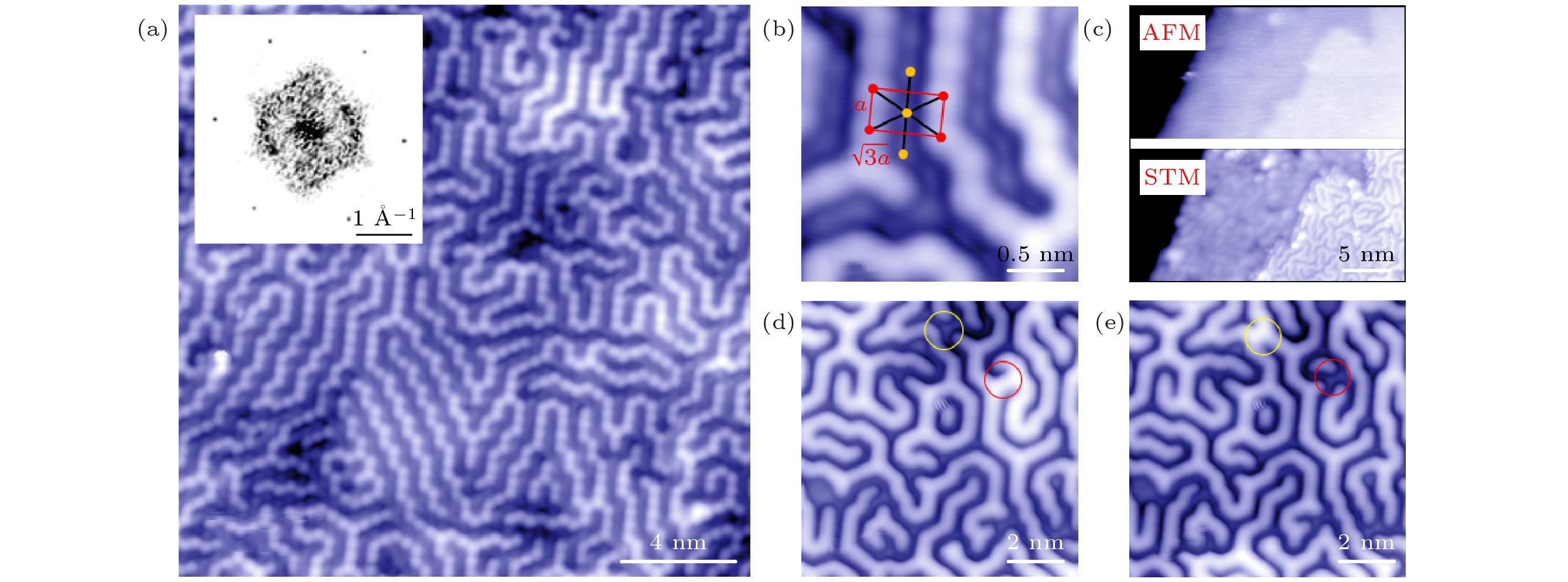 图 4 迷宫面的结构 (a) 迷宫面的原子分辨图 (Vs = 10 mV, I = 100 pA), 插图是相应的FFT图; (b) 小范围的原子分辨STM形貌图 (Vs = 10 mV, I = 100 pA), 暗条纹中可以看到清晰的原子, 原子位置图中用黄球标示; (c)迷宫面和条纹面台阶的AFM (上图)和STM (下图)形貌图, 图中左侧暗区为下层台面, 中部为条纹面, 最右侧为迷宫面, AFM/STM观测的台阶高度为1.1 ?/1.3 ?; (d), (e)迷宫面在电压脉冲下的不稳定性, 在(d)中红色圆圈内施加400 mV的电压脉冲, 表面原子排布变为(e)图所示, 其中黄圈位置的原子由暗变亮, 红圈位置的原子由亮变暗
Figure4. Structure of the maze-like surface. (a) Atomic resolved STM image of maze-like surface (Vs = 10 mV, I = 100 pA), with corresponding FFT image inserted. (b) Small scale atomic resolved STM topography (Vs = 10 mV, I = 100 pA), atoms in the dark stripes, which are marked by yellow dots, are clearly visible. (c) AFM (up panel) and STM (down panel) topography of the step coexisting of maze (right) and stripe (middle) surface. Step height from AFM (STM) is 1.1 ? (1.3 ?). (d), (e) Surface topography evolution under a voltage pulse showing the metastability of the maze-like pattern. A 400 mV voltage pulse is applied in the red circle of panel (d), leading to a rearrangement of atoms in both red and yellow circles from panel (d) to panel (e).
图4(a)中左上角的插图是形貌图对应的FFT, 图中外围6个清晰的点与布拉格点一致, 这表明亮条纹中的原子位于六角格子上. 在更高分辨的原子像(如图4(b))中, 观测到链内原子间距为晶格常数a, 平直亮条纹的间距为

台阶高度是分析不同原子面的重要参数. 但STM所测的表观高度容易受费米能附近的局域态密度影响, 而AFM形貌更接近原子实的实际位置[27]. 图4(c)是STM和AFM在同一台阶区域的形貌图, STM测得迷宫面高出条纹面的表观高度差(1.3 ?)与AFM的观测结果(1.1 ?)基本一致, 这表明STM表观高度差比较真实地反映了原子实的位置. 迷宫面的原子不可能来自比Eu更矮的原子层. 若来自Eu以上的As原子层, 意味着As—In共价键发生断裂, 这在能量上不支持, 而且此处断键应产生丰富的台阶高度差, 与实验观测不符. 一种更合理的情形是, 同一层的Eu原子发生c方向的偏离, 形成迷宫状的翘曲结构.
迷宫面原子这种高低分布的构型并不稳定, 微小的电压脉冲可以改变迷宫面的局部原子排布. 图4(d) 和图4(e) 是400 mV电压脉冲在红圈位置作用前后, 迷宫面的形貌变化, 红圈处条纹由连通变成断点, 有趣的是, 在距离针尖2 nm远的黄圈处, 条纹形状由中断变成连通. 这个过程中, 亮暗原子的个数没有发生变化. 针尖在迷宫面扫图时, 当偏压大于500 mV, 会持续改变迷宫面的形貌. 对微弱电场的敏感表明迷宫面结构不稳定, 原子容易被针尖操纵. 在Si (111)表面沉积金属原子的实验中也观测到了类似的现象[28]. 需要指出, 现有的观测结果, 并不能完全确定迷宫面的结构起源.
类似EuIn2As2中迷宫面的特征, 在很多表面沉积实验中都有报道, 如C60/Cu(111) 的迷宫状图案[29], Sn(1–x)-Six/Si(111) 中的马赛克图案[30]. 在六角格子的系统中, 自旋阻挫是一个广为人知的现象[31,32], C60/Cu(111), Sn(1–x)-Six/Si(111) 体系中所观察到的迷宫/马赛克结构被认为是一种阻挫效应, 利用蒙特卡罗模拟, 二维六角格子上的反铁磁伊辛模型能很好地复现实验结果[29,30]. 这些结果为分析EuIn2As2的迷宫面成因提供了线索, EuIn2As2可能是研究二维六角格子上反铁磁伊辛模型的原子级实验平台.
感谢中国科学院物理研究所翁红明研究员、德国马克斯-普朗克研究所徐远峰博士对材料拓扑性质的讨论, 感谢中国科学院物理研究所方辰研究员、周毅研究员对迷宫面结构的讨论, 感谢中国科学院大学张余洋副教授关于样品解理位置的讨论.
