Fund Project:Project supported by the National Natural Science Foundation of China (Grant No. 60976070)
Received Date:29 December 2020
Accepted Date:17 April 2021
Available Online:07 June 2021
Published Online:05 September 2021
Abstract:This paper studies the changes in electronic transport properties caused by InGaN as an AlGaN/GaN insertion layer, and considers the effects of the spontaneous polarization and piezoelectric polarization of AlGaN and InGaN barrier layers on the surface density of polarized charge, and the concentration of two-dimensional electron gas (2DEG) in AlxGa1–xN/InyGa1–yN/GaN double heterojunction high-electron-mobility transistor. The InGaN thickness and interface roughness scattering, random dipole scattering and polar optical phonons under different In molar compositions are analyzed. The calculation results show that the interface roughness scattering and random dipole scattering have an important influence on the electron transport properties of the double heterojunction AlxGa1–xN/InyGa1–yN/GaN, and the polar optical phonon scattering has the weakest influence; 2DEG concentration, the strength of interface roughness scattering, random dipole scattering and polar optical phonon scattering are determined by the thickness of the InGaN barrier layer and the molar composition of In. This paper takes 2DEG in the AlxGa1–xN/InyGa1–yN/GaN double heterojunction as the research object, considering the barrier layer of finite thickness, taking into account the spontaneous polarization effect and piezoelectric polarization effect of each layer, and giving AlxGa1–xN/GaN 2DEG characteristics in the InyGa1–yN/GaN double heterostructure, discussing the scattering of 2DEG concentration and interface roughness by changing the In molar composition and the thickness of the InGaN barrier layer under the same Al molar composition and the thickness of the AlGaN barrier layer, Random dipole scattering and polar optical phonon scattering. The results of the present study are of great significance in controlling the 2DEG concentration in the AlxGa1–xN/InyGa1–yN/GaN double heterojunction structure and improving the electron mobility. This paper presents the analytical expression of 2DEG concentration ns in AlxGa1–xN/InyGa1–yN/ GaN double heterostructure. The effects of the thickness of the InGaN insertion layer and the molar composition of indium on the 2DEG concentration, interface roughness scattering, random dipole scattering and total mobility are studied. According to the theoretical calculation results, on condition that the physical properties of the AlGaN barrier layer remain unchanged, choosing the appropriate InGaN barrier layer thickness and In molar composition concentration can better control the 2DEG concentration and carrier mobility. These results are beneficial to widely using the double heterojunction AlxGa1–xN/InyGa1–yN/GaN in actual nitride based semiconductor devices. Keywords:two-dimensional electron gases density/ interface roughness scattering/ random dipole scattering/ polar optical phonon scattering
表1AlN, InN, GaN, AlxGa1–xN和InyGa1–yN的各项物理参数(300 K)[17] Table1.Physical parameters of AlN, InN, GaN, AlxGa1–xN and InyGa1–yN[17].
$\begin{split} & {P_{{\rm{PE}}}}\left({{\rm{A}}{{\rm{l}}_x}{\rm{G}}{{\rm{a}}_{1 - x}}{\rm{N}}} \right) = {P_{{\rm{PE}}}}\left( x \right) \\ =\; & 2\frac{{{a_{{\rm{GaN}}}} \!-\! a\left( x \right)}}{{a\left( x \right)}}\left[ {{e_{31}}\left( x \right)\!-\!{e_{33}}\left( x \right)\frac{{{C_{13}}\left( x \right)}}{{{C_{33}}\left( x \right)}}} \right],\end{split}$
$\begin{split} & {P_{{\rm{PE}}}}\left( {{\rm{I}}{{\rm{n}}_y}{\rm{G}}{{\rm{a}}_{1 - y}}{\rm{N}}} \right) = {P_{{\rm{PE}}}}\left( y \right)\\ =\; & 2\frac{{{a_{{\rm{GaN}}}} - a\left( y \right)}}{{a\left( y \right)}}\left[ {{e_{31}}\left( y \right) - {e_{33}}\left( y \right)\frac{{{C_{13}}\left( y \right)}}{{{C_{33}}\left( y \right)}}} \right].\end{split}$
3.计算结果与分析对于半导体异质结AlxGa1–xN/InyGa1–yN/GaN的输运性质的研究, 本文从下面几个方面进行讨论: InyGa1–yN势垒层的厚度和2DEG浓度的关系曲线如图3所示. 图中的实验数据点是In摩尔组分含量为0.1时得到的实验数据, 由此可知, 理论计算结果与实验数据基本一致[26-28]. 插入InyGa1–yN层会使沟道层中2DEG浓度升高, 但In摩尔组分的增加会在一定程度上提高2DEG的浓度: In摩尔组分含量越高, 2DEG浓度随InGaN势垒层厚度的升高越快, 且当InGaN势垒层的厚度处于区间0—5 nm时, 2DEG浓度保持在相对较高的水平. 图 3 在不同In摩尔组分下, InGaN势垒层厚度和二维电子气浓度的关系 Figure3. The relationship between the thickness of InGaN and 2 DEG sheet density under different In mole fraction.
InGaN势垒层厚度和粗糙度散射迁移率之间的关系如图4所示. 界面粗糙度散射限制的迁移率与2DEG浓度的值成反比. 图中实验数据点是In摩尔组分含量为0.15时的实验数据[29,30], 可以看出与理论计算得出的结果相对更为接近, 因此本文中采用理论计算的方法是可行的. 图 4 在不同In摩尔组分下, InGaN势垒层厚度与界面粗糙度散射迁移率之间的关系 Figure4. The relationship between the thickness of InGaN and mobility limited by interface roughness scattering under different In mole fraction.
InGaN势垒层厚度和偶极子散射迁移率之间的关系如图5所示, 图中的实验数据点代表的是In摩尔组分含量为0.15的实验数据[31], 本文计算结果与现存的实验数据存在一定误差, 理论模型需要进行进一步细化, 减小误差. 误差可能来自计算屏蔽电位的过程中质心距离和正负电荷中心距离的取值. InGaN势垒层厚度的增加会提升随机偶极散射对载流子迁移率的影响, 且In摩尔组分越大, 随机偶极散射限制的迁移率升高越快, 证明In摩尔组分含量降低会大大降低随机偶极散射对载流子迁移率的影响. 图 5 在不同In摩尔组分下, InGaN势垒层厚度与随机偶极散射的迁移率之间的关系 Figure5. The relationship between the thickness of InGaN and mobility limited by random dipole scattering under different In mole fraction.
极性光学声子散射迁移率和InGaN势垒层厚度的关系如图6所示, 图中实验数据点[31]是In摩尔组分含量为0.05时的实验数据, 与理论计算结果较为接近, 误差在允许范围内. 对于InGaN沟道层而言, 随着InGaN势垒层厚度的增加, In组分含量越低迁移率下降越慢. 图 6 极性光学声子散射迁移率和InGaN势垒层厚度的关系 Figure6. The relationship between the thickness of InGaN and polar optical phonon scattering.
综上所述, 在完成不同散射种类影响下迁移率的研究的同时, 我们需要考虑总迁移率与InGaN插入层厚度的关系曲线. 以Al摩尔组分为0.2, In摩尔组分为0.05为例, 无InGaN插入层时总迁移率只有7395.748 cm2·V–1·s–1, 此时限制迁移率的主要散射机制是界面粗糙度散射, 随着InGaN势垒层厚度增加, 限制迁移率的主要散射机制已经由界面粗糙度散射转变为随机偶极散射. 倘若继续增加InGaN势垒层的厚度至 InGaN势垒层厚度大于5 nm之后, 2DEG浓度会保持在某一取值范围稳定不变. 图7给出了在不同In摩尔组分下, 总迁移率和InGaN势垒层厚度的关系. 当In摩尔组分为0.05, 0.10和0.15时, 起初总迁移率也会由于界面粗糙度散射迁移率的降低而明显增大, 但达到极值之后, 随着InGaN势垒层厚度的增加, 迁移率降低并没有In摩尔组分为0.15时明显. 图 7 在不同In摩尔组分下, 总迁移率和InGaN势垒层厚度的关系 Figure7. The relationship between the thickness of InGaN and total mobility under different In mole fraction.
 图 1 AlxGa1–xN/InyGa1–yN/GaN异质结结构图
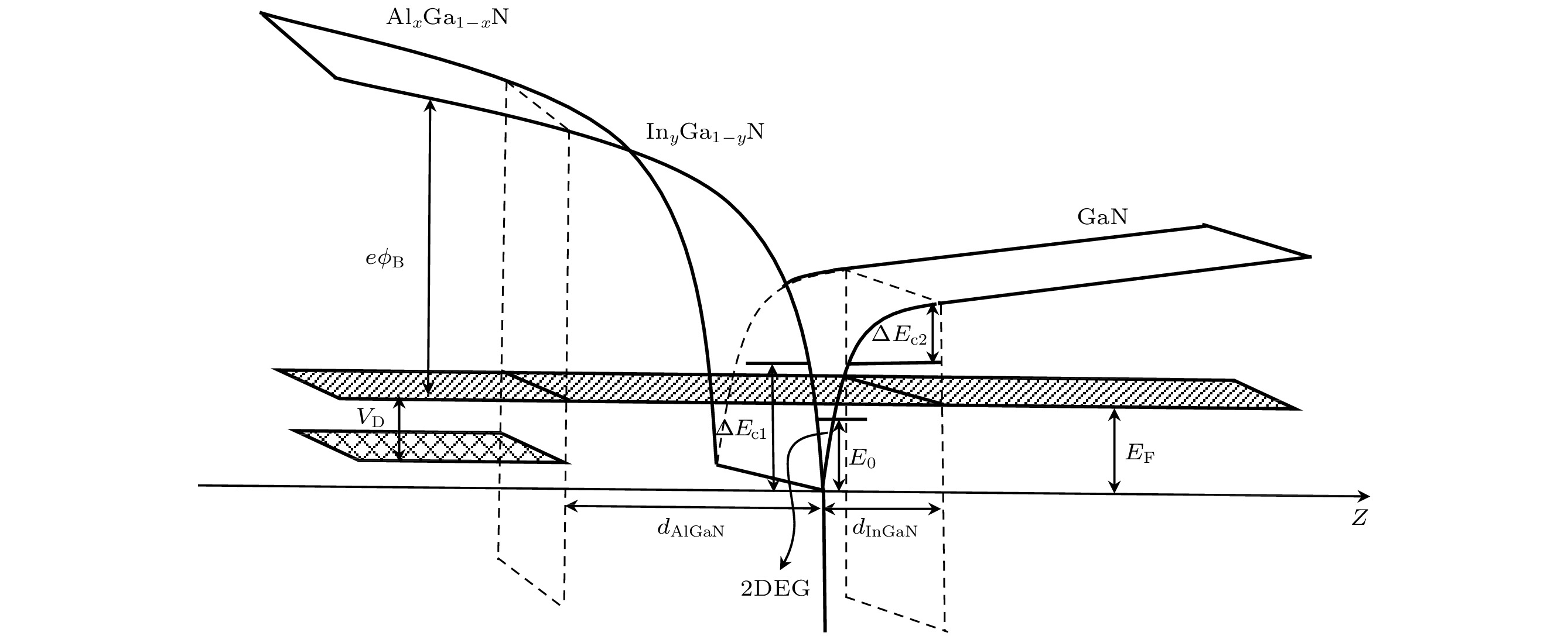 图 2 AlxGa1–xN/InyGa1–yN/GaN异质结导带剖面示意图


 图 3 在不同In摩尔组分下, InGaN势垒层厚度和二维电子气浓度的关系
 图 4 在不同In摩尔组分下, InGaN势垒层厚度与界面粗糙度散射迁移率之间的关系
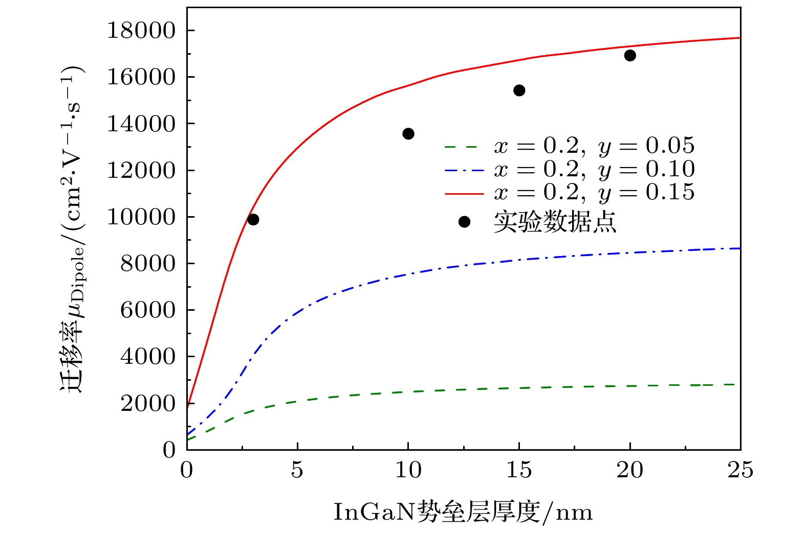 图 5 在不同In摩尔组分下, InGaN势垒层厚度与随机偶极散射的迁移率之间的关系
 图 6 极性光学声子散射迁移率和InGaN势垒层厚度的关系
 图 7 在不同In摩尔组分下, 总迁移率和InGaN势垒层厚度的关系