1.School of Physics and Optoelectronic, Xiangtan University, Xiangtan 411105, China 2.School of Mathematics and Computational Science, Xiangtan University, Xiangtan 411105, China 3.Chongqing Institute of Green and Intelligent Technology, Chinese Academy of Sciences, Chongqing 400714, China
Fund Project:Project supported by the Natural Science Foundation of Hunan Province, China (Grant No. 2019JJ40280), the Research and Development Project of Key Field of Hunan Province, China (Grant No. 2019GK2101), the Innovation Project of Degree and Postgraduate of Hunan Province, China (Grant Nos. 2020JGYB097,?2020JGYB098), and the Innovative Research Program for College Students of Hunan Province, China (Grant No. S201910530020).
Received Date:16 February 2021
Accepted Date:30 March 2021
Available Online:07 June 2021
Published Online:05 September 2021
Abstract:As a type of two-dimensional (2D) semiconductor material, 2D germanium selenide (GeSe) exhibits excellent optoelectronic properties, and has potential applications in optoelectronic devices. The GeSe is a layered material with weak van der Waals interaction. Because of the high brittleness of GeSe, it is not easy to obtain 2D GeSe samples only by mechanical peeling technique. In order to obtain a thinner GeSe sheet, we use heat treatment to thin the bulk GeSe at a high temperature in vacuum. The GeSe samples obtained by mechanical peeling are placed in a tubular furnace with a pressure of 5 × 10⁻⁴ Pa for high temperature heating and thinning. In order to explore the better thinning effect, we set four temperatures to be at 320, 330, 340 and 350 ℃, respectively. After high temperature thinning, the samples are characterized and observed by atomic force microscope (AFM), scanning electron microscope (SEM), Raman spectrometer and photoluminescence (PL) spectrometer. From the above experiments, the GeSe nanosheet with a thickness of about 5 nm is prepared by mechanical peeling and high temperature thinning technology. Then, the electrical conductivities of GeSe nanosheets in oxygen (O2) and butane (C4H10) with different concentrations are evaluated by our designed experimental device. The results show that with the increase of oxygen concentration, the electrical conductivity of GeSe nanosheets increases. When the GeSe nanosheet is in butane gas, its conductivity under the same voltage decreases with the increase of the concentration of butane gas. In order to further analyze the mechanism of gas adsorption on GeSe nanosheets, we carry out the first-principles calculations. Our calculation results show that the adsorption energy of GeSe nanosheets for oxygen and butane is –4.555 eV and –4.865 eV, respectively. It is shown that both adsorption systems have a certain stability. The adsorption energy of C4H10 is smaller than that of O2, which corresponds to the smaller layer spacing of C4H10 than that of O2 on GeSe surface. From Bader analysis, it is shown that 0.262e is transferred from the surface of GeSe nanosheet to O2 molecule, which is much larger than 0.022e transferred from GeSe to C4H10 molecule. It can be inferred that the bond formed between GeSe and O2 molecule is covalent bond, while GeSe adsorption C4H10 is very fragile hydrogen bond adsorption. In an ideal condition (single atomic GeSe layer, no Se vacancy, and the device preparation process is vacuum), our calculation results show that C4H10 still has a weak ability to obtain electrons from the GeSe nanosheet. However, the complex conditions such as the actual layer thickness, the appearance of Se vacancy and the adsorption of O2 molecules on the surface leads to the difference between the experimental results and the theoretical calculations, which can be attributed to the adsorption of O2 molecules on the GeSe surface from the air during the processing of GeSe thinning and device fabrication. Owing to the high density of Se vacancies in the thin film, the high density of O2 adsorption is caused. Thus, butane gas is easy to lose electrons on the GeSe surface due to the O2 adsorption. In other words, electrons are transferred from butane gas molecules to the surface of GeSe film and neutralized with holes, which reduces the concentration of carriers and the concentration of holes in GeSe film, thus reducing the conductivity. Our research will contribute to the application of GeSe nanosheets in optoelectronic devices at the atmosphere of oxygen and butane. Keywords:GeSe nanosheet/ electrical conductance/ gas adsorption/ first-principle
涉及的计算研究采用基于密度泛函理论(density functional theory, DFT)的第一性原理方法, 使用VASP软件包[28]开展二维GeSe吸附氧气和丁烷气体计算. 电子-电子交换关联作用运用广义梯度近似(GGA)[29,30]中的PBE赝势[31]. 电子-离子之间的交换电位相互作用为PAW方法[32]. 能量的计算精度为1.0 × 10⁻⁵ eV, 平面波截断能为450 eV. 布里渊区积分基于Monkhorst-Pack方法[33], K点设置为9 × 9 × 1. 每个原子上的作用力收敛标准为小于0.01 eV/?. 范德瓦耳斯力 (vdW) 修正采用DFT-D3函数[34], 来描述气体分子与单层GeSe超胞之间微弱的范德瓦耳斯力作用. 图3(a)给出了GeSe单胞结构的侧视图和俯视图, 其中Ge—Se键长为2.53 ?. 图3(b)为其能带图, 带隙值为1.12 eV. 晶格常数为a0 = 4.25 ?, b0 = 3.99 ?, 沿Z轴方向20 ?的真空层确保相邻吸附体系之间无相互作用. 图3(d)和图3(e)分别为吸附O2的侧视图与俯视图以及吸附C4H10的侧视图与俯视图. 图 3 (a) GeSe单胞的结构; (b) GeSe单层的能带结构; (c) GeSe上吸附位点G点, S点, C点和B点的示意图; (d) GeSe吸附氧气最稳定的吸附结构示意图(侧视图与俯视图); (e) GeSe吸附丁烷最稳定的吸附结构示意图(侧视图与俯视图). 黄色, 绿色, 红色, 黑色和白色的球分别代表着Se, Ge, O, C和H原子 Figure3. (a) Optimized structure of GeSe monolayer; (b) band structures of GeSe monolayer; (c) considered positions for gas molecules adsorption: G site, S site, C site and B site on GeSe monolayer, respectively; (d) obtained stable adsorption configuration (side and top view) for O2 on GeSe monolayer; (e) obtained stable adsorption configuration (side and top view) for C4H10 on GeSe monolayer. The yellow, green, red, black and white balls denote Se, Ge, O, C and H atoms, respectively.
表1吸附能(Ea), GeSe与气体分子之间的电荷转移量(ρ)以及它们之间的最近距离(d ) Table1.Calculated adsorption energy (Ea), the charge transfer (ρ) between gas molecules and monolayer GeSe, and the nearest distance (d ) between them.
图5为GeSe吸附体系的差分电荷密度图以及电子局域函数图. 图5(a)为GeSe吸附氧气的差分电荷密度图, 发现电荷从基底GeSe向O2分子转移. 图5(b)为GeSe吸附丁烷的差分电荷密度图, 发现C4H10气体分子与GeSe之间几乎没有电荷转移. 为了进一步确认Ge原子和氧原子之间的结合方式, 图5(c)和图5(d)分别给出了O2分子和C4H10分子吸附在二维GeSe上的电子局域函数 (ELF)图. ELF图中的局域程度用刻度值来显示, 其值一般在0—1.00之间. 1.0和0.50的取值分别对应体系完全局域化和电子完全离域, 而0则表示电荷密度非常低, 几乎可以忽略不计[35]. 从图5(c)可以看出, O2分子与GeSe基底之间的ELF值为0.2左右, 因此离子键在O2分子与GeSe基底之间形成. 而C4H10分子与与GeSe基底之间的ELF值为0, 说明它们之间仅存在极弱的范德瓦耳斯力相互作用. 图 5 GeSe吸附(a)氧气和(b)丁烷的差分电荷密度图, 等值面分别取0.01和0.0009e/A3. 其中蓝色原子为硒原子, 棕色原子为锗原子, 红色为氧原子, 黑色为碳原子, 粉色为氢原子; 黄色部分表示得到电子, 绿色部分表示失去电子. GeSe吸附(c)氧气和(d)丁烷的电子局域图, 左边是ELF (e/A3) 的参考值 Figure5. Charge density difference for the configurations of (a) O2 and (b) C4H10 on GeSe monolayer. The plotted isosurface is 0.01e/A3 and 0.0009e/A3, respectively. Blue atoms are selenium atoms, brown atoms are germanium atoms, red are oxygen atoms, black are carbon atoms, and pink are hydrogen atoms. In the differential charge density graph, the yellow part indicates the gain of electrons, and the green part indicates the loss of electrons. Electron localization function (ELF) for configurations of (c) O2 and (d) C4H10 adsorbed on GeSe monolayer, respectively. The ELF value is listed at the left side with a unit of e/A3.
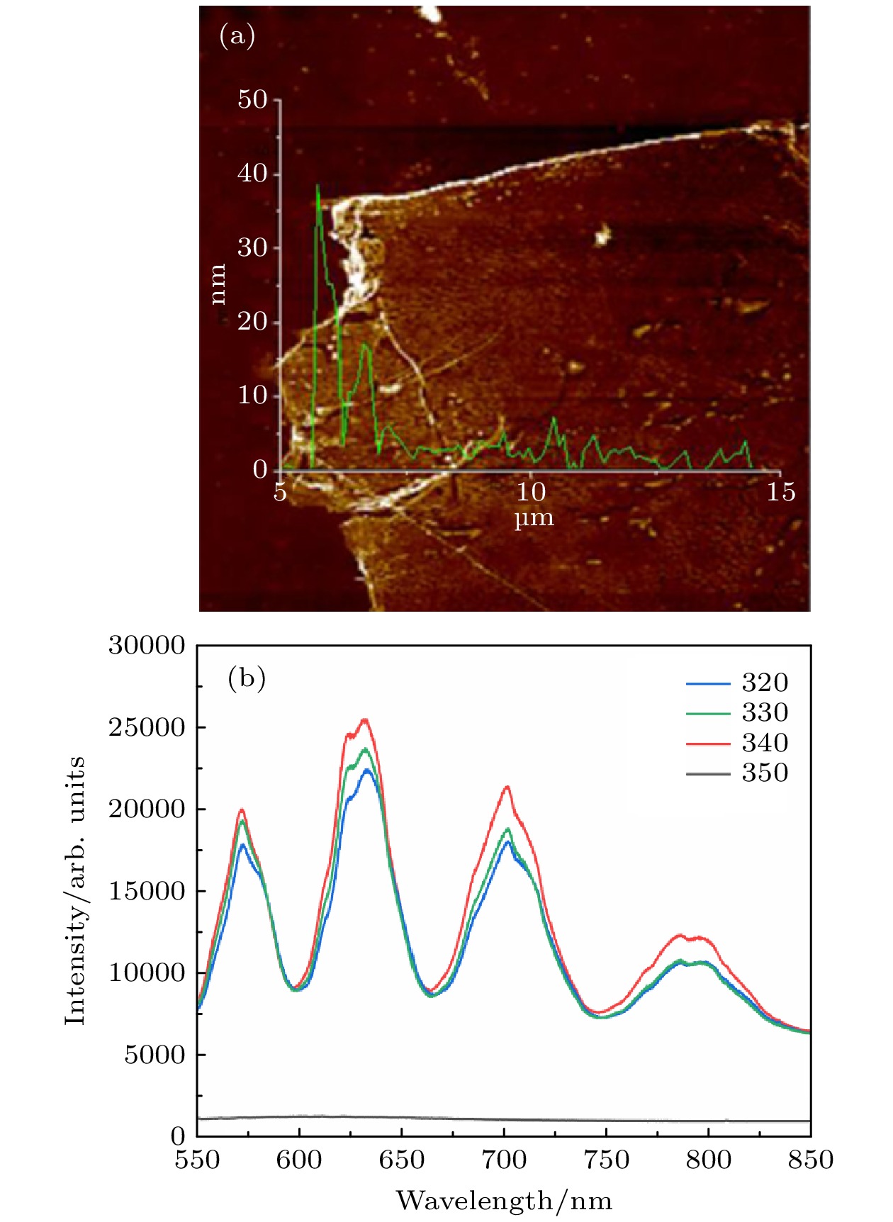 图 1 (a)原子力显微镜表征图 (在图像中插入的绿线显示了减薄后GeSe的厚度); (b)光致发光光谱图
 图 2 自制实验气体腔 (a)原理图; (b)实物图
 图 3 (a) GeSe单胞的结构; (b) GeSe单层的能带结构; (c) GeSe上吸附位点G点, S点, C点和B点的示意图; (d) GeSe吸附氧气最稳定的吸附结构示意图(侧视图与俯视图); (e) GeSe吸附丁烷最稳定的吸附结构示意图(侧视图与俯视图). 黄色, 绿色, 红色, 黑色和白色的球分别代表着Se, Ge, O, C和H原子


 图 4 (a) GeSe纳米片吸附不同浓度的氧气时电压-电流特性曲线; (b) GeSe纳米片吸附不同浓度的丁烷气时电压-电流特性曲线
 图 5 GeSe吸附(a)氧气和(b)丁烷的差分电荷密度图, 等值面分别取0.01和0.0009e/A3. 其中蓝色原子为硒原子, 棕色原子为锗原子, 红色为氧原子, 黑色为碳原子, 粉色为氢原子; 黄色部分表示得到电子, 绿色部分表示失去电子. GeSe吸附(c)氧气和(d)丁烷的电子局域图, 左边是ELF (e/A3) 的参考值