全文HTML
--> --> -->二维生物传感器通常是利用二维材料作为信号转换元件来传递生物信号的器件. 相较于传统的生物传感器, 二维材料制备的传感器在电子转移效率、比表面积和掺杂灵敏度方面都远高于传统金属材料. 这也使得二维材料制备的电化学[17,18]、晶体管[19-25]和荧光(FRET)传感器[26-30]的灵敏度远高于传统金属和半导体制备的电化学、晶体管和荧光传感器.
目前, 二维生物传感器的性能已经超过传统生物传感器, 二维材料掺杂和传感界面设计方法仍在不断发展, 使得传感性能进一步提升. 将N, B, S等原子精准地掺杂到二维材料表面, 有效增加材料的电子态密度和活性, 从而大幅提升二维电化学传感器的灵敏度. 除了对二维材料精准原子掺杂以外, 在二维材料表面精准地构筑分子级生物探针可以有效拓宽传感器的检测物范围. 常见的生物探针有酶、抗体、核酸适配体等. 这些分子级生物探针往往拥有强特异性和高灵敏度等特点. 但各自也有一些不足, 比如酶虽然特异性强, 但其可检测物质的范围较窄; 抗体传感器虽然特异性强、检测范围较广, 但其生产成本高、各批次均一性较差; 核酸适配体作为一种可人工合成的新型生物探针, 其特异性强、检测范围广、各批次间均一性好, 但是核酸适配体筛选方法的专利授权费用高昂, 限制其大规模商业化开发. 除以上探针可用于构筑生物传感界面外, 一些生物和化学小分子也被用于精准地修饰传感界面, 用以精确调控被检测物质的相关化学反应, 实现对一些寿命很短的化学分子进行相关检测.
根据以上几种生物界面的修饰方法来看, 对二维生物传感界面进行精准的分子和原子构筑, 精确调控了传感过程中的相互作用和化学反应, 进一步有效提升器件灵敏度和检测物范围. 开发新的原子级界面构筑方法, 对于高性能生物传感器的研究至关重要. 本文将综述在二维生物传感界面精准原子构筑领域的最新进展, 并探讨其存在的问题和未来发展方向.
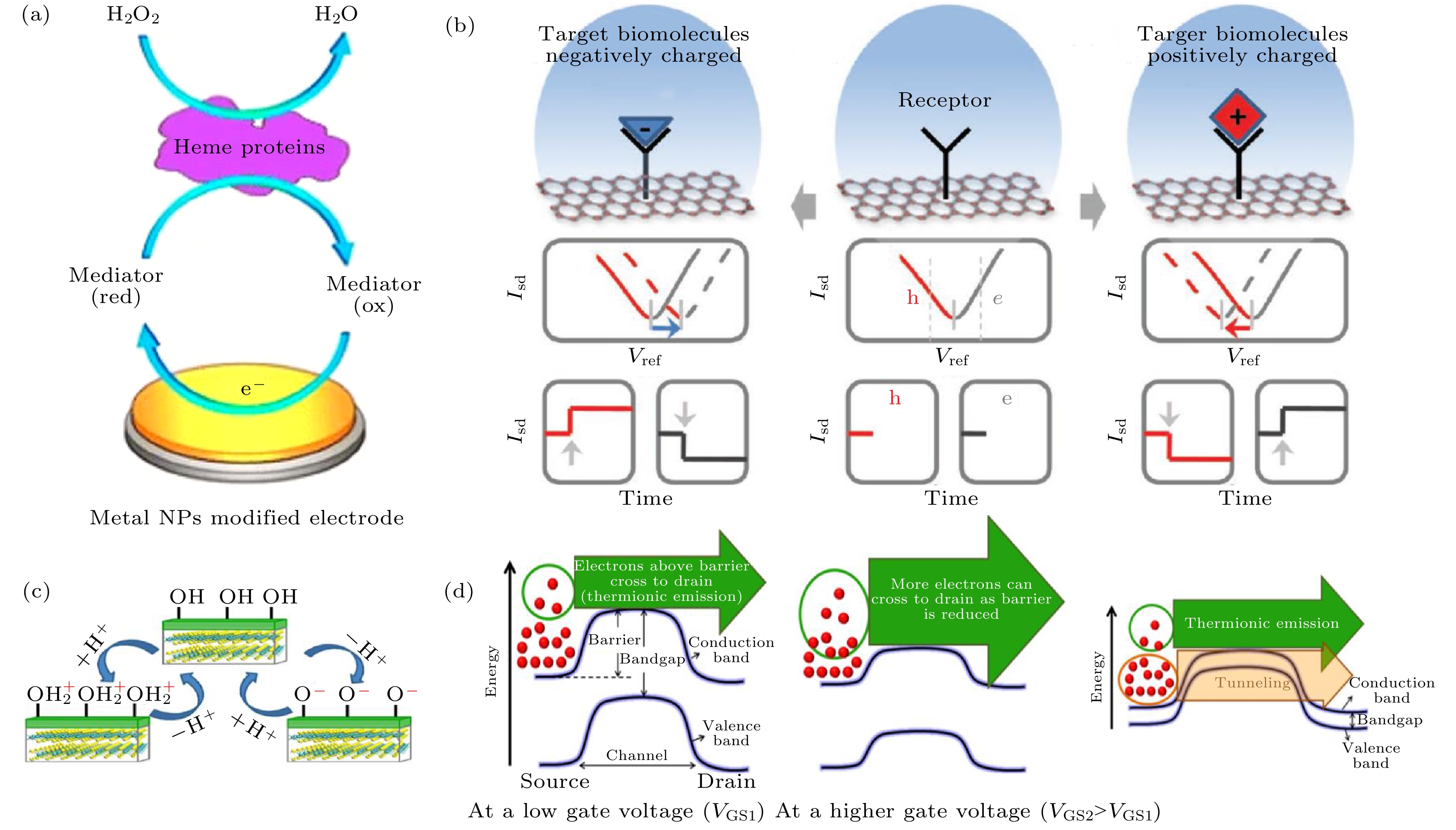 图 1 (a)电化学传感过程示意图[31]; (b)石墨烯场效应晶体管利用场效应检测带电分子传感过程示意图[10]; (c) 硫化钼晶体管检测pH值时吸附离子过程示意图; (d)吸附离子前后, 硫化钼能带示意图; 吸附离子前, 半导体与电极之间形成肖特基势垒, 能量较低的电子无法穿越势垒; 吸附离子后, 相当于给晶体管增加了栅极电压, 使得势垒降低, 能量较低的电子也可以穿越势垒; 除此之外, 还有少部分电子可以以隧穿形式穿过势垒[38]
Figure1. (a) Schematic of sensing mechanism of electrochemical sensors[31]. (b) Schematic of sensing mechanism of graphene transistor[10]. (c) Illustration of the principle of pH sensing. At lower pH (higher concentration of H+ ions), the OH group on the dielectric surface gets protonated to form

2
2.1.二维材料掺杂及其生物传感应用
原子掺杂可以有效调节二维材料的电学性质和表面化学势, 比如氮(N)掺石墨烯可以有效增加材料的自由载流子密度, 以及导热导电能力[52,53]. N掺杂石墨烯具有高的电子态密度, 可以辅助电化学中的还原反应, 提高电化学生物传感器的灵敏度.如图2所示, 一个氮掺杂的石墨烯电极可用于葡萄糖氧化酶检测. 葡萄糖氧化酶能够催化葡萄糖与氧气发生氧化反应, 产生葡萄糖酸和过氧化氢. 氮掺杂石墨烯的高电子态密度使其表面的过氧化氢更容易发生还原反应, 从而可以得到更大的还原电流信号, 有效提升了传感器的灵敏度. 硼原子掺杂的石墨烯也展示了优异的电催化活性, 基于硼掺杂的石墨烯被广泛用于电化学检测, 比如可以检测对苯二酚[54]、过氧化氢[55]、鸟嘌呤[56]等. 此外, 硫原子掺杂的石墨烯可以有效增加石墨烯的表面积, 从而提升传感器性能[57]. 在二维材料表面进行元素掺杂, 实现了电化学传感界面的精准原子构筑, 是一种有效改善电化学传感器性能的方法.
 图 2 氮掺杂石墨烯用于葡萄糖氧化酶检测 (a) N掺杂石墨烯示意图, 灰色为碳原子, 蓝色为氮原子, 白色为氢原子; (b) 分别在氮掺杂石墨烯和石墨烯上的葡萄糖氧化酶的循环伏安曲线, 溶液环境为氮气饱和的0.1 mol/L磷酸盐(PBS)溶液; (c) 分别固定在光滑碳电极、石墨烯电极和氮掺杂电极上的葡萄糖氧化酶电流-时间曲线, 电压为–0.15 V, 溶液环境为0.1 mol PBS的溶液(pH值为7.0), 其中葡萄糖每次添加量为0.1 mmol/L[1]
Figure2. (a) Schematic representation of N-doped graphene. Gray for the carbon atom, blue for the nitrogen atom, and white for the hydrogen atom. (b) Cyclic voltammograms of GOx immobilized on N-doped graphene electrode (solid line) and graphene electrode (dashed line) in N2-saturated 0.1 mol/L phosphate buffered saline (PBS) solution (pH 7.0). Dotted line is for the background. Scan rate is 0.05 V/s. (c) Current-time curves for GOx immobilized on GCE, graphene electrode, and N-doped graphene electrode at –0.15 V in 0.1 mol/L PBS (pH 7.0) with successive addition of 0.1 mmol/L glucose[1].
2
2.2.金属纳米颗粒修饰生物传感界面
金属纳米颗粒修饰二维材料可以有效提升材料的导电性和电子转移能力, 从而提升电极的活性. 如图3(a)—(d)所示, Su等[58]用金纳米颗粒修饰硫化钼, 增加了硫化钼的导电性和纳米结构的稳定性, 实现了对多巴胺的高灵敏度探测(探测极限为80 nmol/L). 铜纳米颗粒也被用于硫化钼纳米片的修饰, 成功在碱性环境中实现了对葡萄糖的检测[59]. 此外, 半金属的石墨烯也常被用于修饰硫化钼纳米片, 石墨烯不仅可以增加硫化钼的导电性, 还可以提供一个多孔结构来提高其催化能力, 如图3(e)和图3(f)所示[60]. 石墨烯修饰的硫化钨也展示了较强的活性, 被用于检测邻苯二酚、间苯二酚和对苯二酚等[54]. 在二维生物传感界面精准构筑金属纳米颗粒可以提升材料的导电性、催化效率, 是一种改善电化学类器件的有效方法.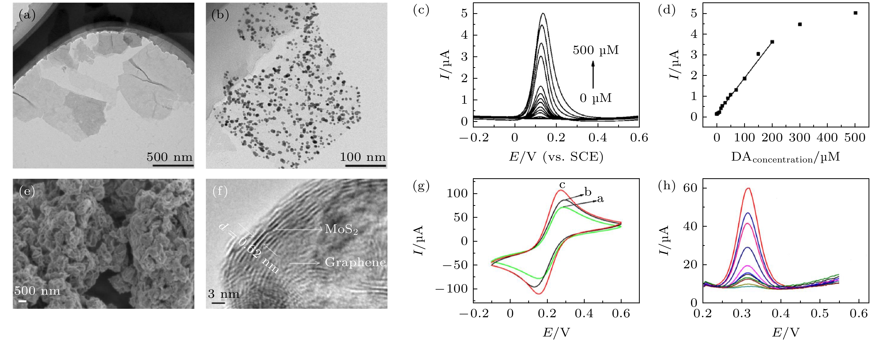 图 3 (a) 硫化钼的隧道电子显微镜(TEM)图; (b) 金纳米颗粒在硫化钼上的TEM图; (c) 基于金纳米颗粒@硫化钼纳米片修饰的光滑碳电极测试不同浓度多巴胺的循环伏安曲线(1 μM = 1 μmol/L); (d) 氧化峰电流和多巴胺浓度的关系曲线[60]; (e) 石墨烯-硫化钼混合物的扫描电子显微镜(SEM)图; (f) 硫化钼-石墨烯高分辨TEM图; (g) 三种不同电极(光滑碳电极、石墨烯在光滑碳电极上、硫化钼-石墨烯在光滑碳电极上)在5 mmol/L
Figure3. Tunneling electron microscope (TEM) images of the (a) MoS2 and (b) AuNPs@MoS2 nanostructures; (c) differential pulse voltammetric curves of different dopamine (DA) concentrations at AuNPs@MoS2/GCE; (d) plot of oxidation peak currents vs. DA concentrations derived from voltammograms of differential pulse voltammetry (DPV)[60]; (e) scanning electron microscope (SEM) images of MoS2-Gr; (f) high-resolution TEM of MoS2-Gr; (g) CVs of GCE, Gr/GCE and MoS2-Gr/GCE in 5 mmol/L

2
2.3.酶修饰生物传感界面
酶是一种高催化效能且特异性强的传感物, 可用于识别一些特定的被酶催化的生物分子. 生物分子与酶的反应产物能有效对石墨烯进行掺杂, 从而可以改变晶体管沟道的跨导, 将被测物浓度转化成电信号. 在多数传感原理中, 都需要生物分子以共价键结合到石墨烯表面, 这会破坏石墨烯的sp2结构和生物分子的折叠结构. 而酶传感器是以静电吸附力附着在石墨烯表面, 很好地避免了共价键对生物分子和石墨烯sp2结构的破坏.如图4(a)和图4(b)所示, 尿素酶以静电力吸附在石墨烯上, 避免了对石墨烯的破坏, 也能高效催化尿素的水解反应. 水解反应的产物会改变溶液的pH值, 从而影响石墨烯晶体管的电流值[61]. 此外, Huang等[62]用葡萄糖氧化酶和谷氨酸脱氢酶修饰石墨烯场效应晶体管, 实现了对葡萄糖和谷氨酸的灵敏检测. 在此工作以后, Kavitha等[63]开发了一款更加灵敏的利用氧化锌纳米颗粒修饰石墨烯薄膜的葡萄糖传感器. 酶除了能用于场效应晶体管修饰之外, 还能修饰在电化学传感器的电极上, 实现高效动态的生物检测, 如图4(c)和图4(d)所示[64].
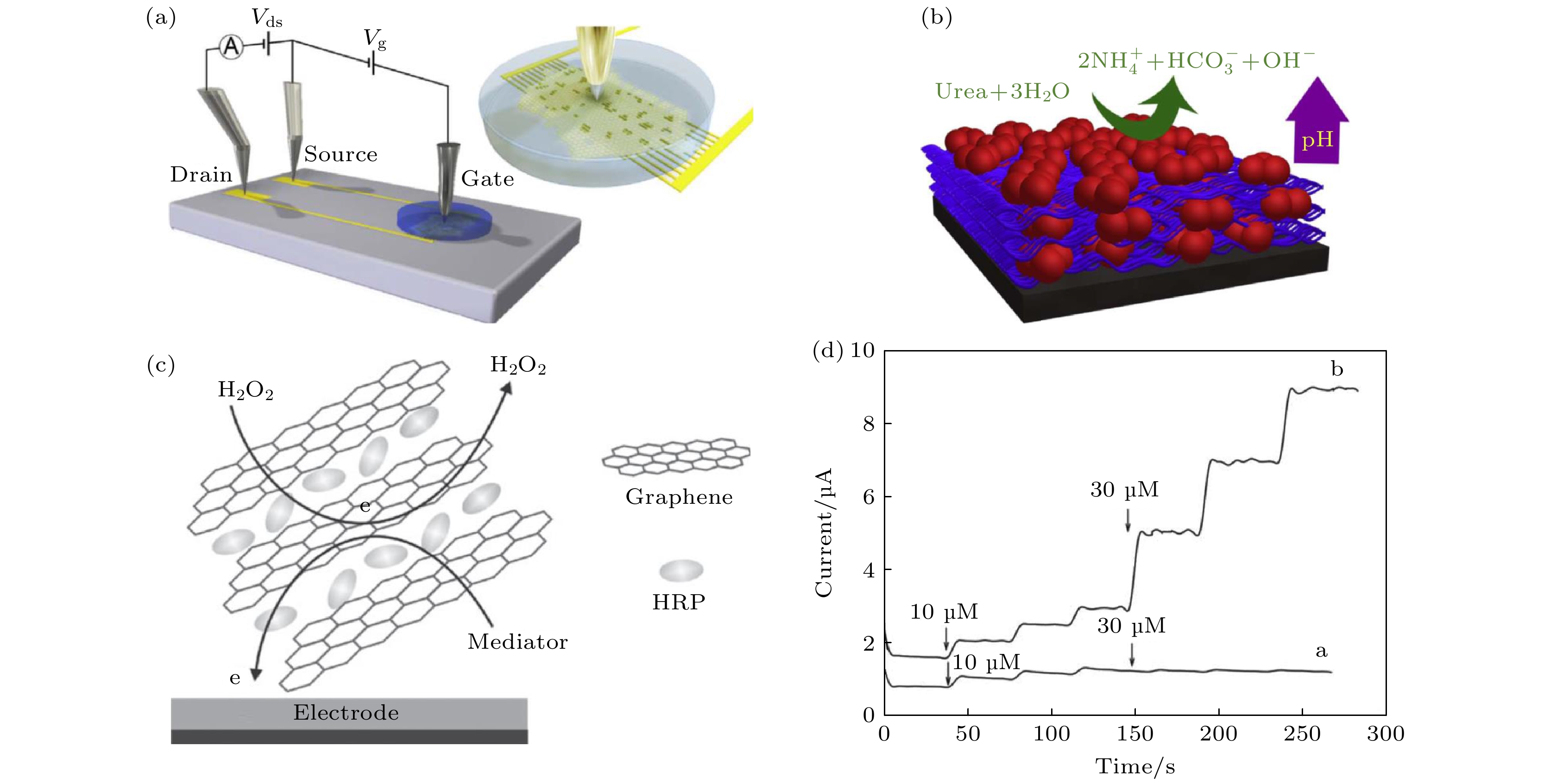 图 4 (a) 液体栅极石墨烯场效应晶体管示意图; (b) 由尿素酶连接的多层石墨烯对尿素催化水解反应的示意图[61]; (c) 自组装辣根过氧化物酶-石墨烯纳米片复合材料示意图; (d)玻碳电极和辣根过氧化物酶-石墨烯纳米片复合电极对过氧化氢溶液的动态电学响应[64]
Figure4. (a) Illustration of the solution gated reduced-graphene-oxide FET and the interdigitated channel; (b) schematic of the urease-polyethylenimine multilayer film and the urease-catalyzed hydrolysis of urea[61]; (c) schematic representation of the self-assembled horseradish peroxidase (HRP)-graphene sheets (GSs) hierarchical bionanocomposites on glass carbon electrode and electron transfer process of the composites on the electrode surface; (d) dynamic amperometric response of the modified electrodes to successive additions of H2O2: SGSs electrode (curve a) and HRP-GSs electrode (curve b) in a stirred 0.1 mol/L PBS (pH 7.0) solution containing 1.0 mmol/L hydroquinone[64].
2
2.4.抗体修饰生物传感界面
抗体是利用其与抗原的氢键来捕获和识别目标分子的, 然后利用场效应将检测物浓度转化为电信号. 相比于酶的传感机制, 抗体的识别范围更广, 可以识别蛋白质、核酸、病毒、小分子化合物等. 因此, 基于抗体修饰的生物传感器也比酶修饰的生物传感器应用更广. 如图5所示, 抗体修饰在硫化钼晶体管的介电层上, 实现了对肿瘤坏死因子α的有效检测[65]. 除硫化钼以外, 抗体也修饰在其他二维材料的晶体管上来检测相关病原体. Mao等[66]利用金纳米颗粒将免疫球蛋白G抗体连接在还原氧化石墨烯晶体管上, 将探测极限提升到2 ng/mL. Chen等[67]用金纳米颗粒将免疫球蛋白G抗体修饰在黑磷晶体管上, 取得了优异的探测极限(10 ng/mL)和响应时间(< 10 s). 抗体和酶传感器都利用哺乳动物细胞生产, 这也造成了其成本高, 各批次差异性较大等特点, 对器件性能标定造成了较大困难. 因此, 实现生物探针的人工合成对于生物传感器大规模商业应用至关重要. 图 5 (a) 硫化钼场效应晶体管生物传感器示意图, 其中功能层用氧化铪和抗体修饰, 用于检测肿瘤坏死因子α (TNF-α); (b) 硫化钼晶体管的光学照片, 沟道长5 μm, 宽6 μm; (c) 集成微流道系统的生物传感器光学照片; (d) 硫化钼晶体管在不同浓度TNF-α下的转移曲线[65]
Figure5. (a) Functionalization of the HfO2 effective layer with antibody receptors and subsequent TNF-α detection; (b) an exemplary MoS2 transistor with channel length (L) and width (W) of 5 μm and 6 μm, respectively; (c) a transistor biosensor integrated with a microfluidic channel system connected with an inlet/outlet tubing kit, which is driven by a motorized syringe pump; (d) transfer characteristics of an exemplary MoS2 transistor sensor measured at various biodetection stages, following the sequence of bare transistor, antibody functionalization, and inputs of TNF-α solutions with concentrations of 60 fmol/L (fM), 300 fmol/L, 600 fmol/L, 3 pmol/L (pM), and 6 pmol/L[65].
2
2.5.DNA及DNA适配体修饰生物传感界面
核酸适配体是利用固相合成技术, 各个批次间差异小, 产品均一性高, 且其生产时间(数小时)也远远小于抗体的生产时间(数天至数月). 此外, 核酸适配体的识别靶点也远大于抗体, 可识别离子、多肽、小分子化合物、蛋白质、核酸、病毒、细菌、细胞和组织等. 所以, 人工筛选的核酸适配体有极好的商业应用前景. DNA适配体有两种机制实现生物信号到电信号传感. 第一种情况: 当目标分子带电时, DNA适配体包裹其靠近石墨烯表面, 会在石墨烯内部感应出与目标分子带电特性相反的电荷, 对石墨烯进行掺杂, 导致其狄拉克点偏移. 第二种情况: 由于DNA适配体独特的二级和三级结构, 当包裹目标分子时, DNA适配体自身的结构发生改变, 成为一个稳定的紧凑结构, 并产生电子丰富的芳香结构, 这种芳香结构与石墨烯直接相互作用形成π—π结构, 电子通过π—π键从DNA适配体直接转移到石墨烯中, 从而改变石墨烯内部载流子浓度密度, 引入n型掺杂, 转移特性曲线左移.适配体结合石墨烯超高的迁移率, 适配体石墨烯FET将会是一个检测范围广、特异性强、灵敏度高、检测极限低的生物传感器件. 最初, Ohno等[8]将免疫球蛋白适配体修饰到石墨烯FET沟道上, 实现了对免疫球蛋白的灵敏检测, 检测极限为0.29 nmol/L. 此后, 一系列放大信号的方法被开发, Kim等[68]将金纳米颗粒修饰在被检测物质(抗原63 5-12)上, 当目标物被适配体捕获后, 金纳米颗粒进一步提升石墨烯沟道导电性, 检测极限被降低到1.2 amol/L, 如图6(a)所示. Gao等[69]提出了利用核酸循环扩增反应提升传感器信噪比的方案, 将检测极限降低到50 amol/L.
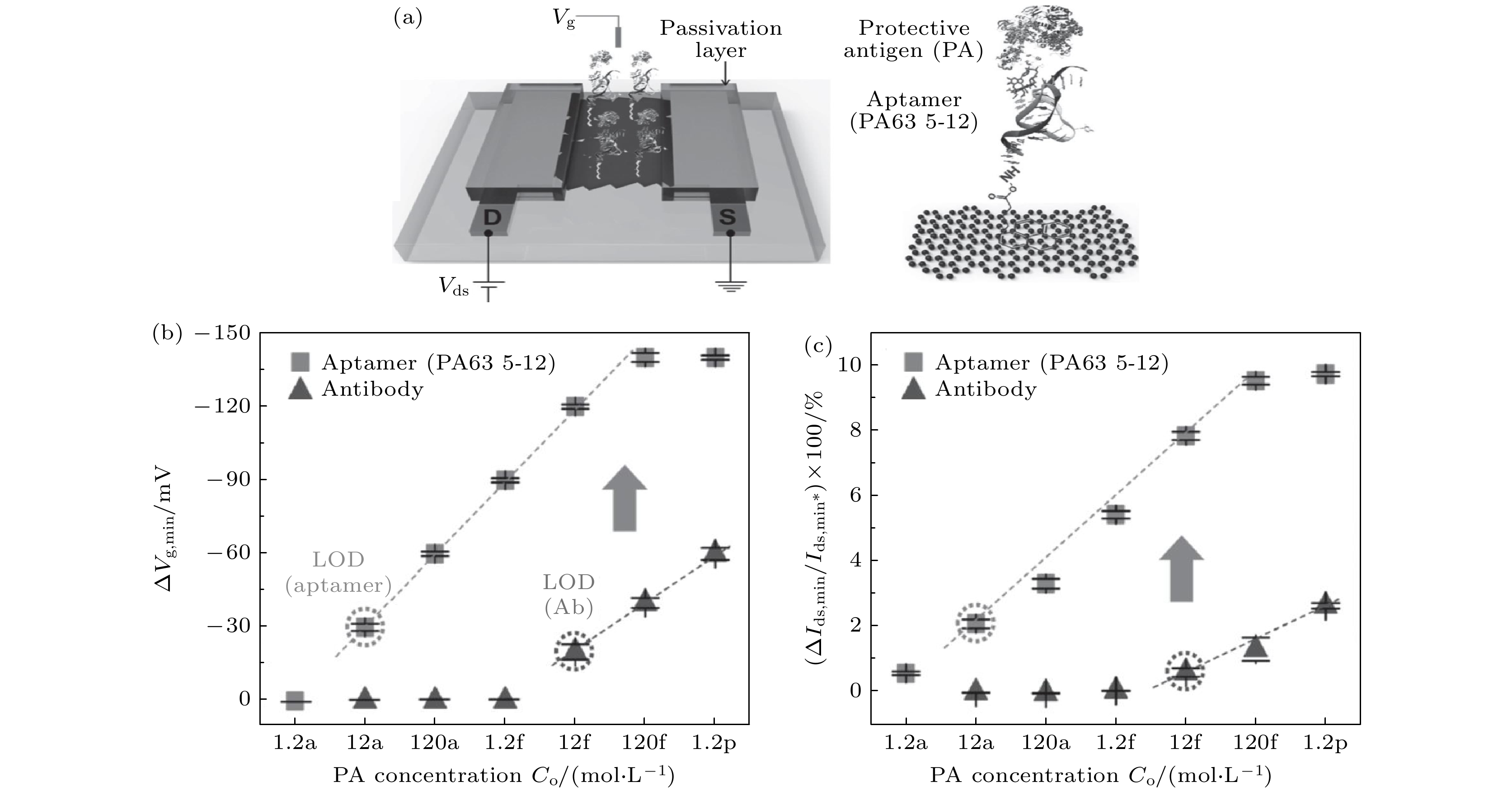 图 6 (a) 适配体修饰在石墨烯场效应晶体管用于抗原检测的示意图; (b) 狄拉克点偏移电压与抗原浓度的关系图; (c) 漏端电流变化值与抗原浓度的关系图, 检测器件为适配体修饰的石墨烯FET和抗体修饰的石墨烯FET[68]
Figure6. (a) Schematic illustration of the aptamer-immobilized graphene FET for detection of protective antigen (PA); (b) Vg,min shift (ΔVg,min) vs. PA concentration in PBS solutions with different probe molecules. The ΔVg,min value was obtained by calculating the difference in charge neutrality point, Vg,min, as a reference for the device with no binding of PA; (c) change in the minimum source-drain current (Ids,min), ΔIds, min/


除了DNA适配体用于生物检测外, DNA单链也可以修饰FET传感器来精准检测某一特定序列DNA链. 如图7所示, 一个石墨烯阵列生物传感器被集成在电路板上, 顶上装配了一个用PDMS制成的微流道通道. 此外他们开发了一项选择性修饰DNA探针的技术, 利用这种技术可以选择修饰的位点. 利用DNA选择性修饰技术, 这个装置可实现对流过微流道的同一液体分别检测不同DNA的浓度[70]. 近年来, 利用DNA折纸技术可以在传感界面处构筑形态各异的分子级结构, 有效改善器件灵敏度和检测极限.
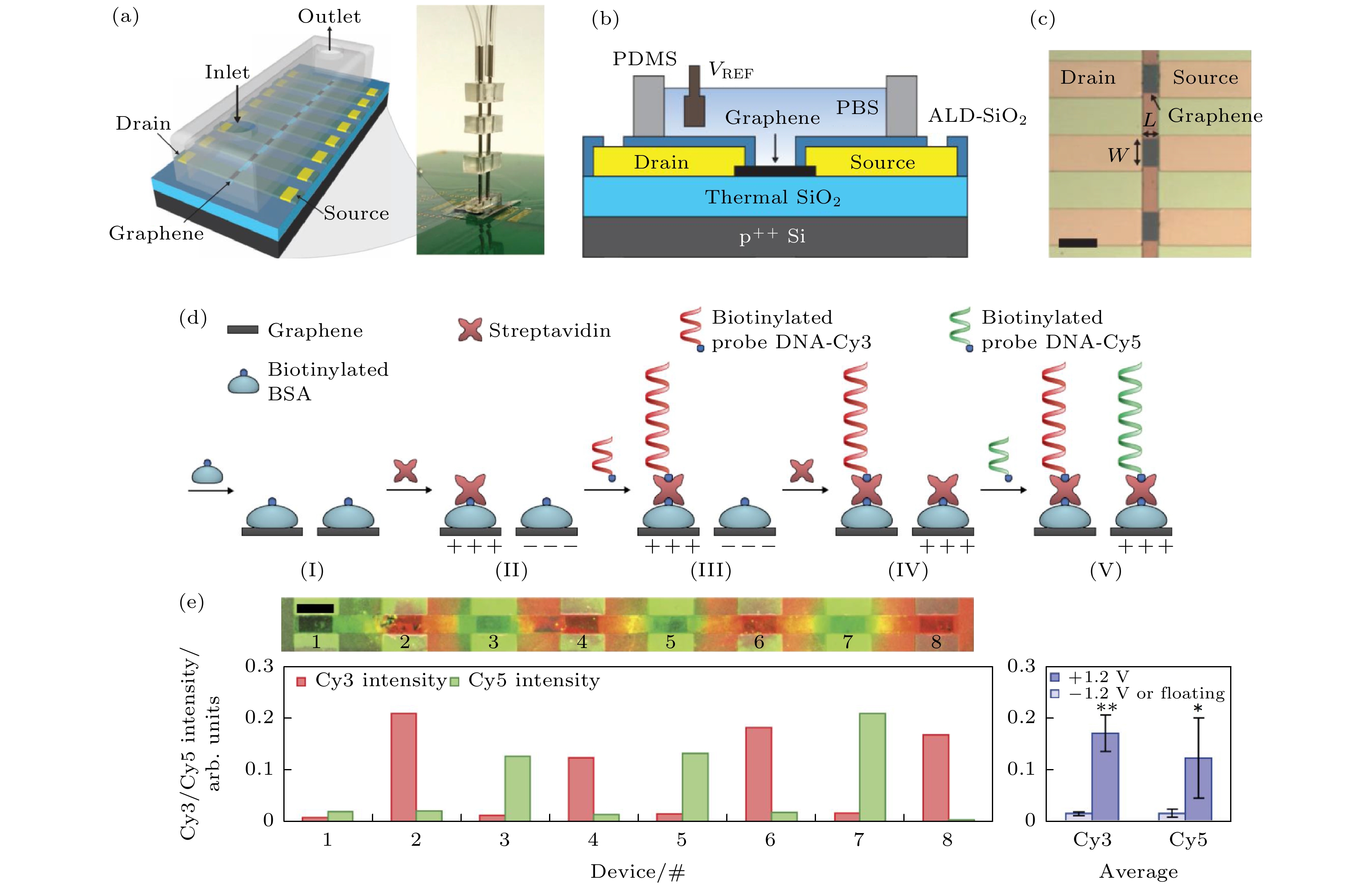 图 7 (a) 石墨烯场效应晶体管阵列带有一个微流道通道的示意图; (b) 器件界面示意图; (c) 器件光学显微镜图; (d) DNA探针修饰示意图, 两种DNA通过酰化牛血清蛋白和链霉亲和素连接到石墨烯表面, 其中一种DNA修饰荧光分子Cy3, 另外一种修饰荧光分子Cy5. 先分别在奇数位点施加+1.2 V电压, 偶数位点施加–1.2 V电压, 将带有Cy3的DNA探针固定到奇数位点; 然后在偶数位点加+1.2 V偏压, 奇数位点不加偏压, 带有Cy5的DNA探针被固定到偶数位点上; (e)带有Cy3和Cy5的FET阵列的共聚焦荧光成像图, 其中Cy3发出红色荧光, Cy5发出绿色荧光[70]
Figure7. (a) Illustration and image of an 8-graphene-electrode/FET array with a microfluidic channel on top. This entire device sits on a printed circuit board. (b) Cross-sectional illustration of an individual graphene site. (c) Optical micrograph of a portion of a fabricated graphene array. For an individual graphene site, W = 90 μm and L = 45 μm (scale bar, 120 μm). (d) During the immobilization of Cy3-labelled probe DNA and associated streptavidin, even- (odd-) numbered sites are biased at 1.2 V (–1.2 V) (20 and 120 s for streptavidin and Cy3-labelled probe DNAs, respectively). During the subsequent immobilization of Cy5-labelled probe DNAs and associated streptavidin, the even- (odd-) numbered sites are left unbiased (biased at 1.2 V), with the same timing scheme as before. (e) Confocal fluorescence image (false coloured) of the array with Cy3 and Cy5 probe DNAs shown, respectively, as red and green, and the corresponding normalized fluorescence intensity. The averaged fluorescence intensities across the four even-numbered and four odd-numbered graphene sites with Cy5 intensity are normalized to the maximum Cy3 intensity; *P < 0.05; **P < 0.01; error bars represent ± 1 s.d. Scale bar, 100 μm[70].
2
2.6.磷脂膜修饰生物传感界面
在生物传感过程中, 通常需要受体分子来识别和捕获目标分子. 如果这些受体分子处于生物友好的环境(磷脂细胞膜)中, 其探测性能可以得到优化. 如图8所示, 活性磷脂分子能以微米级精度在石墨烯衬底表面特定的位置组装出特定尺寸的薄膜. 在磷脂膜上的键对碳具有亲和力, 使其在石墨烯衬底上的流平性非常好, 可以形成单分子层磷脂膜. 并且磷脂薄膜可以连接一些官能团, 这也使得磷脂膜拥有修饰纳米生物探针的能力, 证明了它在生物传感上拥有的巨大潜力. 如图8(d)所示, 链霉亲和素可以特异性地连接在磷脂膜上而不连接在牛血清蛋白上. 通过链霉亲和素的特异性修饰, 可将所需要的抗体连接到链霉亲和素上, 从而制备一个具有特异性识别能力的石墨烯生物传感器[71]. 在传感界面处精准构筑这类生物分子, 可以有效调控传感过程中的背景环境, 为传感过程提供一个更加友好的生物环境.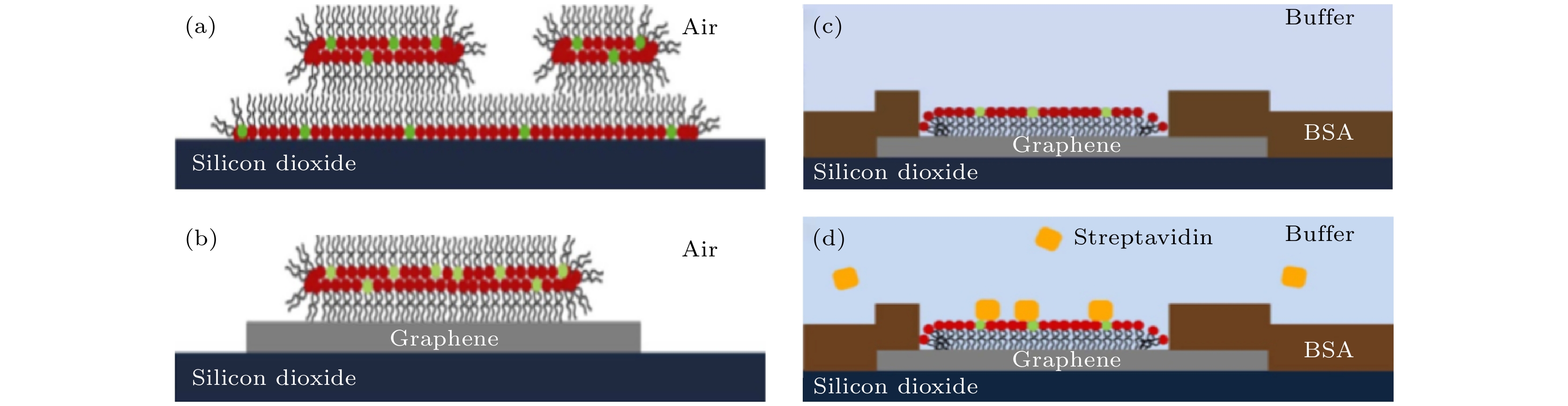 图 8 磷脂膜在二氧化硅和石墨烯上的示意图 (a) 部分区域单层、部分区域双层的磷脂膜在二氧化硅上; (b) 双层磷脂膜修饰在石墨烯表面; (c) 在石墨烯衬底上的单层磷脂分子被牛血清分子包围; (d) 链霉亲和素被特异性绑定在生物酰化的基团上, 牛血清蛋白阻止了链霉亲和素的非特异性绑定[71]
Figure8. Proposed membrane organization on silicon dioxide and graphene. 1, 2-dioleoyl-sn-glycero-3-phosphocholine (DOPC) headgroups are marked in red, Biotin-PE headgroups in green. (a) Base monolayer and additional bilayer on silicon dioxide in air; (b) single bilayer on graphene in air and (c) monolayer of phospholipids on graphene surrounded by bull serum albumin (BSA) layer under water; (d) streptavidin can later be bound to the biotinylated headgroups of the phospholipids from solution with BSA and DOPC preventing unspecific binding to the substrate[71].
2
2.7.有机小分子修饰生物传感界面
生物传感器通常大多数靠抗体、DNA、核酸适配体等受体分子来捕获目标物, 从而对FET的沟道表面进行电学掺杂. 但面对一些寿命很短的检测物时, 利用受体分子检测目标分子的方法就会失效. 当检测物寿命很短时, 利用剪切反应则能快速检测目标分子. 图9所示为一个超高灵敏度的羟基自由基的石墨烯FET传感器. 羟基自由基超高的反应活性和超短的寿命阻碍对其进行高灵敏度的检测. 这个器件则是利用羟基自由基的内剪切反应来改变原卟啉对石墨烯沟道的电学掺杂, 从而实现超低检测极限(10–9 mol/L)的实时检测(2 s). 这种在传感界面处精确构筑一些化学小分子, 从而精准控制被检测分子的相关化学反应, 为超短寿命物质的检测提供了有效而可靠的方法[72]. 图 9 (a) 石墨烯FET传感器传感机制示意图; (b) 液栅晶体管I-V曲线, 四条曲线分别为纯石墨烯晶体管转移曲线(黑色), 经历金纳米颗粒/半胱胺-原卟啉修饰石墨烯FET的转移曲线(红色), 经历金属离子修饰后石墨烯FET的转移曲线(10–4 mol/L Cd+, 绿色), 经历剪切反应后石墨烯FET的转移曲线(10–4 mol/L·OH, 蓝色); (c), (d) 石墨烯/金/半胱胺-原卟啉传感器对铬离子和羟基的实时响应曲线 (1 M = 1 mol/L)[72]
Figure9. Detection performance and mechanism of the FET sensor: (a) Schematic diagram of the ·OH detection; (b) liquid gate transfer curves of a FET device of pristine graphene (black), after decoration of gold nanoparticle/cysteamine-protoporphyrin (red), after metallic ions (10–4 mol/L Cd2+, green), and after shear reaction (10–4 mol/L ·OH, blue), when liquid gate voltage (Vg) varies from –400 to 800 mV; (c), (d) real-time electrical responses of a graphene/Au/Cys-PP FET device upon successive addition of Cd2+ and subsequent ·OH[72].
2
2.8.二维材料的三维结构界面构筑
生物传感过程中, 除了对表面进行修饰不同的生物探针来构筑传感界面之外, 还可以对二维材料的几何结构进行改造, 构建一些基于二维材料的三维结构来提升传感界面的性能. 如图10所示, Hwang等[73]利用预拉伸衬底, 然后在110 ℃下退火, 石墨烯随着柔性衬底一起褶皱, 产生纳米结构的褶皱石墨烯薄膜. 这类具有纳米结构的石墨烯薄膜有效增加了传感界面的德拜长度, 在褶皱结构的凹陷处, 其德拜长度远大于平坦石墨烯的德拜长度. 因此, 凹陷处DNA链将有更多的碱基对能够对石墨烯产生电学掺杂效应, 极大提升了传感信号, 降低了生物传感器的检测极限(检测极限为600 zmol/L在缓冲溶液中, 20 amol/L在人血清溶液中).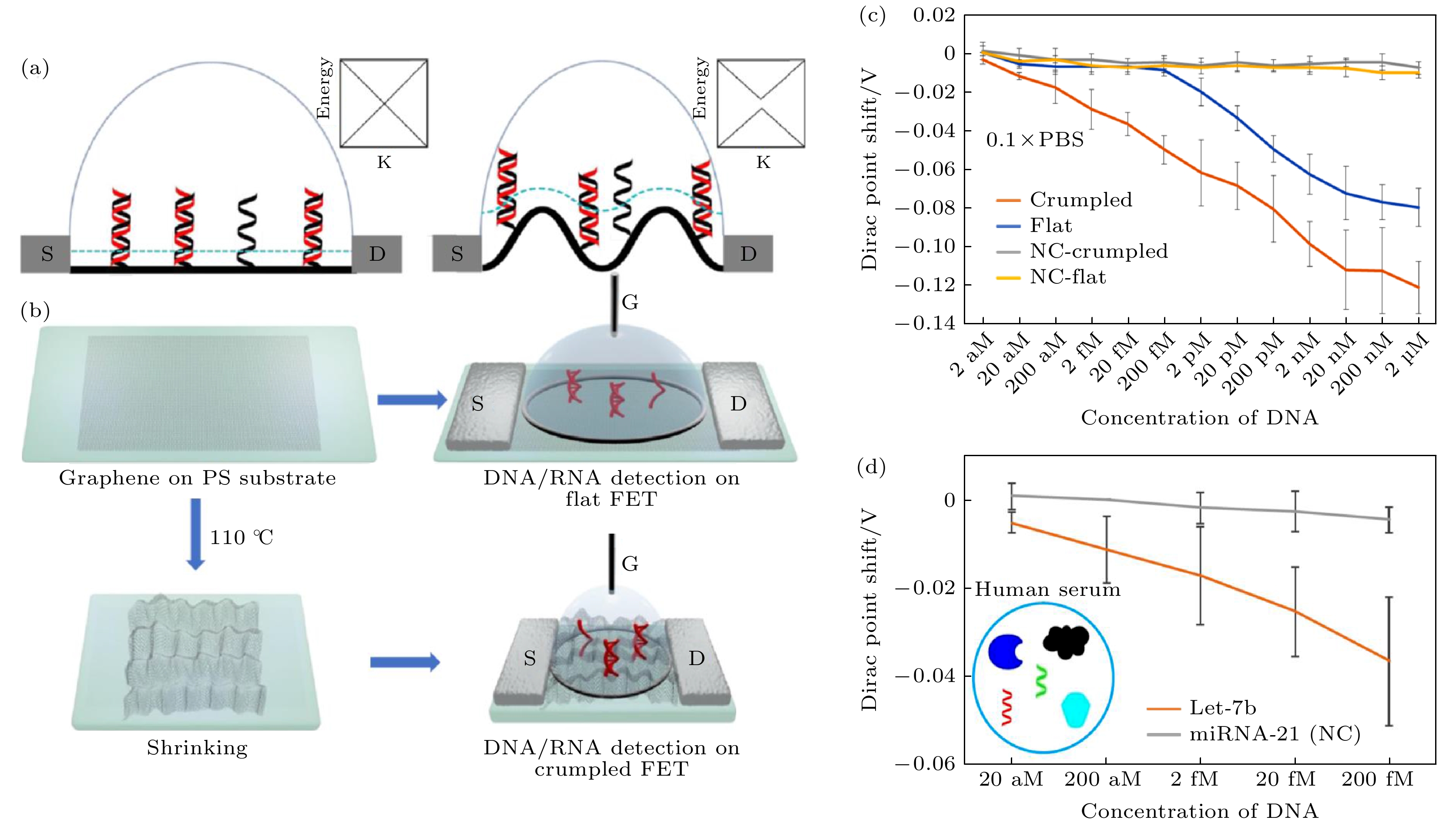 图 10 (a)平坦石墨烯晶体管DNA传感器和褶皱石墨烯晶体管DNA传感器的截面示意图, 黑色为探针DNA, 红色为目标DNA链, 蓝色线代表德拜长度, 在凹陷结构中的DNA链有更长的部分在德拜长度以内; (b)平坦石墨烯晶体管和褶皱石墨烯晶体管的制作流程示意图; (c)狄拉克点偏移量与被测DNA浓度关系图 (1 M = 1 mol/L); (d)在人血清中, 石墨烯狄拉克点偏移与被测DNA浓度关系图[73]
Figure10. (a) Cross-sectional scheme of the flat (left) and crumpled (right) graphene FET DNA sensor. Probe (black) and target (red) DNA strands are immobilized on the surface of graphene. The blue dot lines represent Debye length in the ionic solution and the length is increased at the convex region of the crumpled graphene, thus more area DNA is inside the Debye length, which makes the crumpled graphene more electrically susceptible to the negative charge of DNA. (b) Fabrication of FETs and experimental process flow. Graphene on pre-strained PS substrate was annealed at 110 °C to shrink the substrate and crumple the graphene. Then source and drain electrodes were applied and solution-top gate was used. In case of flat graphene FET, the annealing process was omitted. (c) Dirac voltage shift of the FET sensor with detection of hybridization using DNA probe. NC is non-complementary control sequences used in the experiments. (d) Dirac voltage shift of the FET sensor with miRNA detection of hybridization. Target RNA spiked in human serum was treated on the FET sensor. Human serum is complex mixture of biological components[73].
2
3.1.等离激元共振传感界面构筑
光学生物传感器的界面修饰工程和电学生物传感器是相似的, 都是通过表面的DNA链或者适配体来捕获目标分子(DNA、生物分子、金属离子等). 但是, 基于光学原理的生物传感器在捕获目标分子后产生的通常是光学信号的变化, 比如表面等离激元共振吸收峰的偏移、荧光猝灭等. 如图11所示, Zeng等[76]构筑了一个石墨烯-金的超表面结构, 在表面等离激元导致电场最强时, 产生了一个相位奇变点, 这一奇变点对石墨烯-金周围介质极度灵敏, 当有物质吸附到石墨烯表面, 奇变点处的相位就会产生很大的变化. 此外, 利用石墨烯的SP2轨道杂化结构, 可与带有苯环的生物分子形成π-π相互作用, 有效地捕获一些生物分子, 如DNA、细胞因子等. Kravets等[77]利用石墨烯与金纳米锥阵列形成的强耦合, 在600 nm处产生一个强相位奇点, 实现单分子检测. 除了利用生物探针捕获检测物之外, 分子的振动指纹也可以用于检测化学分子. Daniel等[78]利用石墨烯纳米带阵列在中红外产生的强等离激元, 放大了分子振动的吸收峰, 实现了对化学分子的精准识别.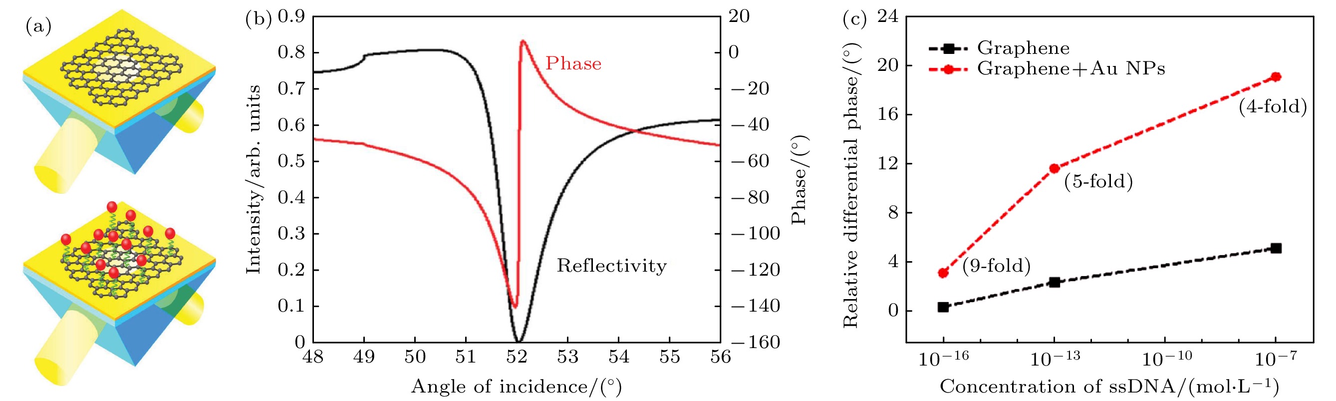 图 11 (a) 石墨烯超表面设计, 将石墨烯沉积在金表面; 为了激发石墨烯-金界面处表面等离激元极化, 一束光通过一个玻璃棱镜照射在50 nm金薄膜上, 然后反射到另外一个面; 金纳米颗粒连接到DNA上作为SPR增强的标签; (b) 光的反射率(黑线)和相位(红线)作为光照射在石墨烯-金界面处入射角的函数, 其中, 相位在SPR曲线最小值处经历了一个奇变点; (c) 对比了纯石墨烯和石墨烯加金纳米颗粒(石墨烯先利用π-π相互作用与DNA连接, 然后将金纳米颗粒连接到DNA上, 从而增强DNA检测信号)两种器件对单链DNA浓度检测的信号强度[76]
Figure11. Designs of graphene-gold metasurface architectures. (a) Basic architecture with a layer of graphene deposited on the gold surface. To excite surface plasmon polariton over the graphene-gold interface, a light beam is typically passed through a glass prism and reflected from a 50 nm gold film deposited on one of its facets. (b) Calculated reflectivity (black) and phase (red) of light as functions of the angle of light incidence of the gold-graphene interface, corresponding to maximum probing field. Phase experiences a sharp singularity in the minimum of SPR curve. (c) Response and magnitude of enhancement (in the bracket) obtained with (circles) and without (squares) exposing the monolayer graphene-coated sensing film to positive-charged Au NPs after ssDNA[76].
2
3.2.荧光共振能量转移生物传感界面构筑
由于石墨烯具有很强的荧光猝灭能力(远超过传统有机材料)和生物相容性, 基于荧光共振能量转移的石墨烯生物传感器也引起了大量的研究. 他们被广泛应用在DNA、蛋白质和金属离子的检测中. 金属离子检测主要基于其与寡核苷酸相互作用这一原理. 例如, 基于银离子与胞嘧啶、汞离子与胸腺嘧啶特殊的相互作用, 一系列银离子与汞离子传感器被制造. 如图12(a)所示, Wen等[79]利用含有胞嘧啶的寡核苷酸与氧化石墨烯(GO)耦合形成的生物传感器检测银离子. 当银离子被添加进溶液中, 带有荧光标记的寡核苷酸探针形成茎环结构, 增加了氧化石墨烯与荧光分子的距离, 使其不再被氧化石墨烯猝灭. 荧光强度提供了银离子量化的可读数据, 这个传感器展示了优异的特异性识别能力和较低的检测极限(5 nmol/L), 这一浓度达到了美国环境保护机构饮用水的标准. 其他科研人员也利用这一传感机制并进一步调节器件设计, Cui等[80]利用石墨烯量子点作为荧光标记替代传统的荧光染料, 发展了一个超灵敏的汞离子传感器.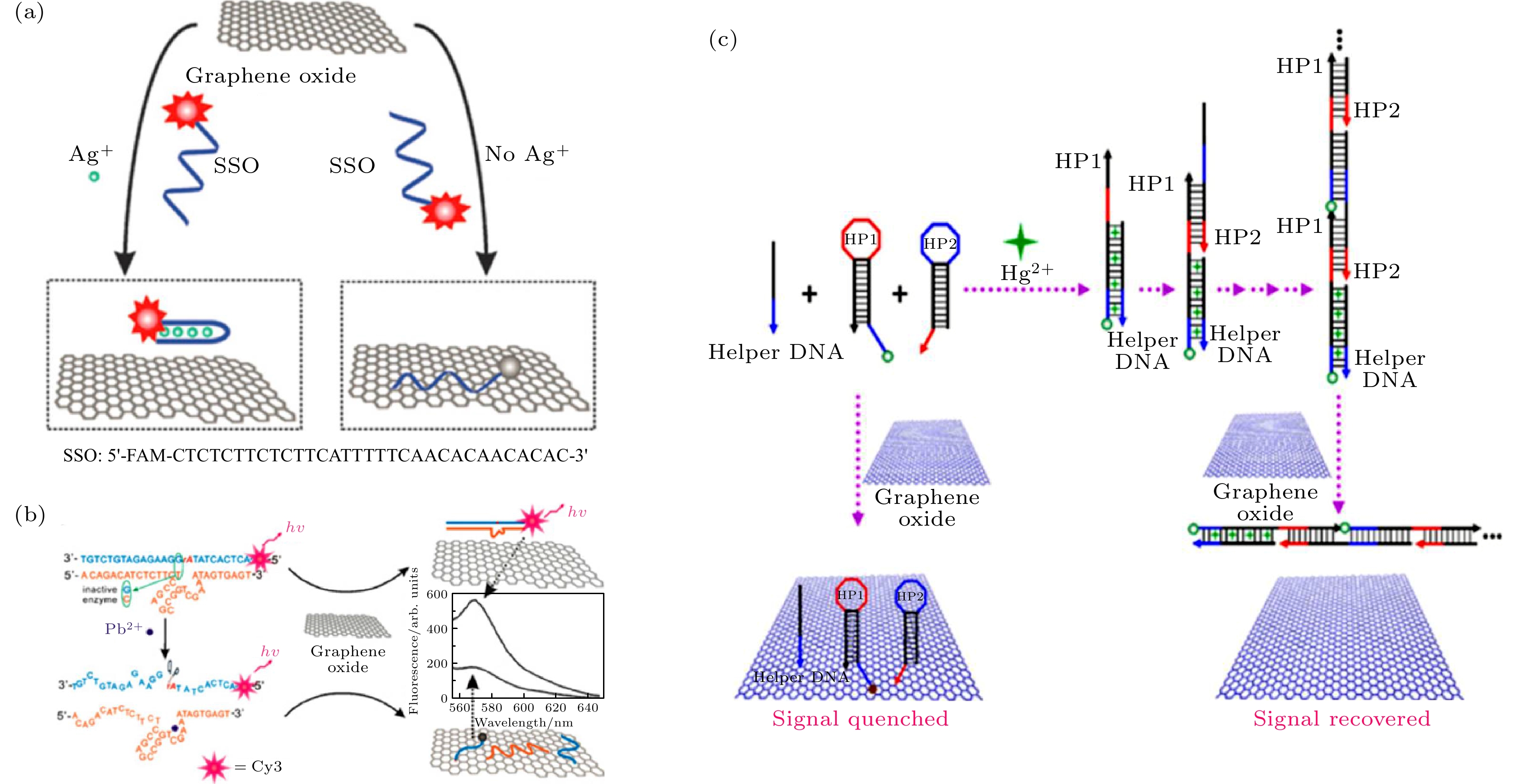 图 12 (a) 银离子荧光传感器示意图, 特异性识别银离子的DNA链在和银离子相互作用后导致DNA链构型改变, 从而DNA链从氧化石墨烯上脱附, DNA所携带的荧光分子产生荧光[79]; (b) 铅离子调节DNA酶与氧化石墨烯的相互作用的示意图[81]; (c) 汞离子探测机制示意图[82]
Figure12. (a) Schematic illustration of the fluorescence sensor for Ag+ ions based on the target-induced conformational change of a SSO and the interactions between the fluorogenic silver-specific oligonucleotide probe and graphene oxide (GO)[79]. (b) Schematic for the Pb2+-modulated interactions between DNAzyme and GO. Inset is the fluorescence spectrum of a mixture of DNAzyme and GO upon interaction with 0 mol/L (top curve) and 2 mmol/L (bottom curve) of Pb2+ in a Tris-HCl buffer (50 mmol/L, pH = 7.4) solution containing 50 mmol/L NaCl[81]. (c) Schematic of the proposed detection mechanism (for clarity, pristine graphene is used to represent GO)[82].
酶和氧化石墨烯的耦合功能化也构建了一些新型荧光生物传感器. 如图12(b)所示, Fan等[81]研究了铅离子与8-17 DNA酶的相互作用, 他们基于铅离子可剪切17S链原理, 从而调节8-17 DNA酶与氧化石墨烯相互作用, 制备了一个灵敏的铅离子传感器. 被剪切后的DNA酶变成DNA单链被吸附在氧化石墨烯表面, 荧光标记被氧化石墨烯猝灭, 从而通过猝灭的荧光信号强度来量化铅离子浓度[81]. 除此之外, 为了进一步改善传感器灵敏度, 许多信号扩增方法被尝试. 一个典型的信号扩增方案是利用杂化链式反应来实现荧光信号扩增, 如图12(c)所示. 两个发夹探针和一个辅助DNA被设计和应用, 当汞离子被加入溶液中, 杂化链式反应通过汞离子和辅助DNA开启. 杂化链式反应产生的双链DNA从氧化石墨烯表面脱附, 荧光信号被检测到. 这类基于杂化链式反应的传感器展现了高的灵敏度和选择性, 检测极限为0.3 nmol/L, 展示了其在生物检测中极大的潜力[82].
1)当前二维材料价格昂贵, 高质量单晶二维材料的大面积生长仍然存在问题. 探索低成本、高质量、大面积的高效合成方法是推动二维材料实际应用的重要课题.
2)二维材料传感功能界面构筑通常利用化学方法实现, 缺点是难以精准控制传感功能界面的生物探针位置与密度, 从而导致各批次器件的均一性还不够理想. 因此, 对于传感功能界面生物探针位置及密度的精确控制至关重要.
3)与实际需求结合, 发展二维生物传感器的商业化示范应用, 为最终大规模应用打开突破口.
