全文HTML
--> --> -->当石墨烯沿某一平面方向的宽度减小到几十纳米到几纳米时, 由于量子限域效应和边界效应, 这些石墨烯纳米带(graphene nanoribbons, GNRs)将出现电子能量禁带[7]. 石墨烯纳米带模型的提出可上溯到1996年由Fujita等[8]通过紧束缚方法计算得出的具有不同边界的纳米带. 随后的理论计算表明[9-12], 不同边缘构型的纳米带具有不同的电子结构及性质. 其中锯齿型石墨烯纳米带(zigzag graphene nanoribbons, ZGNRs)在费米面附近存在局域化边界态, 表现为金属性; 而扶手椅型石墨烯纳米带(armchair graphene nanoribbons, AGNRs)的性质随宽度变化发生周期性改变. 自2010年Cai等[13]首次用有机分子自组装方法合成原子级的纳米带以来, 各种宽度的纳米带相继被制备出来[14-21], 能带结构也得到了研究. 有机分子自组装方法是用热蒸发的方式将设计好的含有卤族元素的前驱体分子蒸发到保持在低温的单晶金属基底上, 如Au单晶等, 在金属基底的催化作用下, 前驱体脱去卤族元素, 形成自由基, 分子通过自由基之间C—C键聚合形成分子链. 然后将样品加热到更高的温度, 分子链内部发生环化脱氢反应形成GNR. 由于GNR的结构完全取决于前驱体分子构型, 因此这种方法得到结构精确可控的GNR, 从而可以调控GNR的电学特性. Zhang等[14]选取(1, 4, 5, 8-四溴萘)作为前驱体分子, 分别在370和470 K经过脱卤和脱氢环化反应制备出N = 5(N表示沿纳米带宽度方向上的碳原子层数)的AGNR, 并测出其带隙为2.8 eV. 这一结果与之后Kimouche等[15]通过实验得到的长度为5 nm的N = 5的AGNR的带隙有较大差异, 差异可能来自于纳米带长度或其他因素的影响. Talirz等[18]将前驱体分子(二溴-邻三联苯)加热蒸发沉积到金属基底Au(111)上, 在150 ℃发生了脱溴反应, 在250 ℃, 分子在表面扩散, 并在自由基位置结合, 形成分子链, 进一步加热到350 ℃时, 分子链内发生了脱氢环化形成N = 9的AGNR, 并测出其带隙为1.4 eV. 实验时基底和探针的极化作用会对测得的带隙值有影响.
当把分子放置于强外电场时, 这些分子将会产生一些新的物理化学现象, 如化学键碎裂、新激发态产生、新自由基出现以及斯塔克效应等[22-29], 从而对分子的结构、能隙及光谱等产生影响. 在对石墨烯纳米带的电子结构进行调控方面, 可以通过引入外加电场的方法来破环纳米带的结构对称性, 进而影响其电子结构. Son等[30]采用在平面内施加沿锯齿型纳米带宽度方向的横向电场, 使纳米带两边界的静电势不同, 破坏两端自旋态的能量简并, 导致一种自旋态出现在费米能级处, 而另一种自旋态不在费米能级处, 使纳米带呈半金属性. Chang等[31,32]通过紧束缚方法计算发现, 外加电场对扶手椅型纳米带的色散关系、能隙及态密度等有显著的影响, 并且还会引起半导体-金属转变. 但外加电场对纳米带内电子分布的影响以及电场强度值对纳米带带隙变化的影响, 特别是对未加氢钝化的纳米带现尚不多见于相关研究.
本文采用基于密度泛函理论的紧束缚方法(density functional tight binding, DFTB), 对不同均匀电场强度下, 不同边缘构型的扶手椅型石墨烯纳米带进行计算, 探究电场对纳米带电子结构的影响并对其电子布居数的变化进行分析. 这里的计算对象选取为扶手椅型石墨烯纳米带, 是因为这种纳米带表现出明显的半导体性质, 并且它的性质明显受到纳米带宽度的影响. 在通过物理方法或化学方法制备的纳米带边缘往往都具有悬挂键, 这会使得结构不稳定, 为了稳定结构, 通常对其边缘进行一定的处理, 其中最常用的便是对纳米带边缘加氢原子, 所以本文对纳米带分别考虑不施加边缘钝化和施加边缘钝化两个情况. 相较于第一原理和经典分子动力学计算, 基于量子力学原理的紧束缚方法所计算体系内的原子数远多于第一原理计算, 同时还可以给出分子动力学计算所很难给出的电子结构信息, 现在针对典型半导体材料, 已有较多DFTB的计算研究[33-37].


在施加外电场后, 能量表达式变为[42]


纳米带的初始结构模型如图1所示, 计算时考虑不加氢(图1(a))和加氢(图1(b))两种情况. 图中, N表示沿纳米带宽度方向上碳原子层数, E为所施加横向电场方向, 方框内为沿纳米带长度方向上一个最小的结构单元. 图1(b)中纳米带边缘的黑色圆圈表示所加的氢原子. 将纳米带的宽度设为W, 则W与N的关系如下:
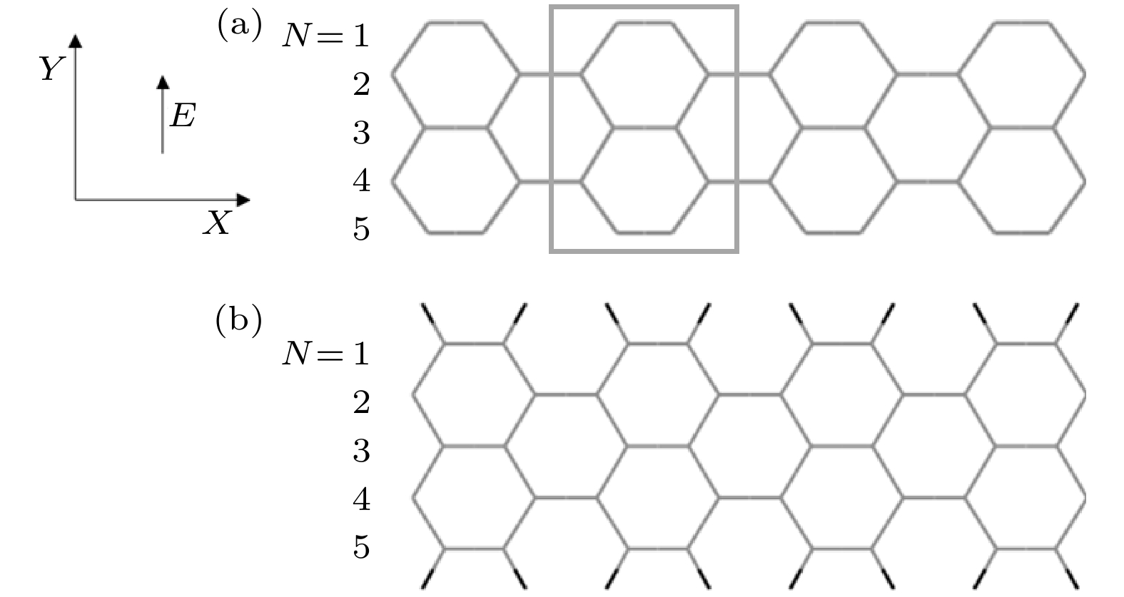 图 1 (a) N = 5的未加氢钝化的纳米带; (b) N = 5的氢钝化的纳米带
Figure1. (a) Un-hydrogenated nanoribbons with N = 5; (b) hydrogenated nanoribbons with N = 5.
首先进行SCC结构优化, 设定两个经SCC过程后的电荷差阈值为1.0–5, 当小于该阈值时停止计算, 随后对经结构优化后的各纳米带在施加电场后再进行自洽电荷计算.
在计算能带结构和态密度时, 沿布里渊区的高对称线指定了K点分别为Γ(0,0,0)和X(0.5,0,0), 并在这两个点之间的连线选择了26个采样点.
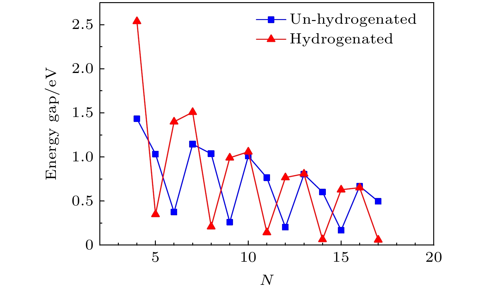 图 2 不同宽度的氢化/未氢化的扶手椅型石墨烯纳米带在Г点处的能隙
Figure2. Energy gap of hydrogenated/un-hydrogenated armchair graphene nanoribbons with different widths.
图3给出了N = 5的未加氢纳米带带隙随电场强度的变化. 如图中所示, 带隙整体上呈现出随电场强度的增加先减小后不变的趋势, 在电场强度为0—2 eV时, 带隙随电场强度增加而减小得较慢; 随后带隙减小较快, 直到电场强度为5 V/nm时; 当电场强度大于5 V/nm时带隙几乎为0. 这里采用DFTB方法计算得到的N = 5纳米带的带隙为1.1 eV, 这个值小于实验值, 但可确定纳米带具有半导体性, 这与实验测量结果一致. 这种差异是因为作为半经验的DFTB计算并不是薛定谔方程的精确解, 计算结果与实验值会存在一定差异, 但在定性预测材料性质上, DFTB计算仍可以提供足够的准确度, 如存在电场强度的阈值, 即当所施加电场强度高于此阈值时, 带隙为零[43].
 图 3 N = 5的未加氢钝化的纳米带的带隙随电场强度的变化
Figure3. Band gap of un-hydrogenated nanoribbons with N = 5 under different electric field intensity.
图4和图5给出了N = 5的未加氢纳米带及边缘加氢钝化的纳米带在电场强度分别为0, 3, 5 V/nm时, 费米能级(EF)附近的的能带结构及态密度(–4—4 eV的能量区间). 电场强度为0对应没有施加电场的情况. 在这两个图的能带图中, 可以区分出导带和价带两部分, 这样导带最低点与价带最高点能量之差即为其带隙. 在纳米带中, 碳的2s轨道与2px和2py轨道相互作用, 形成三个sp2杂化轨道, 三个sp2轨道相互作用形成三个σ键, 这是一种很强的共价键, σ键将电子定域在连接两个碳原子的平面内. 由2pz电子形成的π键, 其成键电子云与碳原子平面垂直, 这种π电子与原子核间的相互作用较弱, 易受外界因素的影响. 在能带计算中, σ电子相对于π电子, 分布在低能量区域, 费米能级附近的电子态由π电子贡献.
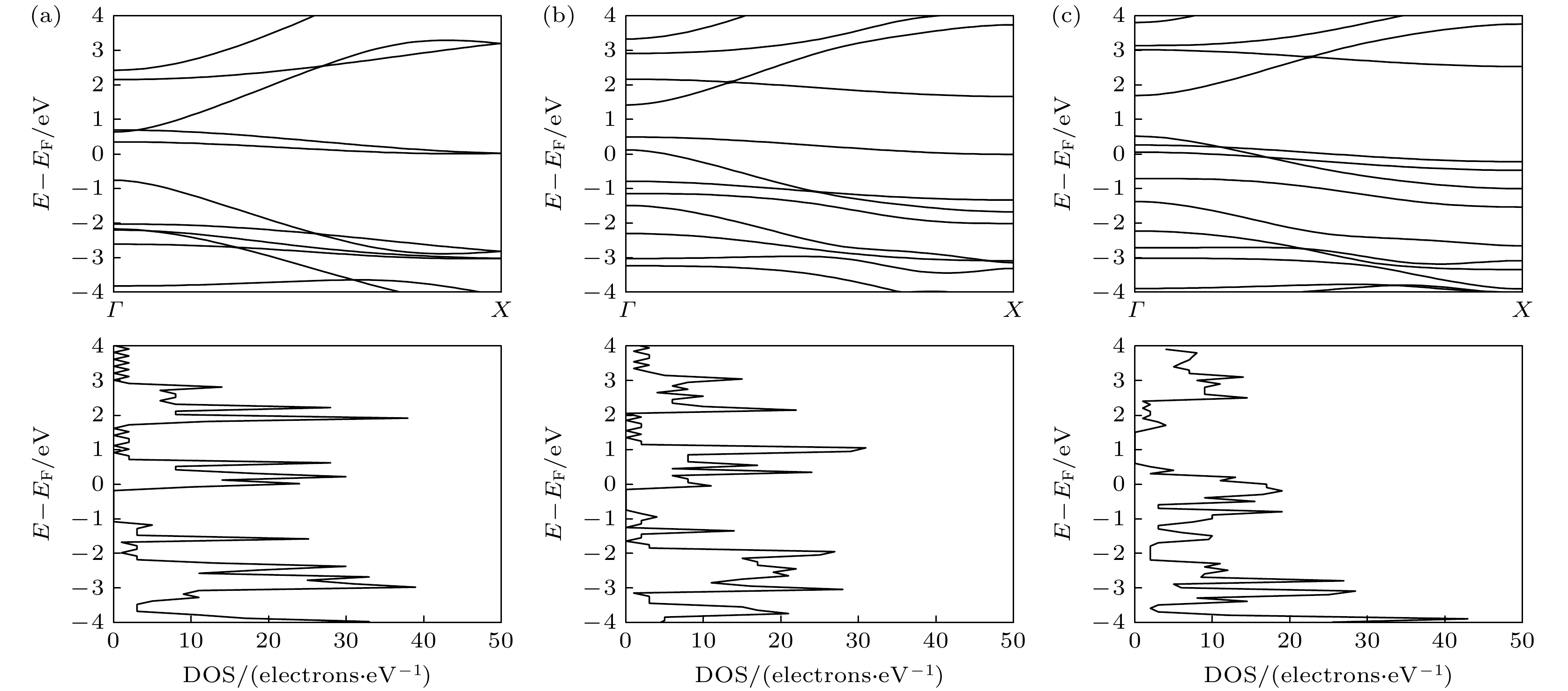 图 4 不同电场强度时N = 5的未加氢钝化的纳米带的能带结构及态密度 (a) E = 0 V/nm; (b) E = 3 V/nm; (c) E = 5 V/nm
Figure4. Band structure and density of states of un-hydrogenated nanoribbons with N = 5 under the external electric field: (a) E = 0 V/nm; (b) E = 3 V/nm; (c) E = 5 V/nm
 图 5 不同电场强度时N = 5的氢钝化的纳米带的能带结构及态密度 (a) E = 0 V/nm; (b) E = 3 V/nm; (c) E = 5 V/nm
Figure5. Band structure and density of states of hydrogenated nanoribbons with N = 5 under the external electric field: (a) E = 0 V/nm; (b) E = 3 V/nm; (c) E = 5 V/nm.
如图4所示, 不加电场时N = 5的纯纳米带能带结构表现出间接带隙半导体的特点, 带隙为1.08 eV, 在加电场后其能带结构与不加电场时相比, π电子受到电场的影响, 其所在能级发生明显改变, 使得费米能级附近能带线的位置发生移动. 由图4(b)可见, 当电场强度为3 V/nm时, 价带顶部能带线上移, 使得带隙值有所减小, 带隙值减少到0.6 eV. 随着电场强度增加到5 V/nm时, 原价带部分的能带线穿过费米能级, 能带结构表现为金属性, 纳米带发生半导体-金属转变. 由态密度图同样可以看出, 在不加电场及电场强度为3 V/nm时, 纳米带在费米能级附近的态密度为零, 表现出半导体性. 但当电场强度为5 V/nm时, 费米能级附近同样被电子能级填充, 能隙消失, 表现出金属性. 并且态密度峰的位置及大小同样会随电场强度的不同发生变化.
对于N = 5的边缘氢钝化的纳米带, 当不加电场时, 由于氢原子的存在, 边缘处碳原子和氢原子形成C—H键, 纳米带的边缘态发生改变, 从而影响纳米带的电子结构, 使得价带部分能带线上移穿过费米能级, 纳米带表现出金属性. 在加电场后, 随着电场强度的增加, 能带线有所变化, 但始终表现出金属性. 相应地在态密度图中, 费米能级始终被电子能级所填充.
对晶体中Mulliken电子布居数的分析有助于了解晶体结构的稳定性, 同时通过对各晶体内各原子上电子布居数的变化, 可以定性反映原子间的电荷转移情况. 图6和图7分别显示了包含5个原子层的未加氢纳米带及边缘氢钝化的纳米带一个结构单元内各原子上的电子布居数, 图中用不同颜色的小球表示各原子所具有的布居数. 计算中由于仅考虑C原子的2s和2p价电子, 故中性C原子的电子布居数为4.0. 如图6(a)所示, 未施加电场时, 布居数呈现出完全对称的分布, 其中第二层原子和第四层原子的布居数最小, 为3.92, 处于失去电子的状态, 从该两层原子向中心和两边, 布居数逐渐增大, 中心原子的布居数约为4.01, 边界处布居数最大, 约为4.07. 施加电场后, 由于沿Y轴正方向电场的存在, 各层原子上的布居数分布不再对称, 第三层碳原子的布居数基本不发生变化, 约为4, 处于稳定状态; 同时第一二层的电子向第四五层迁移. 随着电场强度的增大, 布居数分布不对称的现象越发明显, 最大和最小布居数之差也随之增大.
 图 6 不同电场强度下N = 5的未加氢钝化的纳米带的电子布居数 (a) E = 0 V/nm; (b) E = 3 V/nm; (c) E = 5 V/nm
Figure6. The electron population of un-hydrogenated nanoribbon with N = 5 under the external electric field: (a) E = 0 V/nm; (b) E = 3 V/nm; (c) E = 5 V/nm.
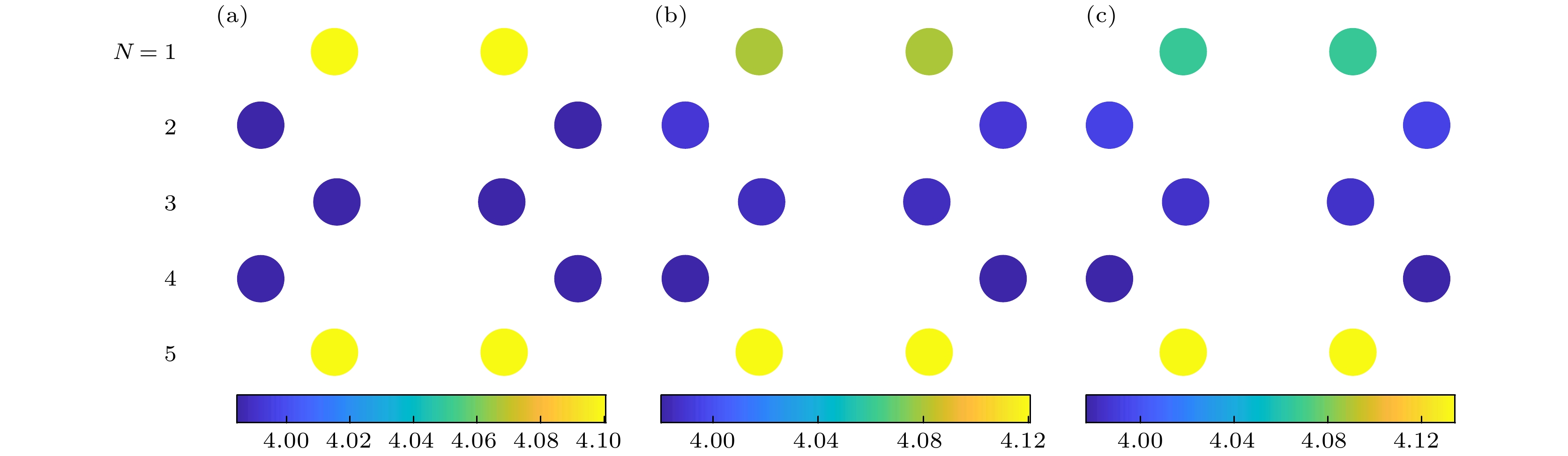 图 7 不同电场强度下N = 5的氢钝化的纳米带的电子布居数 (a) E = 0 V/nm; (b) E = 3 V/nm; (c) E = 5 V/nm
Figure7. The electron population of hydrogenated nanoribbon with N = 5 under the external electric field: (a) E = 0 V/nm; (b) E = 3 V/nm; (c) E = 5 V/nm.
对于纳米带加氢钝化后的情况, 由图7可见, 各层内原子电子布居数的分布较未加氢情况明显变得均匀, 电子的得失主要发生在位于纳米带边缘区域的原子, 这时由于边缘所加的氢原子会向碳原子提供电子, 这样会导致纳米带中碳原子的布居数大于未加氢纳米带中碳原子上的布居数. 如图7(a)所示, 无电场时, 纳米带各原子层内电子的布居数表现出完全对称的现象. 这时, 处于最外边缘的原子层内各原子的电子布居数为4.1, 处于中间层内原子的布居数约为4.0, 中间层与外边缘层间两层原子的布居数为3.98, 处于中间的三层原子的布居数很接近. 施加外电场后, 第三层碳原子的布居数基本不发生变化, 电子的得失则发生在边缘区域, 第一层原子的外层电子在电场作用下, 有部分迁移到第二层原子上, 使得第一层原子布居数减小而第二层原子布居数增大; 同样地, 第四层原子布居数减小, 第五层原子布居数增大, 使得第一层原子的布居数小于第五层原子的布居数, 第二层原子的布居数大于第四层原子的布居数. 纳米带内各原子层内原子上的布居数分布不再对称, 并且随着电场强度的增大, 不对称现象也变得越发明显.
对于未加氢钝化的纳米带, 边缘处的碳原子仅与两个相邻碳原子成键而具有悬挂键, 这使得边缘处的碳原子有得到电子以达到稳定结构的趋势, 这时电子从位于次边缘处的碳原子向边缘处和纳米带中心处的碳原子迁移. 在无电场时, 纳米带各原子上的布居数呈现出边缘高-次边缘低-中间稍高的分布情况. 施加电场后, 电子在电场作用下发生定向移动, 纳米带沿电场方向发生极化, 各原子带电量改变, 键长在电场及周围原子的共同作用下发生改变. 随电场强度的增加, 键长变化幅度增大, 第二层原子和第一、三层原子连接的碳-碳键长缩短; 第四层原子和第三五层原子连接的碳-碳键键长拉伸, 在电场强度达到6 V/nm时, 键长变化幅度在0.01 ?. 对于边缘氢钝化的纳米带, 边缘氢原子的存在, 使纳米带的边缘变得稳定, 并显著改变布居数的分布, 键长同样有所变化, 在电场强度达到6 V/nm时, 变化幅度为0.001 ?, 远低于未加氢钝化的纳米带.
由图8可以看出, 未加氢纳米带和边缘加氢钝化的纳米带的最大最小布居数之差随电场强度的增大而均匀增大, 但未加氢纳米带的布居数之差及其增大幅度均大于边缘加氢钝化的纳米带, 说明边缘氢钝化可显著改变纳米带内原子上的布居数分布.
 图 8 N = 5的未加氢钝化/加氢钝化的纳米带最大最小布居数之差随电场强度的变化
Figure8. The difference between the maximum and minimum populations of the un-hydrogenated/hydrogenated nanoribbons with N = 5 varies with the electric field intensity.
