1.Institute of Solid State Physics, Hefei Institutes of Physical Science, Chinese Academy of Sciences, Hefei 230031, China 2.University of Science and Technology of China, Hefei 230026, China 3.School of Mathematics and Physics, Anhui Jianzhu University, Hefei 230022, China
Fund Project:Project supported by the National Natural Science Foundation of China (Grant Nos. 51472247, 51671182) and the Joint Funds of the National Natural Science Foundation of China (Grant No. U1632123)
Received Date:18 September 2020
Accepted Date:22 October 2020
Available Online:05 March 2021
Published Online:20 March 2021
Abstract:With the rapidly increasing demands pertaining to high voltage applications in modern power electronic systems, power devices have become widely used in today’s power applications. As a major carrier device without unreliable metal-semiconductor Schottky contact, super barrier rectifier (SBR) has been one of promising substitutions for traditional diodes since it was first introduced, owing to its excellent performance and reliability. The main principle behind SBR approach is to create an adjustable potential barrier in the MOS channel. The height of this barrier can be easily adjusted by the doping concentration in the channel and by the oxide thickness. Trench-gate-type SBR (TSBR) with a trench gate is so designed that the junction-type field-effect transistor effect of planar gate structure enables TSBR to be eliminated to have ultralow forward voltages and a good tradeoff between the forward voltages and reverse leakage currents. However, the charge coupling effect under reverse bias, which is usually neglected and not intensively studied, plays an important role in determining the breakdown voltage of TSBR for high voltage applications (above 200 V). In this paper, the two-dimensional electric field distribution influenced by the charge coupling effect is explained and verified by the analytical model and device simulations with TCAD software Sentaurus. Adjusting the key parameters including the trench depth, oxide thickness and mesa width can improve the tradeoff between the forward voltage drops and breakdown voltages. The optimization of key parameters can provide the significant guidance for designing the device structure. Furthermore, some considerations for designing the TSBRs are discussed in this paper. In addition, a novel TSBR with the stepped oxide structure (SO-TSBR) is proposed and demonstrated. Similar to, yet different from, the stepped oxide structure for dual trench MOSFET, the stepped oxide design equipped with this new rectifier possesses the ability to enhance the forward conduction. As indicated by the simulation results, the SO-TSBR reduces the forward voltage drop by 51.49% at a forward current density of 2.5 A/cm2 compared with the normal structure of TSBR, with almost the same breakdown voltage of 270 V. The optimized TSBRs and SO-TSBRs are very promising rectifiers that can be used in high power electronic systems, because their breakdown voltages are both greater than 250 V. Keywords:trench-gate-type super barrier rectifier/ charge coupling/ breakdown voltage/ stepped oxide
3.关键参数的优化当漂移区的掺杂浓度及厚度固定时, 通过第2节理论模型的分析可以确定栅氧厚度τox、台面宽度Wms和沟槽深度Dt是影响器件承压能力的关键参数. 将结合器件仿真来对这些关键参数做进一步的讨论. 为了便于比较非耦合区的电场分布, 模拟时将底部栅氧与漂移区的SiO2/Si界面设定为x轴, 这与第2节理论模型中使用的坐标系不同. 器件模拟中维持不变的参数包括: 采用N型重掺杂多晶硅作为栅极材料, 掺杂浓度为5 × 1020 cm–3; 沟槽栅极宽度为1.1 μm, P+与N+掺杂浓度均为1 × 1018 cm–3, 漂移区厚度与掺杂浓度分别为16 μm与9 × 1014 cm–3, 基区厚度与掺杂浓度分别为0.8 μm与5 × 1016 cm–3, 沟槽栅氧圆角化半径为0.5 μm. 图3为栅氧厚度τox从25 nm增长到250 nm时, 沟槽深度Dt对击穿电压的影响, 模拟时保持台面宽度Wms为2 μm. 当τox = 200 nm, Dt = 1.36 μm时, 击穿电压到达最高值272.3 V. 下面针对三种栅氧厚度, 讨论沟槽深度Dt对击穿电压的影响. 图 3 不同τox条件下击穿电压随Dt的变化趋势 Figure3. The Dt dependence of the breakdown voltage with various τox.
1) 当栅氧较薄时, 击穿电压随Dt的增大而单调下降. 图4所示是τox = 50 nm条件下发生雪崩击穿时, Dt对台面中心电场分布的影响. 由(3)式可知, 较薄的底部栅氧厚度决定了台面中心承压Vcc较低, 雪崩击穿出现在底部栅氧的C点. 较低的Vcc导致了耦合系数S的不足, 并通过(4)式影响着A点的纵向场强|EAy|. 当Dt增大时, 不仅会降低|EAy|, A点与D点之间耦合影响区的纵向场强和电势都会随之整体降低, 非耦合区最大场强|ED|的降低也减小了非耦合区的承压, 最终造成了击穿电压的下降. 图 4 薄栅氧条件下Dt对台面中心电场分布的影响 Figure4. Effect of Dt on the electric field distribution at the medial axis of the mesa with the thinner oxide.
2) 当栅氧厚度增大到可以保证耦合影响区的承压能力时, 存在着最优沟槽深度使器件获得最大阻断电压. 图5(a)所示是τox = 200 nm条件下发生雪崩击穿时Dt对台面中心电场分布的影响, 图5(b)中B点总场强|EB|总是大于C点总场强|EC|的现象则表明, 无论如何调节Dt, 雪崩击穿只会出现在侧壁栅氧界面处的B点. 进一步对比图3与图5(b)可以发现, 非耦合区最大场强|ED|的变化趋势与击穿电压保持一致, |ED|的最大值也出现在Dt = 1.36 μm的最优沟槽深度条件下. 由(6)式可知, 纵向场强|EBy|随着沟槽深度Dt的增大而降低, 与|EAy|保持相同的变化趋势. 在B点总场强|EB|保持为击穿临界电场Em的前提下, |EBy|的降低会导致横向场强|EBx|和中心承压Vcc的增大, C点的纵向场强|ECy|也随之增大. 非耦合区最大场强|ED|主要由|EAy|与|ECy|来决定, 在沟槽深度Dt较小时, |ECy|的影响占据主导, |ED|随着Dt的增大而增大, 在超过最优沟槽深度的窗口后, |ED|开始随着|EAy|的降低而降低, 器件的承压能力也随之下降. 图 5τox = 200 nm时Dt对台面中心电场分布(a)以及关键点场强(b)的影响 Figure5. Effects of Dt on the electric field distribution at the medial axis of the mesa (a) and the magnitude of the total electric field at key points (b) when τox = 200 nm.
3) 当栅氧厚度继续增大时, 通过(3)式可知, 在相同Vcc的条件下会造成|ECy|的下降, 进而降低了非耦合区的最大场强|ED|和反向承压. 因此需要更深的沟槽来提高Vcc与|ECy|, 来获得该栅氧厚度条件下的最高阻断电压. 这与图3中最优沟槽深度随着τox的增大而增大的事实相符. 台面宽度Wms也是影响耦合强度S的重要参数, 在τox = 200 nm, Dt = 1.36 μm的条件下发生雪崩击穿时, Wms对台面中心电场分布的影响如图6所示. 当Wms较小时, 较大的耦合系数S使击穿临界电场出现在侧壁栅氧的B点. 根据(5)式和(6)式可以得到B点纵向与横向场强之比: 图 6Wms对台面中心电场分布的影响 Figure6. Effect of Wms on the electric field distribution at the medial axis of the mesa.
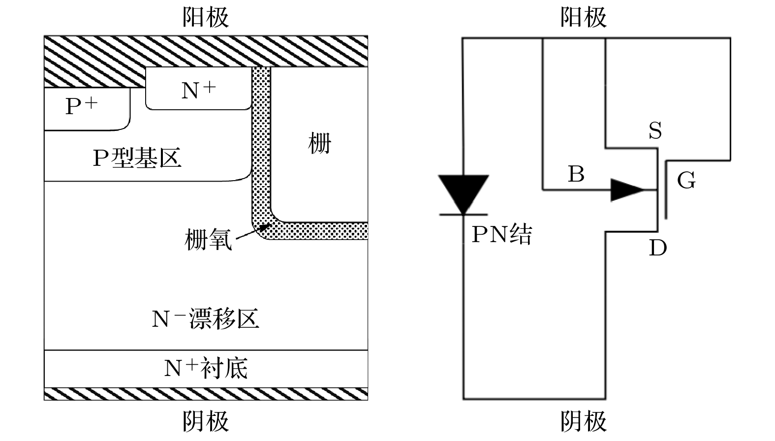 图 1 TSBR结构及原理图(G, 栅极; S, 源极; D, 漏极)
 图 2 耗尽区和关键点示意图
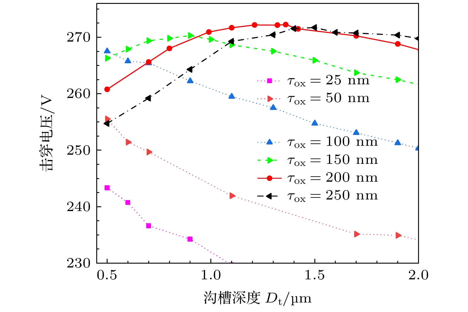 图 3 不同τox条件下击穿电压随Dt的变化趋势
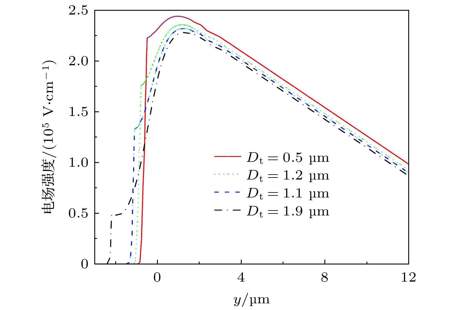 图 4 薄栅氧条件下Dt对台面中心电场分布的影响
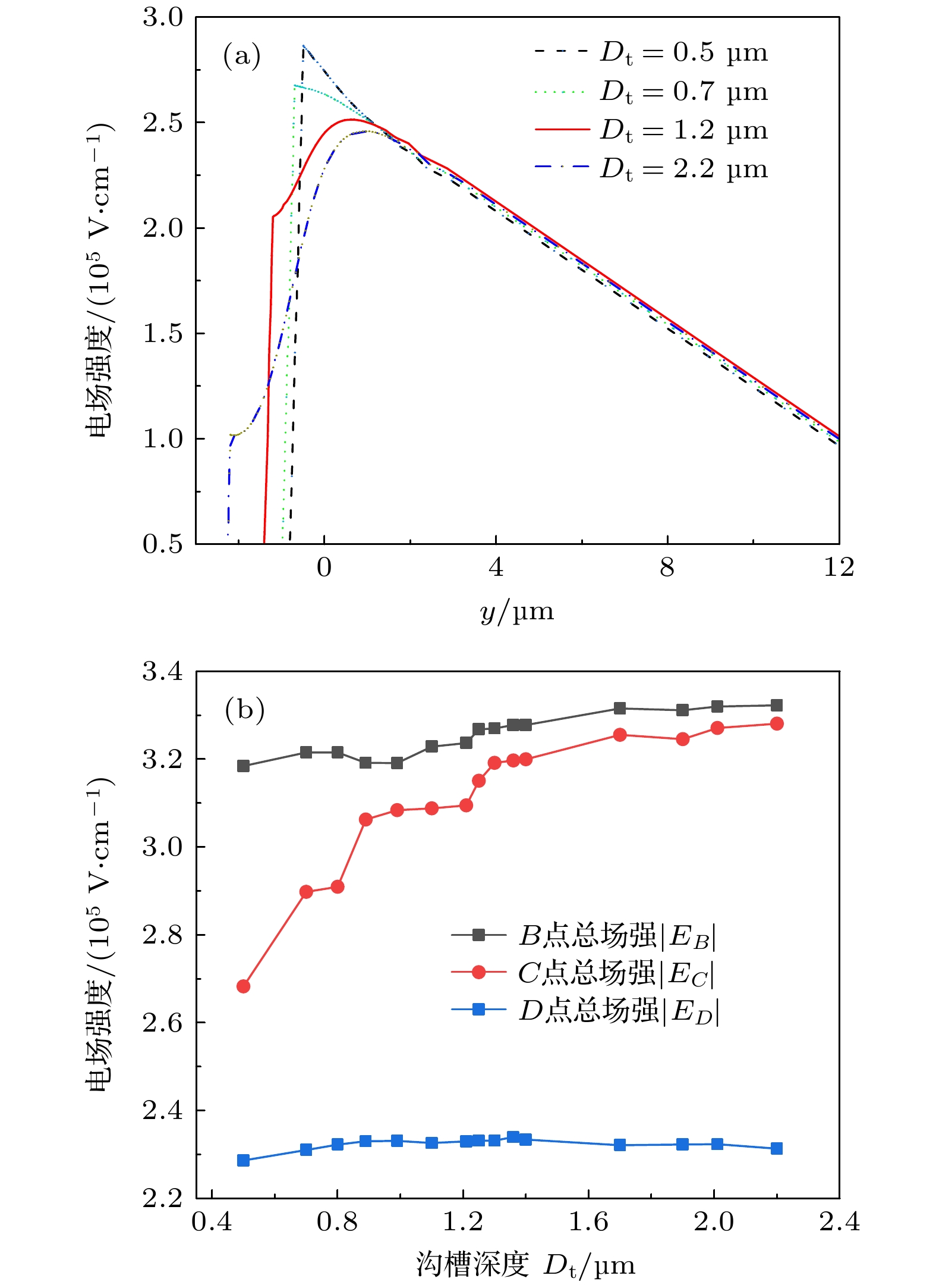 图 5 τox = 200 nm时Dt对台面中心电场分布(a)以及关键点场强(b)的影响
 图 6 Wms对台面中心电场分布的影响
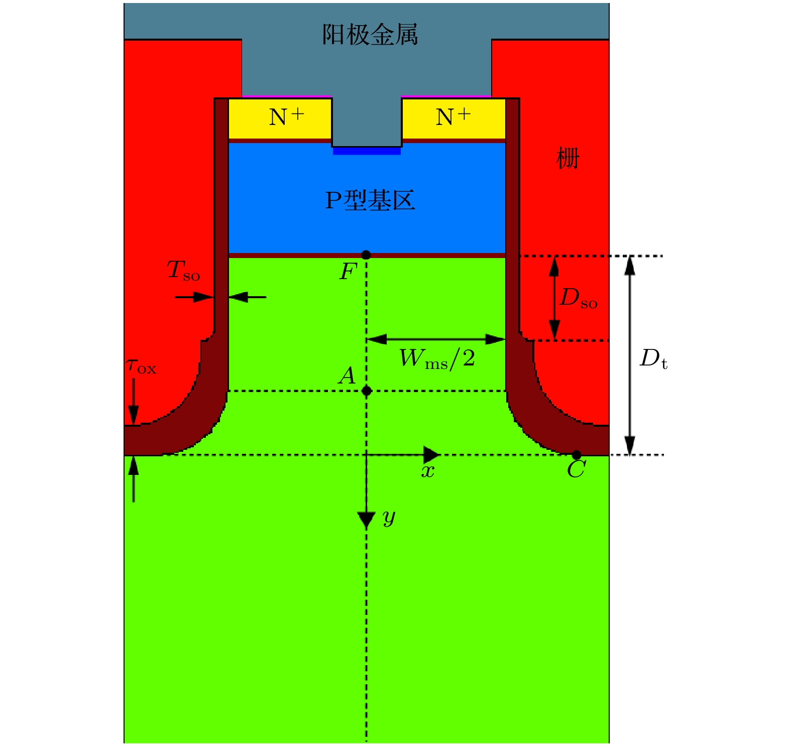 图 7 SO-TSBR结构图
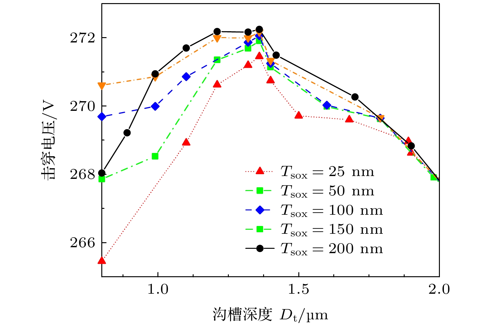 图 8 不同Tso条件下SO-TSBR击穿电压随Dt的变化
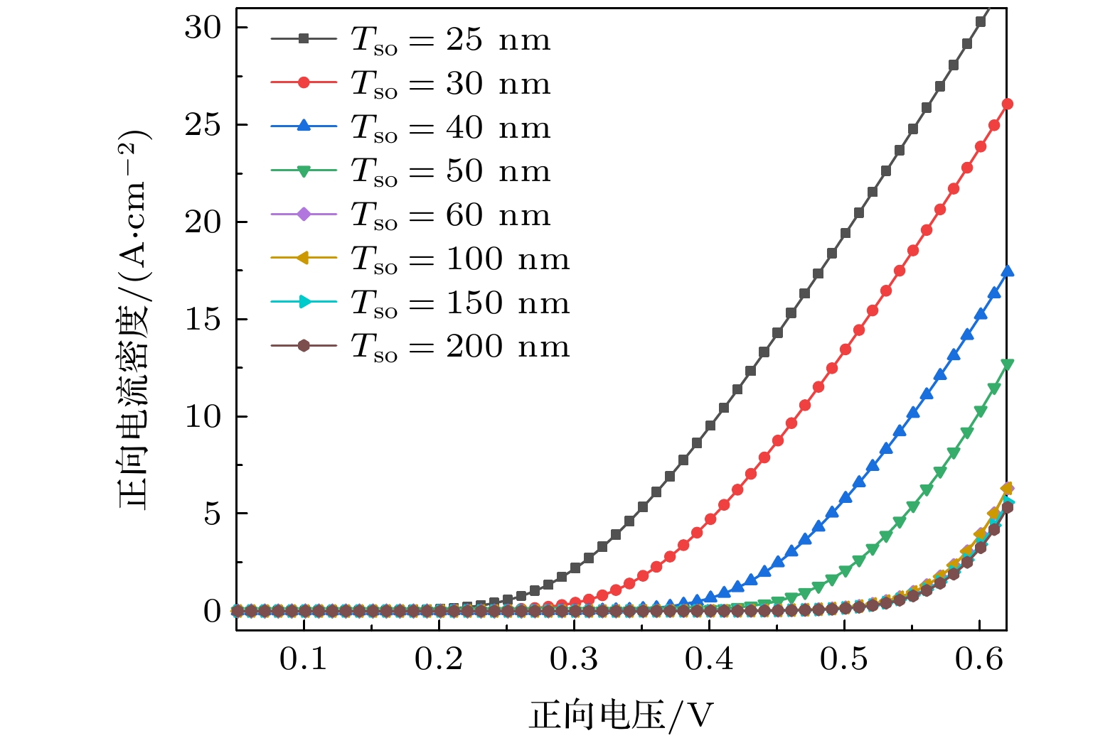 图 9 Tso对正向导通特性的影响
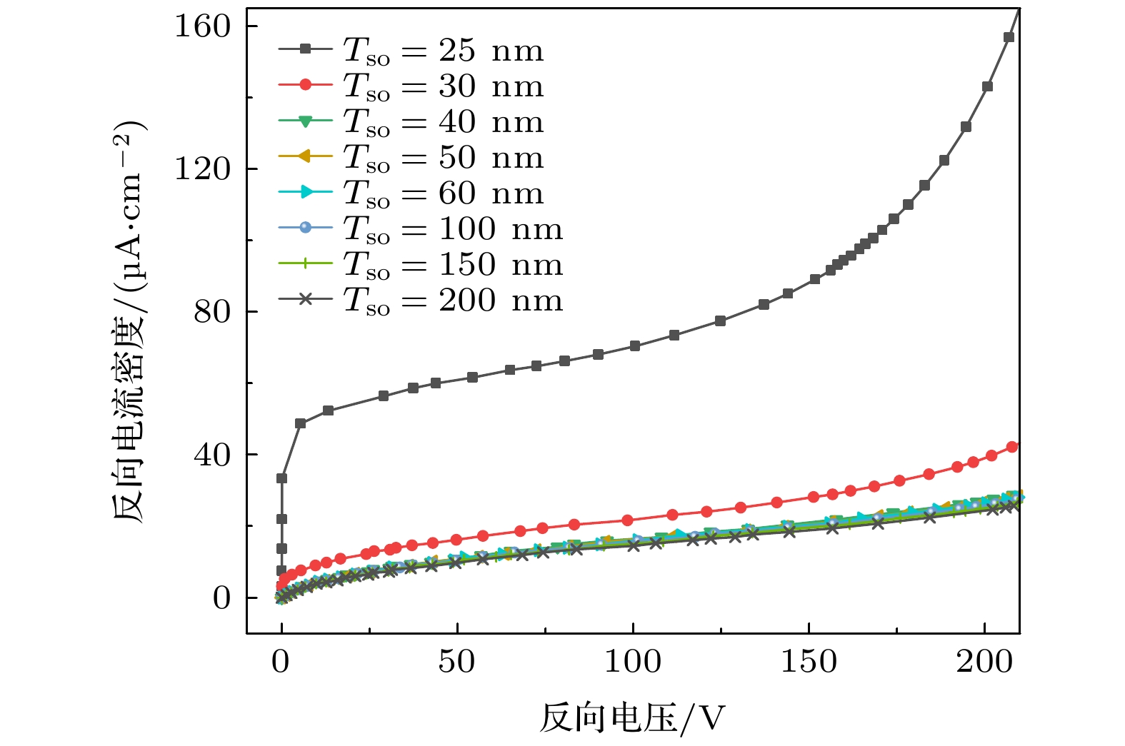 图 10 Tso对反向漏电流的影响