全文HTML
--> --> -->随着太阳能光伏器件设计对材料性能需求的发展, 异质结工程作为一种改善半导体材料光电性能的有效方法, 在实验和理论上得到了广泛的研究[15-29]. 二维层状晶体材料范德瓦耳斯(vdW)异质结[15-19]是通过将不同的二维材料叠加, 得到的垂直异质结的组装体, 它通常可以结合各组分固有的光电特性, 综合优化材料性能. 如二维/三维钙钛矿[1], 磷烯/石墨烯[20], MoS2/WS2[21], WS2/石墨烯[22], 钙钛矿/硅烯[23], CsPbI3/SnS[24], CsPbI3/BP[25,26]和CsPbBr3/PbSe [27]等诸多vdW异质结都被成功制备, 并表现出良好的光电性能. 比如, 张清林教授课题组[27]通过可控外延生长制备了CsPbBr3/PbSe异质结, 基于异质结的光电探测器在405 nm光照下表现出高达4.7 × 10⁴ A/W的光电流响应率. 黄楚云教授团队[28]在理论上表明石墨烯的Dirac锥和CH3NH3PbI3的直接带隙保留在石墨烯/CH3NH3PbI3异质结中, 石墨烯有望成为钙钛矿太阳能电池的支撑层. 冯宏剑教授团队[29]指出Graphene/CH3NH3PbI3异质结构可形成新的p-i-n结构钙钛矿太阳能电池, 他们还研究了较多钙钛矿范德瓦耳斯异质结(CsPbI3/SnS, CsPbI3/BP)的界面效应和光电性质[24,26]. 目前, 相关研究工作都表明钙钛矿和二维材料的异质结在光伏器件中具有巨大的研究和应用前景. 我们之前的理论研究发现, 2D-3D钙钛矿异质结的光吸收系数高于纯钙钛矿[1], 不同的界面接触改变了电子和空穴的复合, 影响了钙钛矿的PCE. 这些结果表明, 异质结的构建是提高二维材料光电性能和光伏器件稳定性及PCE的有效方法.
五环石墨烯(PG)是sp2和sp3两种杂化碳原子共存的新型全碳层状结构材料. 北京大学张顺洪博士等[30]在2015年理论预测PG能从T12碳中剥离出, 并通过能量稳定性、热稳定性和机械稳定性等方面的计算表明其具有良好的结构稳定性. 自从PG被提出后, 国际上许多著名研究组先后对PG结构[30-36]和类五环结构penta-P2C, P2Si[37], PdP2, PdAs2[38], PdSe2[39]和ZnO2[40]等开展了探索研究, 如刘艳平教授等[39]通过实验和理论合作测得penta-PdSe2表现出显著的各向异性响应吸收比: αy/αx在364 nm约为1.11, 532.00 nm约为1.15, 633.00 nm约为0.84, 具有很强的本征线性二色性效应. PG是一种准直接带隙半导体, 具有合适且可调的宽带隙, 独特的结构构型和优良的半导体特性, 有望在光电领域取得突破性应用. 但PG也存在很多问题, 其中亟待解决的就是本征PG的吸收光谱范围不佳. 通过PG与CsPbX3构建vdW异质结, 可以充分利用CsPbX3良好的光吸收性和量子转化效率; 同时, 无机层PG覆盖钙钛矿能有效提高钙钛矿材料的稳定性[10]. 因此, CsPbX3-PG异质结预期在光电性能应用方面具有令人期待的表现.
为了研究钙钛矿材料的稳定性, 充分利用其优越的光吸收性能和量子转化效率, 并进一步研究PG潜在的光电性能, 本文构建了全无机金属卤化物钙钛矿CsPbX3 (X = Cl, Br, I)和PG的vdW异质结, 通过密度泛函计算研究其半导体异质结的界面特性, 并选取较稳定的Pb-X界面的CsPbX3-PG (X = Cl, Br, I)异质结, 研究了其电子结构、界面电荷转移、动力学稳定性、光吸收率和太阳能功率转换效率等性质, 并从理论上探讨两种界面的稳定性和卤素原子X = Cl, Br, I对异质结电子结构调控的物理机制, 为基于CsPbX3-PG光伏器件的结构设计提供理论研究参考.
3.1.结构模型和稳定性
计算得到立方块体钙钛矿CsPbCl3, CsPbBr3, CsPbI3的晶格常数分别为a = b = c = 5.733 ?, a = b = c = 5.993 ?, a = b = c = 6.417 ?, PG单胞的晶格常数为a = b = 3.64 ?. 异质结中CsPbX3为四层八面体结构, 其性能与立方块体CsPbX3相似, 且四层CsPbX3和单层PG构成vdW异质结时旋转角度为26.57°. 在CsPbX3-PG异质结中, 由于CsPbX3具有两种不同的界面(Pb-X界面和Cs-X界面), CsPbX3可以通过不同界面与PG进行界面接触, 通过计算最小化表面结合能, 可以选择更稳定、更合理的异质结. 计算界面形成能公式为


| X | 晶格失配度/% | 界面形成能/(meV·?–2) | |
| PbX-PG | CsX-PG | ||
| Cl | 0.15 | –1.92 | 12.42 |
| Br | 1.33 | –6.02 | 0.54 |
| I | 3.46 | –5.43 | 1.03 |
表1CsPbX3-PG异质结的晶格失配度和表面结合能
Table1.Lattice mismatch ratio and surface binding energyof PbX and CsX interface in CsPbX3-PG heterostructures.
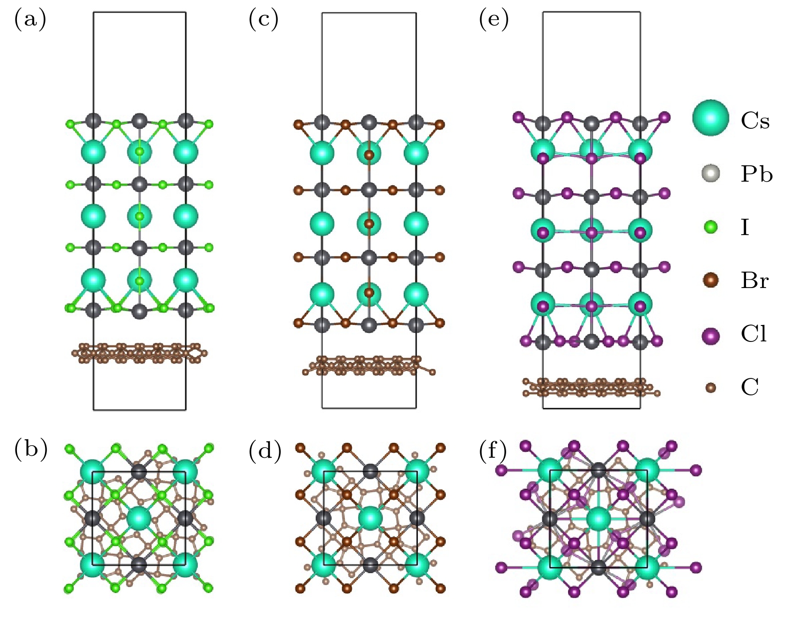 图 1 三种CsPbX3-PG异质结的顶部和侧面视图 (a), (b) CsPbCl3-PG; (c), (d) CsPbBr3-PG; (e), (f) CsPbI3-PG
Figure1. Top and side views of the CsPbX3-PG heterostructure: (a), (b) CsPbCl3-PG; (c), (d) CsPbBr3-PG; (e) (f) CsPbI3-PG.
为了验证CsPbX3-PG在室温下的动力学稳定性, 在正则系综(NVT)下进行了分子动力学(AIMD)模拟. 温度和能量随着模拟时间的变化如图2所示, 在5000 fs时间内, 这三个异质结能量变化极小, 温度振荡也很小并具有周期性变化, 表明研究的CsPbX3-PG体系满足动力学稳定性和热稳定性.
 图 2 分析动力学(AIMD)模拟, 能量和温度在300 K的相对于时间的波动 (a) CsPbCl3-PG异质结; (b) CsPbBr3-PG异质结; (c) CsPbI3-PG异质结
Figure2. Energy and temperature fluctuation respect to time in AIMD simulation at 300 K: (a) CsPbCl3-PG heterostructure; (b) CsPbBr3-PG heterostructure; (c) CsPbI3-PG heterostructure.
2
3.2.电子结构
电子能带结构对研究异质结的界面性质至关重要, 接下来分析CsPbX3-PG半导体异质结的电子结构性质. 图3(a)—图3(c)分别给出了计算的CsPbCl3-PG, CsPbBr3-PG, CsPbI3-PG异质结的能带结构图, 红线和蓝线分别表示PG单层和CsPbX3单层的能带结构图, 费米能级在图中设置为零. 结果表明, CsPbX3-PG异质结的电子能带结构基本可以看成是两种材料能带成分的组合, CsPbX3在接触状态下保持其直接带隙特性, PG单层保持其准直接带隙特性, 并且导带底(CBM)由PG贡献, 价带顶(VBM)由CsPbX3贡献, CsPbCl3-PG, CsPbBr3-PG和CsPbI3-PG异质结均为典型的Ⅱ型能带排列, 表明CsPbX3-PG异质结具有较好的光生载流子分离能力. 计算的单层PG, CsPbX3和PG-CsPbX3异质结的带隙如表2所列, 分别处于接触前状态和接触状态. 本文主要考虑的是异质结堆叠和界面相互作用的影响, 接触前后状态取的均是异质结中经晶格应变后的超胞状态, 结果显示两种状态下PG和CsPbX3带隙数值相差很小, 尤其是PG的带隙保持一致. 这说明层与层之间的相互作用非常弱, PG单层和CsPbX3在异质结中保持了单层的优异性能, PG改善了CsPbX3-PG的电子结构却不影响CsPbX3的本征特性.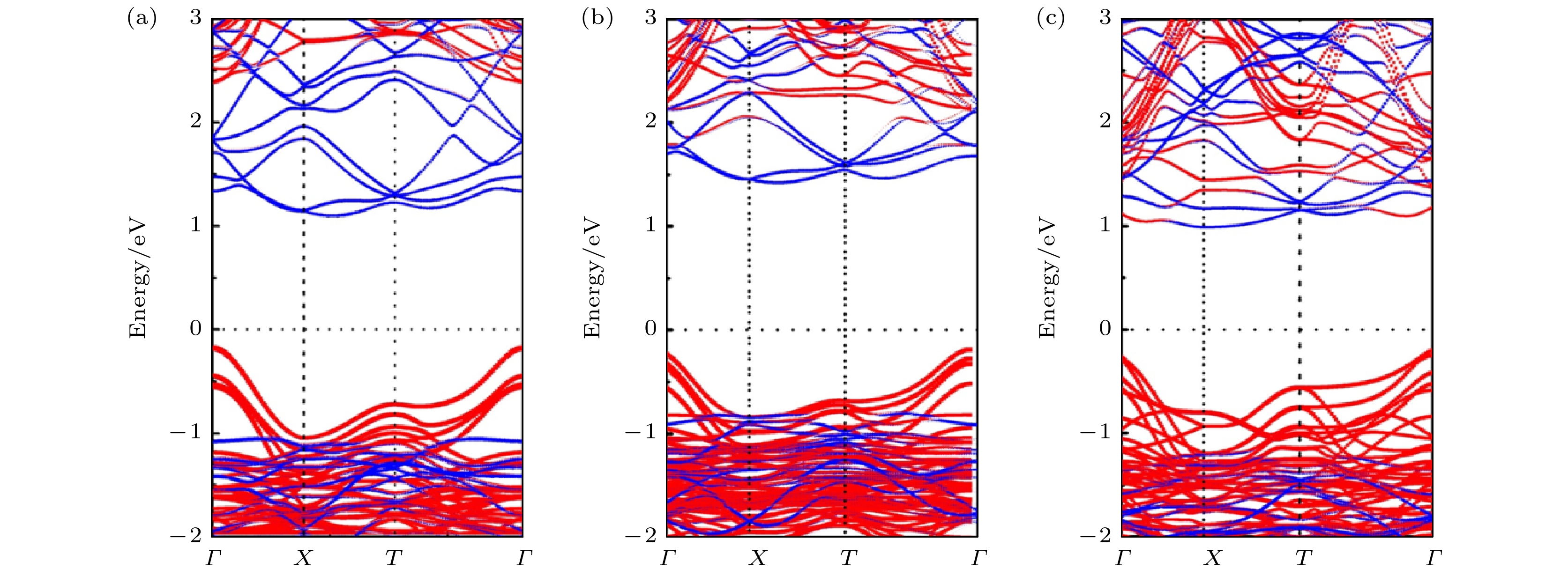 图 3 (a) CsPbCl3-PG, (b) CsPbBr3-PG, (c) CsPbI3-PG异质结的能带分解图, 红, 蓝线分别代表代CsPbX3和PG单层的能带
Figure3. Electronic band structures of heterostructures: (a) CsPbCl3-PG; (b) CsPbBr3-PG; (c) CsPbI3-PG. The red and blue lines represent the energy bands of CsPbX3 slabs and PG monolayer, respectively.
| X | 接触前(单结构) | 接触态(异质结) | ||||
| PG | CsPbX3 | PG | CsPbX3 | CsPbX3-PG | ||
| Cl | 2.21 | 2.21 | 2.21 | 2.62 | 1.30 | |
| Br | 2.28 | 1.77 | 2.28 | 1.79 | 1.62 | |
| I | 2.36 | 1.52 | 2.36 | 1.30 | 1.20 | |
表2CsPbX3-PG异质结接触前后带隙数据
Table2.Calculated band gaps of PG monolayer, CsPbX3 slabs and CsPbX3-PG heterostructures in the pre-contact state (left) and contact state (right) by PBE functional.
探索界面电荷转移对研究半导体异质结的界面性质具有重要意义. 图4中给出了CsPbX3-PG异质结构在接触前状态和接触状态下的能级排列图, 在未接触状态下, 真空能级(Ev)设置为零; 在接触状态下, 费米能级(Ef)设置为零. 图4显示了CsPbX3-PG异质结构能带类型均为II型排列, 表明CsPbX3-PG异质结构将具有较好的光生载流子分离能力. 对于CsPbX3体系, HSE06泛函预测的带隙明显高估, SOC预测的带隙则是会被低估, 而SOC对CsPbX3体系的带边可能会有较大影响[47-49], 因此在使用PBE计算能级排列的基础上, 再采用HSE + SOC测试了CsPbCl3-PG, CsPbBr3-PG, CsPbI3-PG异质结带边的能量本征值位置, 如图4(g)—图4(i)所示. 对比PBE的结果图4(d)—图4(f)可知, 两种方法计算的带隙值相差较小(CsPbCl3: 约0.3 eV, CsPbBr3: 约0.2 eV, CsPbI3: 约0.2 eV), 并且能带排列结果均为II型排列, 表明异质结具有较好的光生载流子分离能力.
 图 4 CsPbX3-PG异质结的能级排列图 (a)—(c)接触前, (d)—(f) PBE计算的接触状态, (g)—(i) HSE + SOC验证的接触状态下VBM和CBM点能量本征值. 其中, 蓝色块表示PG单层和红色块分别表示CsPbX3(X = Cl, Br, I)的能级
Figure4. The energy level alignment diagram of the CsPbX3-PG heterostructures: (a)–(c) the pre-contact states, (d)–(f) PBE calculated contact states and (g)–(i) HSE + SOC validated the energy eigenvalues of VBM and CBM points in the contact states. The blue blocks represent the energy level of PG monolayer and the red blocks represent the energy level of CsPbX3 slabs [X = Cl, Br, I (from left to right)].
为了阐明CsPbX3-PG异质结界面电荷转移的详细性质, 计算了异质结沿z方向的平面平均微分电荷密度ρ(z), 用于分析结构优化后异质结的界面耦合情况. CsPbX3-PG异质结界面电荷转移性质如图5(a)—图5(f)所示, 沿z轴的平面平均电荷密度差和三维电荷密度差可由如下公式计算[24]:
 图 5 沿Z方向上的平面平均差分电荷密度 (a) CsPbCl3-PG, (c) CsPbBr3-PG, (e) CsPbI3-PG异质结(红色区域为PG, 蓝色区域为CsPbX3); 3D差分电荷密度 (b) CsPbCl3-PG, (d) CsPbBr3-PG, (f) CsPbI3-PG异质结(黄色代表增益电子, 绿色代表损耗电子)
Figure5. The plane-averaged electron density difference along Z direction of (a) CsPbCl3-PG, (c) CsPbBr3-PG, (e) CsPbI3-PG. 3D charge density difference of heterostructures: (b) CsPbCl3-PG, (d) CsPbBr3-PG, (f) CsPbI3-PG. (Yellow represents gain electrons, and green represents lose electrons).


2
3.3.光电特性
研究异质结的光吸收能力对于其在光电器件中的应用具有重要意义. 吸收光谱是根据介电函数计算的:


图6给出了CsPbX3-PG异质结、单层PG和CsPbX3的光吸收谱, 异质结的光吸附峰边缘均位于可见光区域. 我们发现, 与CsPbX3和PG单层相比, CsPbCl3-PG异质结在红外, 可见光和紫外区域的光吸收率有明显提高, 高达4 × 105 cm–1, 其中PG的光学带隙小于CsPbCl3, 可见PG拓宽了异质结光吸收范围; CsPbBr3-PG异质结的光吸收率扩展到红外区域, 且可见光和紫外区域明显有提高, 高达5 × 105 cm–1, CsPbBr3的光学带隙比PG小; CsPbI3-PG异质结在可见光和紫外区域的光吸收率稍有提高, CsPbI3光学带隙明显小于PG, 光吸收率也高达5 × 105 cm–1. CsPbX3-PG异质结的光吸收系数强度和吸收范围都得到明显的改善. 此外, 光吸收谱范围主要取决于带隙, CsPbX3-PG异质结的光吸收谱范围相对于带隙较大的单层而言明显红移. 计算的光吸收谱表明, 通过构建异质结可以有效地调节PG单层的光吸收率和改善光吸收范围, CsPbX3-PG异质结具有很好的光吸收能力和光电器件应用潜力.
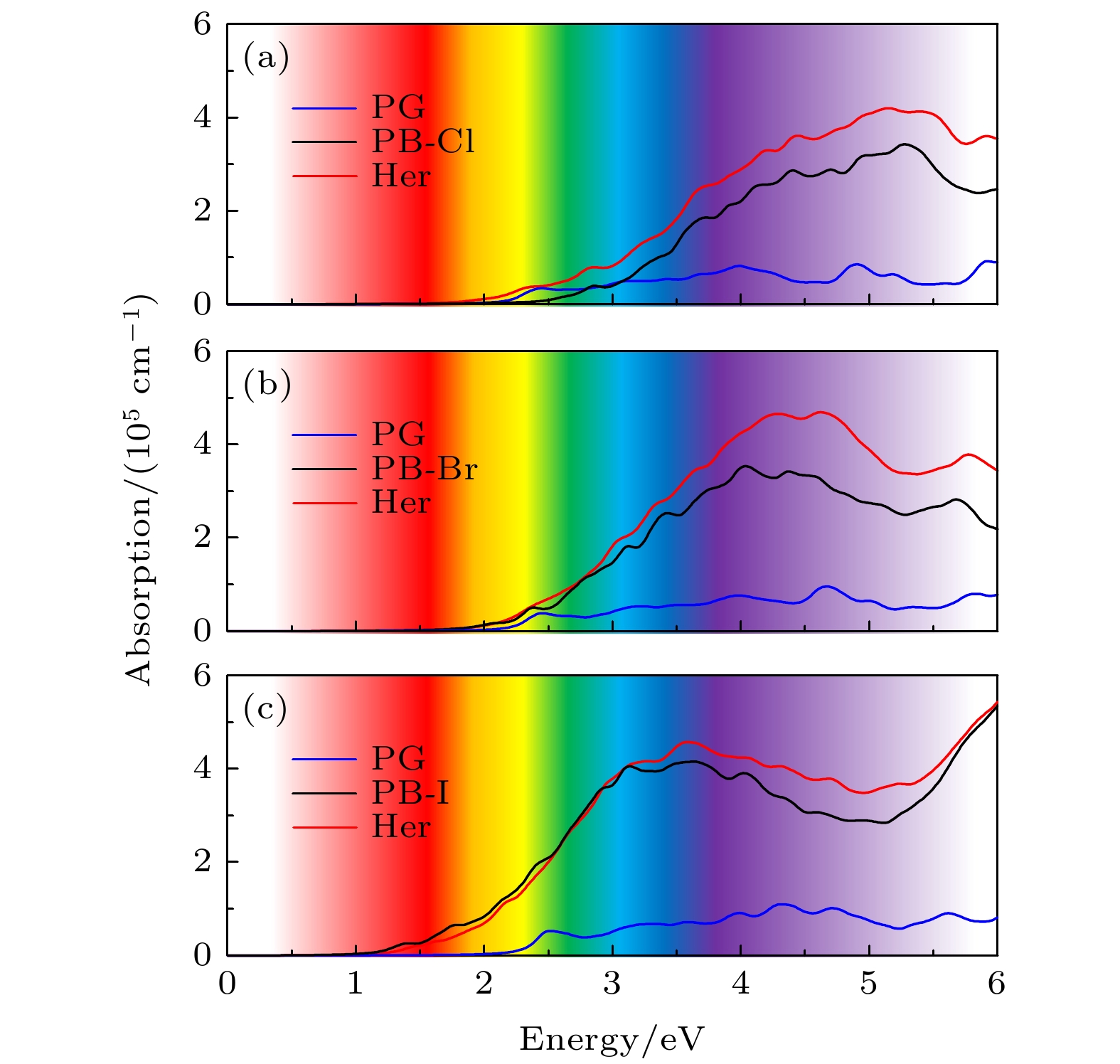 图 6 光吸收谱 (a) CsPbCl3-PG; (b) CsPbBr3-PG; (c) CsPbI3-PG异质结 (红线、蓝线和黑线分别代表CsPbX3-PG (X=Cl, Br, I)异质结、CsPbX3和PG单层的光吸收率 (X=Cl, Br, I)
Figure6. Light absorption capacity of (a) CsPbCl3-PG, (b) CsPbBr3-PG, (c) CsPbI3-PG. The red, blue and black line represent the light absorption capacity of CsPbX3-PG heterostructures, CsPbX3 slabs and PG monolayer, respectively [X=Cl, Br, I (up-down)].
此外, 对于II型能带排列的异质结, 按照Scharber等[52]的方法进一步估计它们的PCE, 其中PCE在100%外部量子效率极限中的上限可以表示如下:


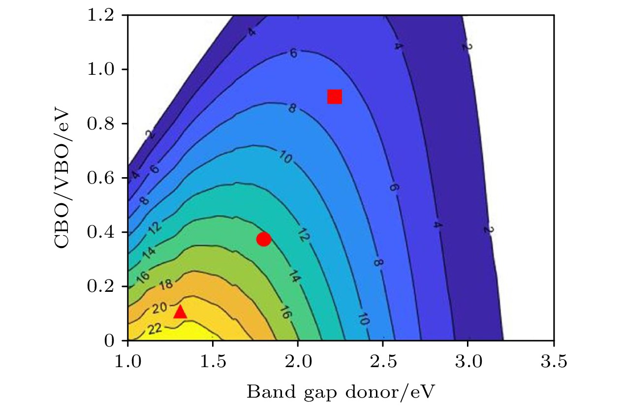 图 7 CsPbX3-PG(X=Cl, Br, I)异质结功率转换效率, 带隙和导带偏移的函数关系曲线. CsPbBr3-PG, 红色圆形; CsPbI3-PG: 红色三角形
Figure7. Power conversion efficiency contour plot as a function of the donor optical gap and conduction band offset ΔEC. Red circle and triangle represent CsPbBr3-PG and CsPbI3-PG, respectively.
图7给出了所有II型异质结的PCE等值线图. 光伏材料要求结构具有1.0—1.8 eV的合适光学带隙, 构建异质结可以有效地将带隙缩小到一个更合适的范围, 导致更高的PCE, CsPbX3-PG异质结的光学带隙分别取较小光学带隙值(供体)的单层, 其中CsPbCl3-PG取PG带隙值 2.21 eV, CsPbBr3-PG取CsPbBr3带隙值1.79 eV, CsPbI3-PG取CsPbI3带隙值1.30 eV. 此外, 通过减少CBO/VBO可以改善PCE, 其中CsPbCl3-PG取VBO值为1.28 eV, CsPbBr3-PG和CsPbI3-PG取CBO值分别为0.24 和0.11 eV, 并结合CBO和带隙值可在AM1.5光谱的PCE等高线上分别估算出CsPbCl3-PG, CsPbBr3-PG和CsPbI3-PG的PCE约为7%, 15%和21%.
