1.College of Electric and Mechanical Engineering, Pingdingshan University, Pingdingshan 467000, China 2.College of Physics, Henan Normal University, Xinxiang 453007, China 3.School of Mathematics and Physics, Henan University of Urban Construction, Pingdingshan 467036, China
Abstract:The contacts between semiconductor and metal are vital in the fabrication of nano electronic and optoelectronic devices. The contact type has a great influence on the function realization and performance of the device. In order to prepare multifunctional devices with high performance, it is necessary to modulate the barrier height and contact type at the interface. First-principles calculations based on the density functional theory (DFT) are implemented in the VASP package. The generalized gradient approximation of Perdew, Burke, and Ernzerhof (GGA-PBE) with van der Waals (vdW) correction proposed by Grimme (DFT-D3) is chosen due to its good description of long-range vdW interactions. It is demonstrated that weak vdW interactions dominate between graphene and InSe with their intrinsic electronic properties preserved. We find that the n-type ohmic contact is formed at the graphene/InSe interface with the Fermi level through the conduction band of InSe (ΦBn < 0). The Fermi level of graphene/InSe heterostructure moves down to below the Dirac point of graphene layer, which results in p-type (hole) doping in graphene. Moreover, the external electric field is effective to tune the Schottky barrier, which can control not only the Schottky barrier height but also the type of contact. With the negative external electric field varying from 0 to –1 V/nm, the conduction band minimum of InSe below the Fermi level declines gradually but the n-type ohmic contact is still preserved. Nevertheless, with the positive external electric field varying from 0 to 0.8 V/nm, the conduction band minimum of InSe shifts upward and across the Fermi level, the conduction band minimum of InSe is closer to the Fermi level than the valence band maximum, which indicates that the n-type Schottky contact is formed. The Fermi level moves from the the conduction band minimum to the valence band maximum of InSe when the positive external electric field increases from 0.8 V/nm to 2 V/nm. The n-type Schottky barrier height exceeds the p-type Schottky barrier height gradually, which demonstrates that the positive external electric field transforms the n-type Schottky contact into the p-type Schottky contact at the graphene/InSe interface. When the positive external electric field exceeds 2 V/nm, the valence band of InSe moves upward and cross the Fermi level (ΦBp < 0), the ohmic contact is obtained again. Meanwhile, p-type (hole) doping in graphene is enhanced under negative external electric field and a large positive external electric field is required to achieve n-type (electron) doping in graphene. The external electric field can control not only the amount of charge transfer but also the direction of charge transfer at the graphene/InSe interface. Keywords:Schottky barrier/ electric field/ graphene/InSe van der Waals heterostructure
为了能够更好地构建graphene/InSe异质结, 首先计算了graphene和InSe单层的结构参数, graphene和InSe两者都为六角晶格结构, 优化后的graphene和InSe的晶格常数分别为2.46 ?和4.09 ?, 与以前的研究结果相符合[39,40]. 为了使异质结的晶格失配最小, 采用${\sqrt 3}\! \times \! {\sqrt 3 } \! \times \! 1$ 的graphene晶胞和1 × 1 × 1的InSe晶胞构建异质结, 二者的失配度为4.2%. 图2 为graphene/InSe异质结优化后的顶视图和侧视图. 计算结果表明优化后graphene/InSe异质结中graphene和InSe单层的层间距为3.51 ?, 此间距远大于C原子和Se原子的共价半径之和, 与graphene/MoS2[18], graphene/WSe2[41]等范德瓦耳斯异质结的层间距接近, 这就表明graphene与InSe之间为微弱的范德瓦耳斯作用. 为了表征graphene/InSe异质结的稳定性, 计算了异质结的束缚能, 表达式为Eb = (Ehetero – Egraphene –EInSe)/N, 其中Ehetero, Egraphene和EInSe分别为graphene/InSe异质结、graphene和单层InSe的总能, N = 6为异质结超原胞中包含的C原子数. 计算结果表明, graphene/InSe异质结的束缚能为–106.4 meV, 束缚能为负意味着异质结可稳定存在, 束缚能的大小与graphene/MoS2[18], graphene/WSe2[41]等范德瓦耳斯异质结的束缚能比较接近, 再次验证了异质结中graphene和InSe之间为微弱的范德瓦耳斯作用. 图 2 (a) Graphene/InSe异质结的顶视图; (b) graphene/InSe异质结的顶视图; 灰色、橙色和棕色小球分别表示碳原子、硒原子和铟原子 Figure2. Top view (a) and side view (b) of the graphene/InSe heterostructures. The gray, orange and brown balls are for C, Se and In atoms, respectively.
23.2.Graphene/InSe异质结的电子结构 -->
3.2.Graphene/InSe异质结的电子结构
为了系统研究graphene/InSe异质结的电子性质, 图3给出了graphene/InSe异质结的投影能带结构图、graphene的能带结构图和单层InSe的能带结构图. 由图3(b)可以看出, graphene为零带隙, 费米能级恰好穿过高对称的狄拉克点. 与通常graphene的狄拉克点位于K点不同, 图3(b)中的狄拉克点是位于Γ点的, 对于$\sqrt 3 $ × $\sqrt 3 $ × 1的graphene晶胞, 晶胞的扩大将导致能带发生折叠, 这使得K点与Γ点重合, 从而导致graphene的狄拉克点位于Γ点. 从图3(c)可以看出, 单层的InSe为间接带隙半导体, 导带底位于Γ点, 价带顶则位于K点与Γ点之间, 带隙宽度为1.55 eV. 将graphene/InSe异质结的能带结构与graphene和单层InSe的能带结构进行比较后发现, graphene/ InSe异质结的能带基本上就是组成异质结的graphene和单层InSe能带的简单迭加, 组成异质结的graphene和单层InSe很大程度上保留了各自独立的电子结构, 两者的能带形状几乎没有发生改变. Graphene依旧表现出半金属特性而单层InSe则仍为间接带隙. 这进一步印证了异质结中graphene和InSe之间为微弱的范德瓦耳斯作用. 组成异质结前, graphene的狄拉克点位于费米能级处, 形成异质结后, 费米能级移动到狄拉克点的下方, 这使得graphene层变为p型掺杂, 费米能级相对狄拉克点下移表明在形成graphene/InSe异质结的过程中graphene层失去了电子. 图3(c)显示单层InSe为p型半导体, 形成异质结后由图3(a)可以看出费米能级穿过了单层InSe的导带, 费米能级位于单层InSe导带底的上方, 电子由graphene层转移到了InSe层, 并最终在异质结中形成了内建电场, 方向由graphene指向InSe. Graphene/InSe是典型的金属-半导体异质结, 从半导体器件应用的观点来看, graphene可作为金属电极而单层InSe则作为沟道材料, 由肖特基-莫特模型[22]可知, n型肖特基势垒ΦBn = EC – EF, EC为单层InSe的导带底, EF为graphene/InSe异质结的费米能级, 由图3(a)得出ΦBn = –0.05 eV, ΦBn < 0意味着在graphene和InSe界面形成了n型欧姆接触. 图 3 (a) Graphene/InSe异质结的投影能带结构图, 红色线条表示graphene的能带, 蓝色线条表示InSe的能带; (b) graphene的能带结构图; (c)单层InSe的能带结构图; 费米能级设为零点 Figure3. (a) Projected band structure of the graphene/InSe heterostructure, where the red and blue lines represent for the energy band of graphene and InSe, respectively; (b) the band structure of graphene; (c) the band structure of monolayer InSe. The Fermi level is set to zero.
${\rho _{{\rm{graphene/InSe}}}}$(x, y, z), ${\rho _{{\rm{graphene}}}}$(x, y, z)和${\rho _{{\rm{InSe}}}}$(x, y, z)分别表示graphene/InSe异质结、graphene和单层InSe在(x, y, z)点的电荷密度. 因此图4中的正值表示电荷增加, 负值表示电荷减少. 由图4可以看出, graphene和InSe形成异质结后graphene层的电子减少, InSe层的电子增加, 这就表明电子是由graphene层转移到了InSe层, 而空穴则由InSe层转移到了graphene层. 电荷在graphene/InSe异质结的界面进行了重新分布, 电荷的重新分布导致了界面附近电子-空穴对和内建电场的产生. 图 4 Graphene/InSe异质结的平面平均差分电荷密度图, 图中的竖直黑色虚线表示graphene层和InSe层的分界线 Figure4. Plane-averaged charge density difference of the graphene/InSe heterostructure. The black vertical dashed line denotes the intermediate position of graphene and InSe.
23.3.外加电场对graphene/InSe异质结电子结构的调控 -->
3.3.外加电场对graphene/InSe异质结电子结构的调控
Graphene/InSe异质结在纳电子器件如场效应管领域有潜在的应用, 当基于graphene/InSe异质结的场效应管工作时, graphene/InSe就处于外加电场中, 外加电场对graphene/InSe异质结电子性质的影响至关重要. 因此本文研究了外加电场对graphene/InSe异质结电子结构的调控, 外加电场的正方向由graphene指向InSe, 与内建电场的方向相同. 图5给出了施加不同外电场时graphene/InSe异质结的投影能带图. 对graphene/InSe异质结施加负方向的外电场时, 电子由graphene转移到了InSe, InSe的导带底依然位于费米能级下方, 并相对于费米能级持续下降, n型肖特基势垒ΦBn始终小于0, 因此施加负方向的外电场时graphene与InSe的界面始终为n型欧姆接触. 当施加正方向的外电场时, InSe的导带底相对于费米能级逐渐上升, 导带底移动到了费米能级的上方, n型肖特基势垒ΦBn大于0, 并且ΦBn < ΦBp, 这就表明graphene与InSe的界面由n型欧姆接触转变为n型肖特基接触. 正方向的外电场进一步增加时, InSe的导带底和价带顶相对于费米能级持续上升, 导致ΦBn > ΦBp, 此时graphene与InSe的界面就由n型肖特基接触转变为了p型肖特基接触. 随后正方向的外电场持续增加, InSe的价带顶相对于费米能级进一步上升, p型肖特基势垒ΦBp持续减小, 最终价带顶移动到了费米能级的上方, p型肖特基势垒ΦBp减小为0并进一步减小变为负值, graphene与InSe的界面由p型肖特基接触转变为了p型欧姆接触. 由图5可以看出, 当没有施加外加电场时, 费米能级位于狄拉克点的下方, 两者之间的能量差值为0.08 eV, graphene层为p型掺杂. 而当施加负方向的外加电场时, 更多的电子由graphene层转移到了InSe层, 狄拉克点相对于费米能级上移, 在外加电场为–0.5和–1 V/nm时, 狄拉克点和费米能级间的能量差值分别为0.13和0.27 eV, 随着负方向外电场的增加, graphene层的p型掺杂增强了. 而正方向的外电场使得电子由InSe转移到了graphene, 狄拉克点移动到了费米能级的下方, graphene层由p型掺杂变为n型掺杂, 正方向的外电场越大, graphene层的n型掺杂越强. 图 5 施加不同外电场时graphene/InSe异质结的投影能带图, 图中蓝色线条表示InSe的能带, 红色线条表示graphene的能带, 费米能级设为零点 Figure5. Projected band structures of graphene/InSe heterostructures under different external electric fields. The red and blue lines represent for the energy band of graphene and InSe, respectively. The Fermi level is set to zero.
为了定量描述外电场对graphene/InSe异质结肖特基势垒的调控, 图6给出了graphene/InSe异质结的肖特基势垒随外加电场的变化关系图. 对异质结施加正方向的外加电场后, 电子由InSe向graphene转移, InSe的导带底和价带顶相对于费米能级上移, 导带底移动到费米能级上方, n型肖特基势垒ΦBn就由负值变为正值, graphene和InSe的界面就由n型欧姆接触转变为了肖特基接触, 由于ΦBn < ΦBp, 此接触为n型肖特基接触. 随着正方向外电场的增大, ΦBn持续增大, ΦBp持续减小, 当正方向的外电场达到0.8 V/nm时, ΦBn开始超过ΦBp, 此时界面的n型肖特基接触就转变为了p型肖特基接触. 当正方向的外加电场增加到2 V/nm时, 费米能级穿过InSe的价带顶, ΦBp减小为0并进一步变为负值, p型肖特基接触又转变为了p型欧姆接触. 对异质结施加负方向的外电场时, InSe的导带底和价带顶相对于费米能级下移, ΦBn始终小于0, 因此负方向的外电场不能改变界面的接触类型, graphene和InSe的界面在负电场作用下始终为n型欧姆接触. 图 6 Graphene/InSe异质结的肖特基势垒随外电场的变化 Figure6. Evolution of Schottky barriers of the graphene/InSe heterostructurer as a function of external electric field.
其中${\rho _E}(x, y, z)$和${\rho _{{\rm{graphene/InSe}}}}(x, y, z)$分别表示施加外电场和没有外电场时graphene/InSe异质结在(x, y, z)点的电荷密度. 计算结果表明正外电场和负外电场对graphene/InSe异质结界面的电荷转移影响不同. 如图7所示, 对异质结施加正外电场时, graphene得到了电子而InSe失去了电子, 费米能级向下移动, 由最初位于InSe导带底的上方移动到了InSe价带底的下方, 界面在这个过程中实现了由n型欧姆接触到n型肖特基接触再到p型肖特基接触最终变为p型欧姆接触的转变, graphene层的n型掺杂增强. 而在负外电场作用下, 电子由graphene转移到了InSe, 费米能级向上移动, 逐渐远离InSe的导带底, 界面始终为n型欧姆接触, graphene层的n型掺杂增强. 电荷转移的数量随着外加电场的增大逐渐增加, 但与外加电场的方向无关. Graphene和InSe之间逐渐增加的电荷转移意味着二者的相互作用进一步加强, 并导致了异质结中费米能级的移动. 因此, 界面电荷转移和费米能级的移动是外电场作用下异质结的接触类型转变的根本原因. 图 7 (a) 施加正外电场时graphene/InSe异质结的平面平均差分电荷密度图; (b) 施加负外电场时graphene/InSe异质结的平面平均差分电荷密度图; 图中的竖直黑色虚线表示graphene层和InSe层的分界线 Figure7. (a) Plane-averaged charge density difference of the graphene/InSe heterostructure under positive external electric fields; (b) the plane-averaged charge density difference of the graphene/InSe heterostructure under negative external electric fields. The black vertical dashed line denotes the intermediate position of graphene and InSe.
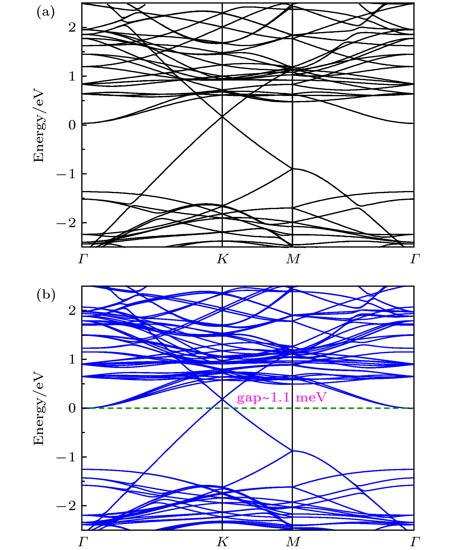 图 1 (a) 本文计算得到的graphene/MoS2异质结的能带结构图; (b) 文献[38]计算得到的graphene/MoS2异质结的能带结构图
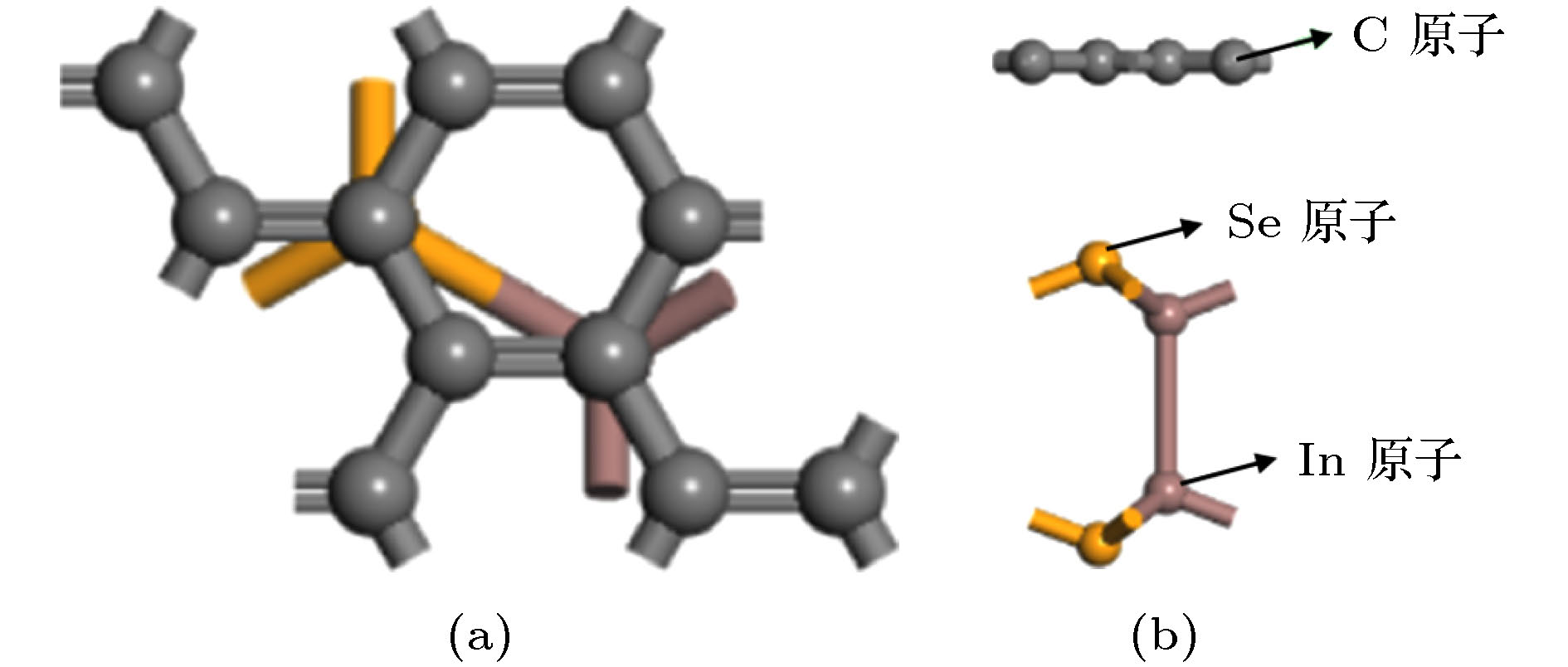 图 2 (a) Graphene/InSe异质结的顶视图; (b) graphene/InSe异质结的顶视图; 灰色、橙色和棕色小球分别表示碳原子、硒原子和铟原子

 图 3 (a) Graphene/InSe异质结的投影能带结构图, 红色线条表示graphene的能带, 蓝色线条表示InSe的能带; (b) graphene的能带结构图; (c)单层InSe的能带结构图; 费米能级设为零点


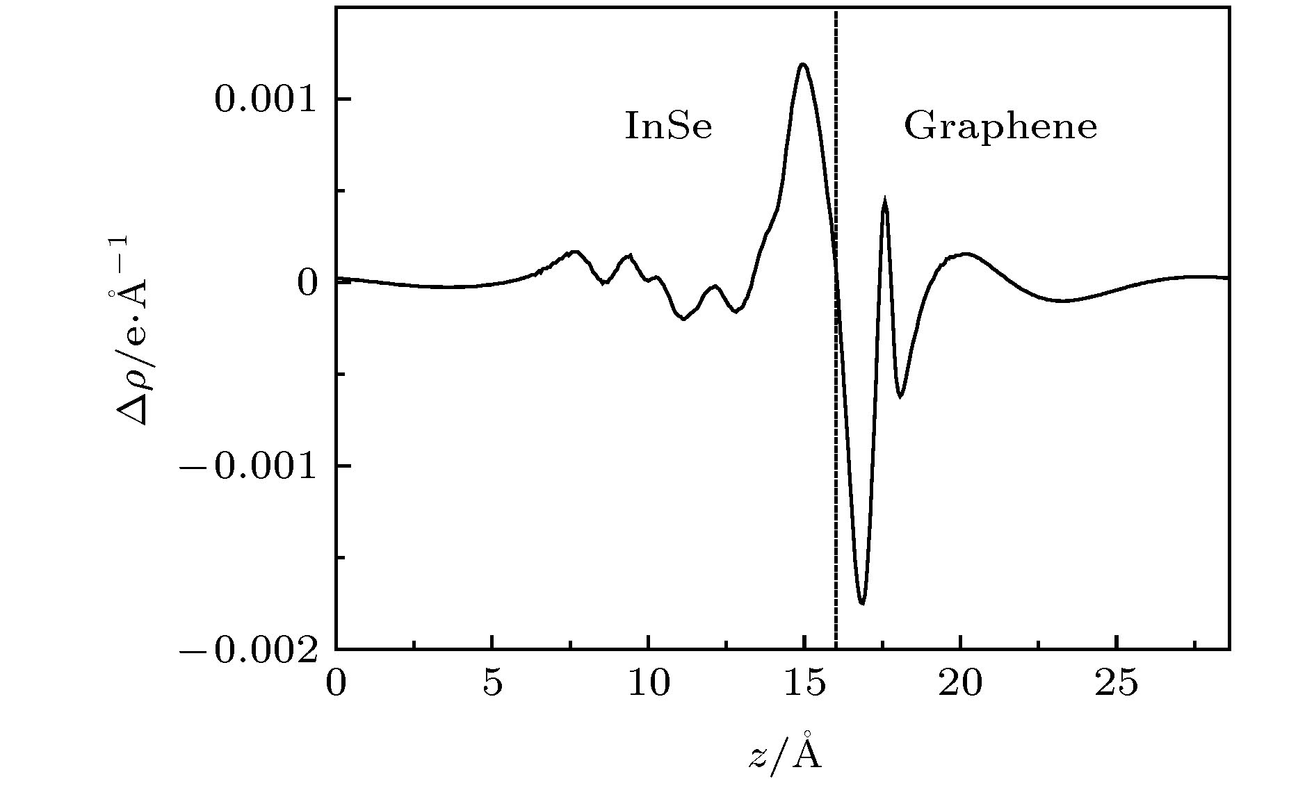 图 4 Graphene/InSe异质结的平面平均差分电荷密度图, 图中的竖直黑色虚线表示graphene层和InSe层的分界线
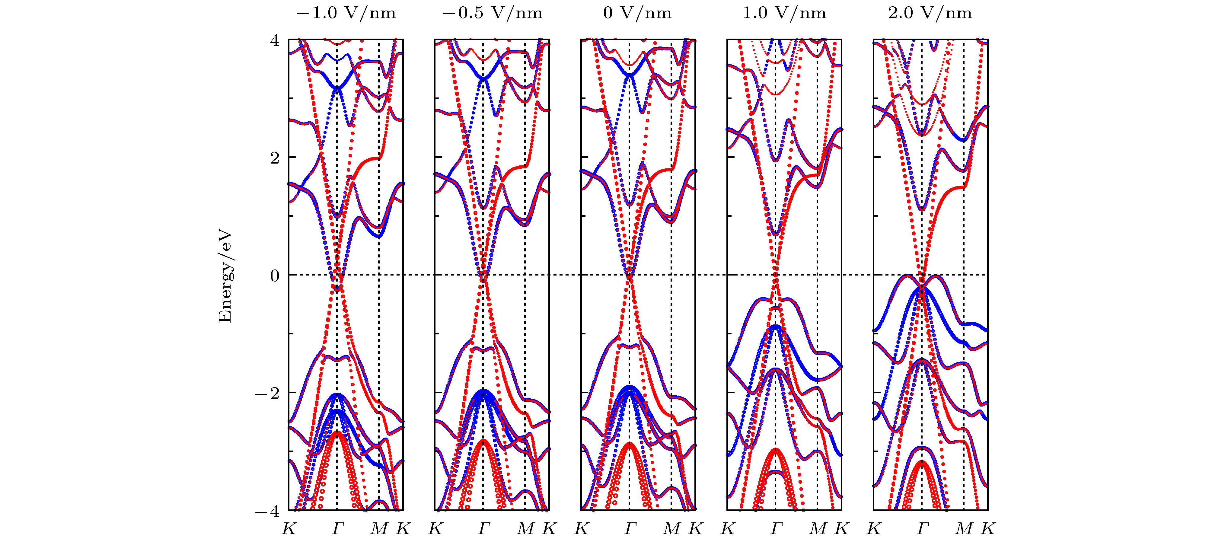 图 5 施加不同外电场时graphene/InSe异质结的投影能带图, 图中蓝色线条表示InSe的能带, 红色线条表示graphene的能带, 费米能级设为零点
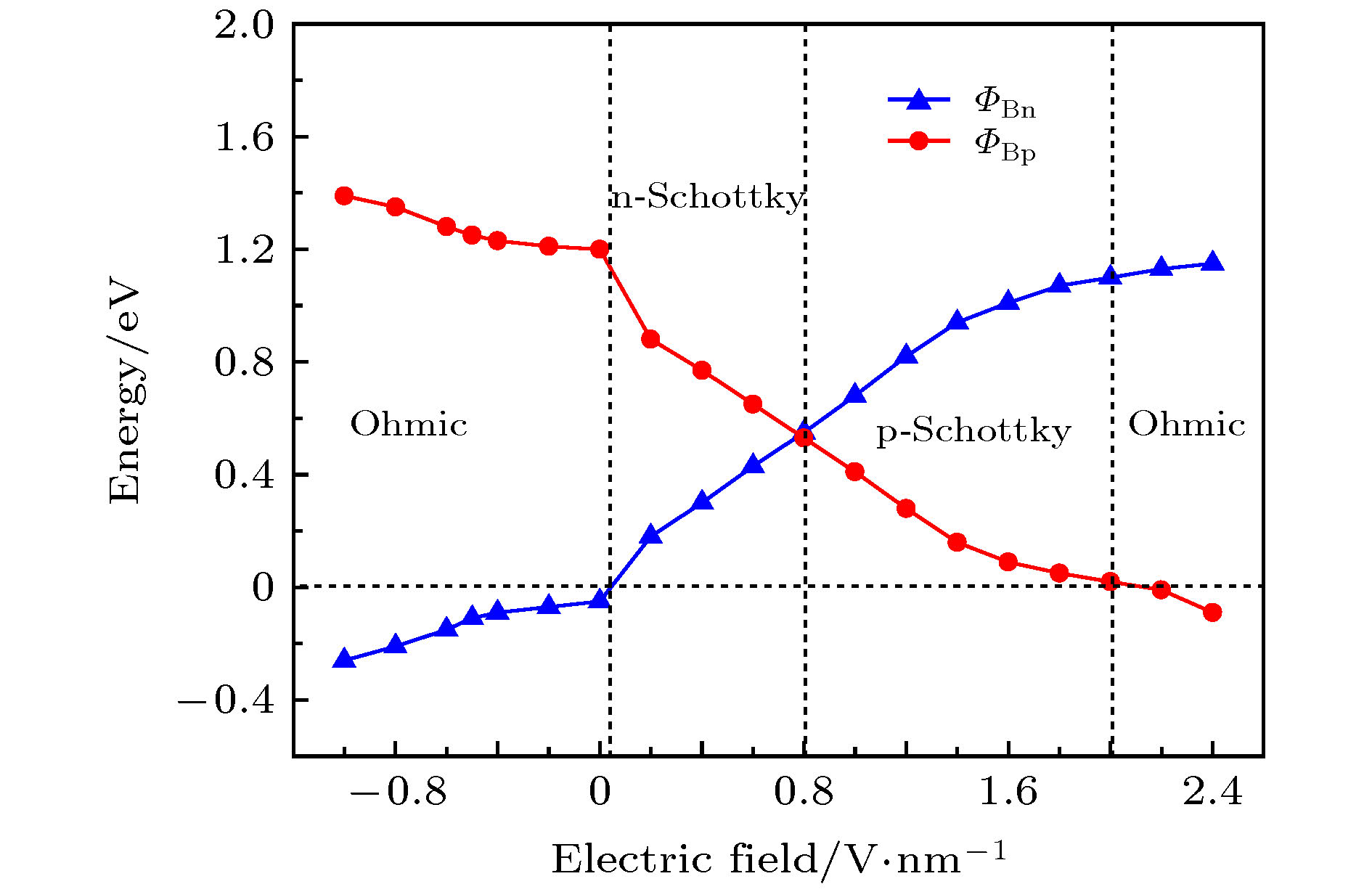 图 6 Graphene/InSe异质结的肖特基势垒随外电场的变化

 图 7 (a) 施加正外电场时graphene/InSe异质结的平面平均差分电荷密度图; (b) 施加负外电场时graphene/InSe异质结的平面平均差分电荷密度图; 图中的竖直黑色虚线表示graphene层和InSe层的分界线


