全文HTML
--> --> -->本文使用半导体仿真软件搭建了45 nm工艺HfO2基FeFET读写电路, 对其不同敏感节点进行了单粒子翻转效应研究, 分析了存储数据发生变化的内在机制, 这对航空电子器件结构的设计和抗单粒子电路的搭建具有重要意义.
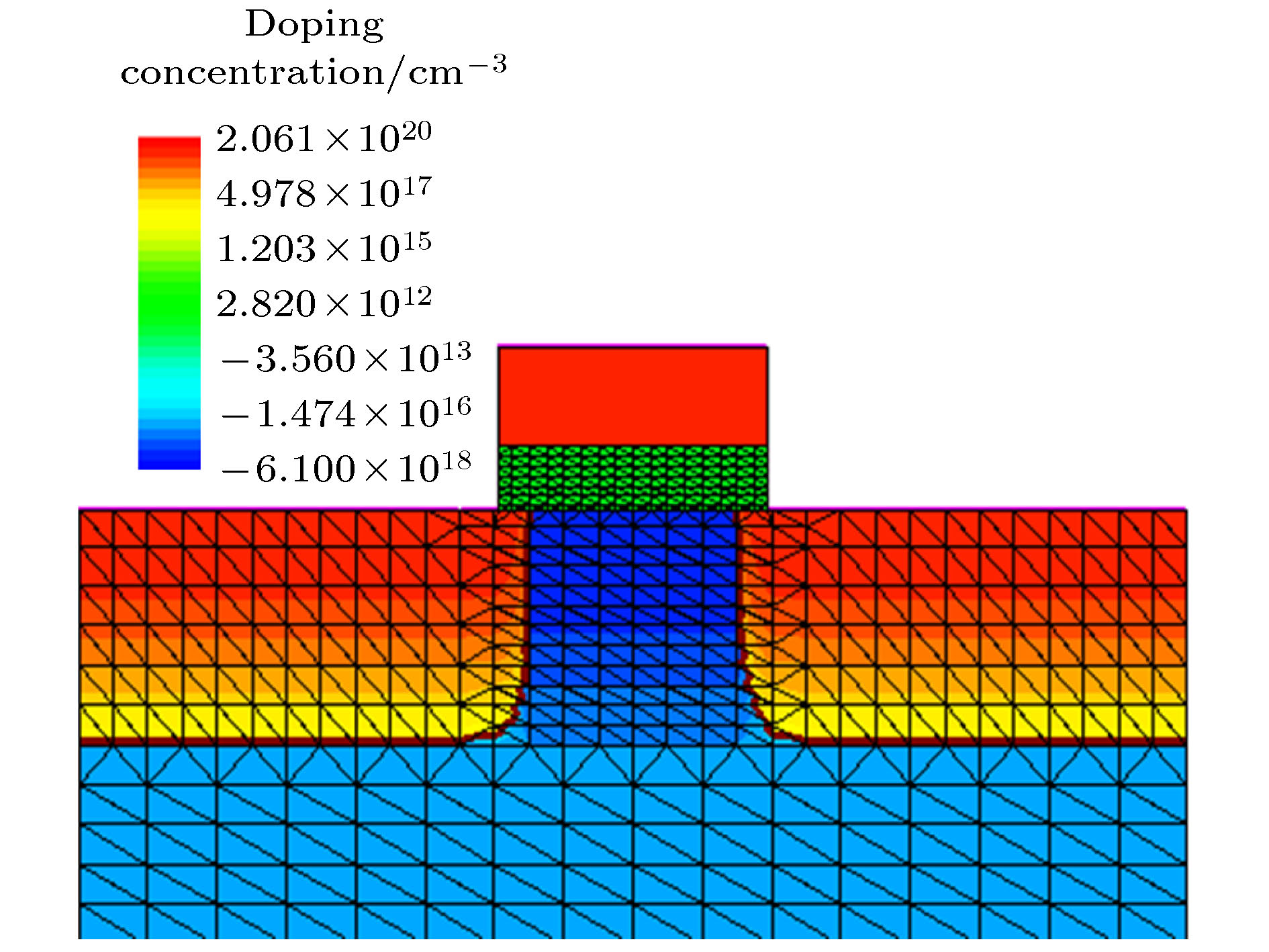 图 1 HfO2基FeFET器件物理模型
Figure1. Device physical models of HfO2-based FeFET.
| 参数 | 数值 |
| 多晶硅厚度/nm | 20 |
| 栅氧层厚度/nm | 1 |
| 铁电层厚度/nm | 10 |
| 沟道长度/nm | 45 |
| N型衬底浓度/cm–3 | 1 × 10¹⁶ |
| N阱浓度/cm–3 | 5 × 10¹⁶ |
| 源/漏浓度/cm–3 | 2 × 10²⁰ |
| 阈值电压掺杂浓度/cm–3 | 5 × 10¹⁷ |
| 饱和极化值Ps/μC·cm–2 | 28 |
| 剩余极化值Pr/μC·cm–2 | 23 |
| 矫顽场强度Ec/MV·cm–1 | 1 |
| 介电常数Eps | 22 |
表1HfO2基FeFET工艺参数
Table1.Process parameters of HfO2-FeFET.
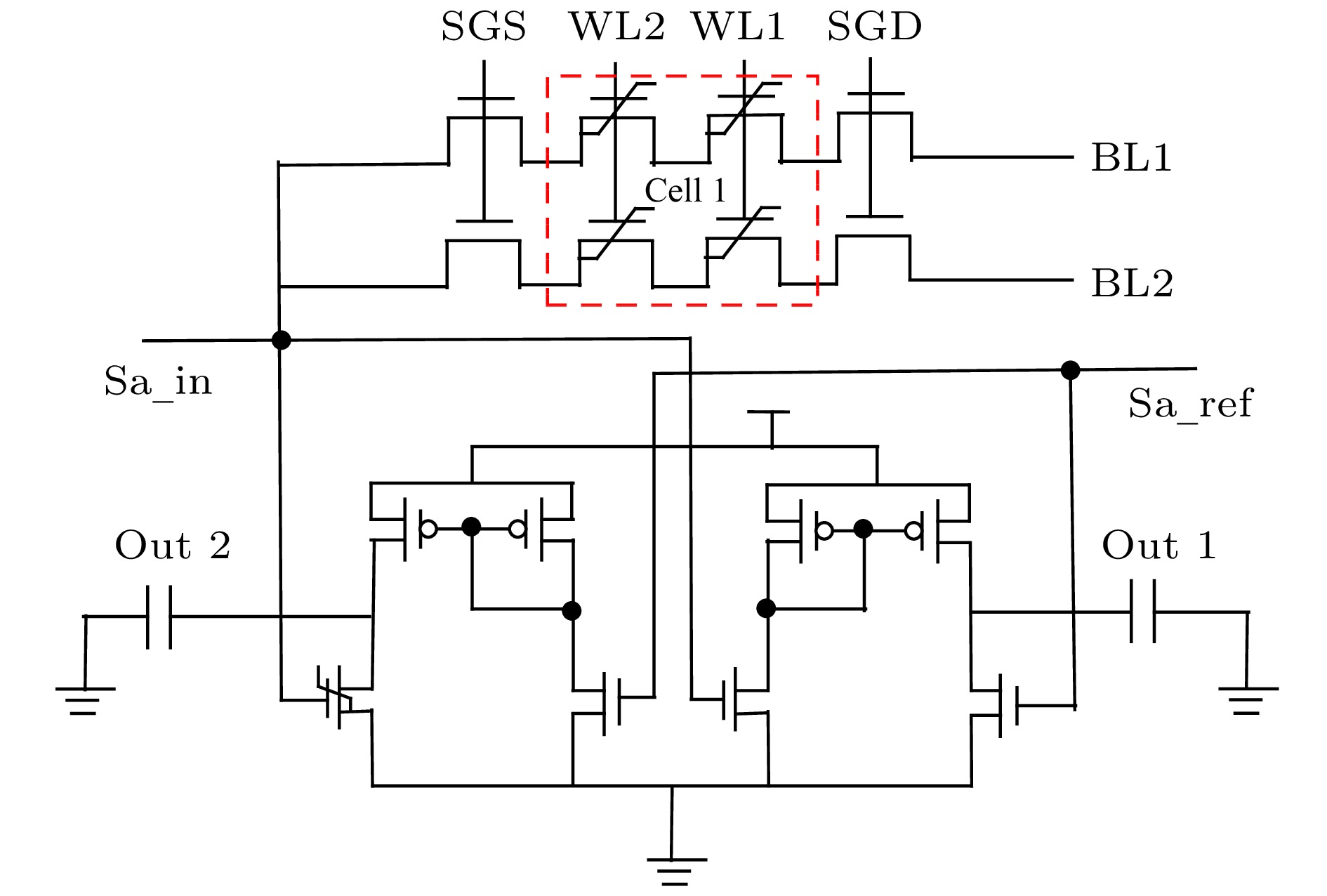 图 2 2 × 2铁电存储阵列的读写电路
Figure2. Read and write circuit of 2 × 2 ferroelectric memory array.
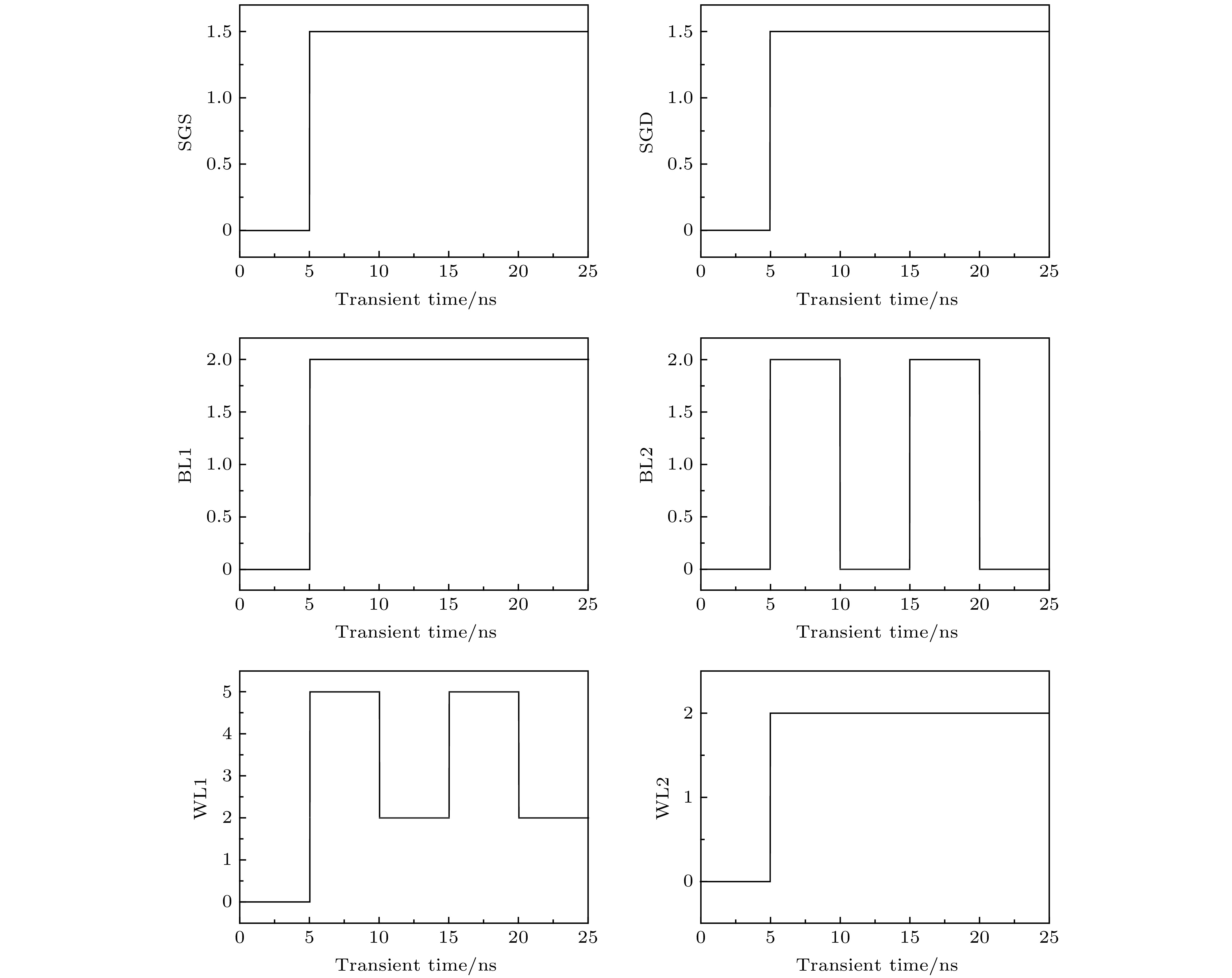 图 3 2 × 2铁电存储阵列控制仿真时序
Figure3. Control simulation timing of 2 × 2 ferroelectric memory array.
对于深亚微米级器件, 使用流体动力学模型去描述器件的载流子输运过程, 流体动力学模型有如下几个基本方程:
泊松方程


FeFET器件中铁电层和沟道是高掺杂区域, 在数值器件模拟中为了更贴合实际器件考虑了掺杂、电场以及载流子之间的散射和碰撞电离模型对迁移率的影响, 主要包括掺杂SRH复合模型、Auger复合模型和高浓度掺杂下的禁带变窄模型. 通过引入量子势(载流子浓度和浓度梯度的函数)来考虑量子效应, 在传输方程中还采用了密度梯度模型、泊松方程和载流子连续方程解算量子势方程. 影响晶体管物理模型电学特性的详见半导体器件仿真工具[26].
铁电性能模型能描述仿真模拟铁电电容的瞬态电学特性和非饱和状态下极化特性, 是根据Miller和Mcwhorter[28]提出的铁电模型进行了优化, 引入了铁电电容率模型, 通过搭建等效电路对铁电极化特征进行了全面准确的描述, 同时包括饱和极化模型和非饱和极化模型. 优化模型的具体表达式如下:
附加电场的瞬态变化,
采用了Gaussian分布建立单粒子辐射模型, 设置了轰击高能粒子的初始入射半径为0.05 μm, 入射深度为1 μm, 其他参数由TCAD默认设置. 详细求解高能粒子引起的电子空穴对产生率G的基本方程式如下:


对器件混合电路进行辐照模拟时, 首先通过(1)—(5)式和(9)式计算器件混合电路的电学特性求得稳态解, 然后结合单粒子辐射模型公式(10)计算出瞬态解.
3.1.HfO2基FeFET电路的读写
当栅极电压为负电压, 铁电极化从上指向下为负方向, 在沟道处有大量的累积电荷, 在漏源之间加小电压读出数据“0”; 当栅极电压为正电压, 铁电极化从下指向上为正方向, 沟道处出现了反型层, 在漏源之间加一个小电压读出数据“1”, HfO2基FeFET写入“1”和“0”状态时器件内部的电荷密度分布如图4所示. 输入2 × 2铁电存储阵列读写电路的控制时序如图3所示, 得到了HfO2基FeFET读写电路的灵敏放大器输出信号变化、铁电存储单元cell 1输出信号变化和铁电存储单元cell 1极化强度变化, 如图5所示. 通过输出电压的大小来定义存储状态“1”和“0”, 经过灵敏放大器进行数据读出. 当输入正栅压时, 铁电极化为正, 输出高电压为存储数据“1”; 当输入负栅压时铁电极化为负, 输出低电压为存储数据“0”.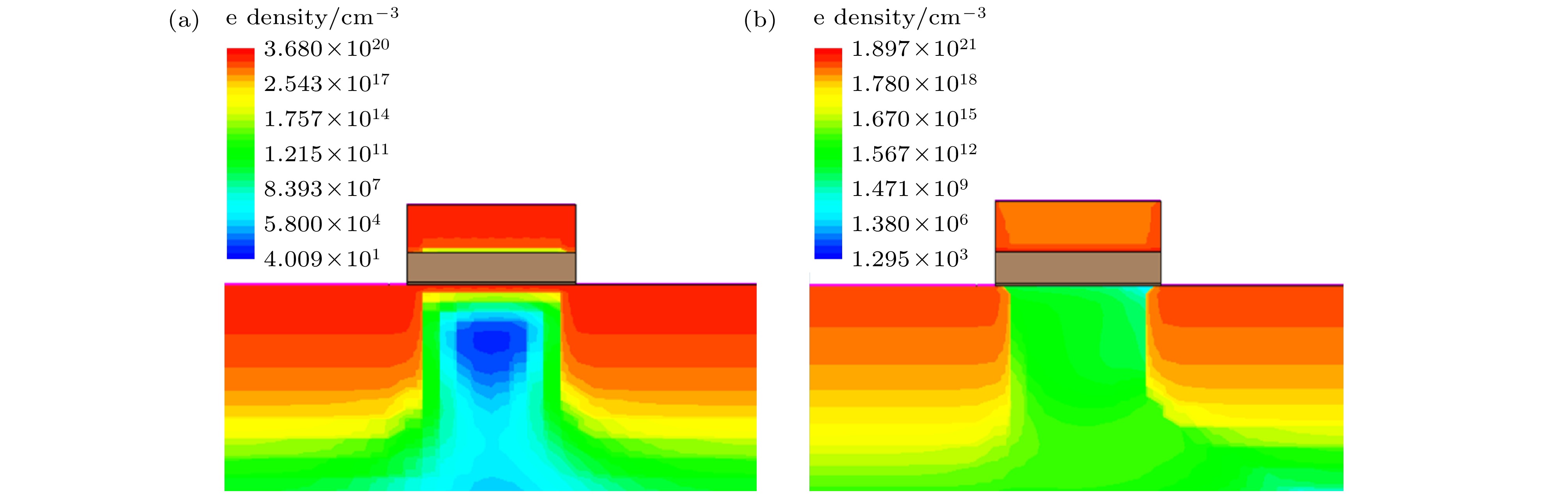 图 4 HfO2基FeFET写入时器件内部的电荷密度分布 (a)写入“1”器件内部电荷分布; (b)写入“0”时器件内部电荷分布
Figure4. Charge density distribution inside the device when HfO2-based FeFET is written: (a) The internal charge distribution of the device is written with “1”; (b) the internal charge distribution of the device is written with “0”.
 图 5 铁电存储阵列的读写信号 (a)灵敏放大器输出信号变化; (b) cell 1输出信号变化; (c) cell 1极化强度变化
Figure5. Reading and writing of ferroelectric memory arrays: (a) Changes in the output signal of the sense amplifier; (b) changes in the output signal of cell 1; (c) changes in the polarization of cell 1.
2
3.2.单粒子入射铁电存储管漏极对存储信息的影响
铁电存储单元作为FeFET读写电路的主要敏感节点之一, 其对单粒子瞬态效应的敏感度会直接影响数据的擦写, 因此非常有必要研究高能粒子入射其漏极的瞬态效应.图6为单粒子入射读写“0”的铁电存储单元cell 1时, 漏极的各节点瞬态效应变化. 图6(a)为高能粒子入射铁电存储单元cell 1漏极产生的漏极电流脉冲变化, 漏极电流脉冲随着高能粒子的LET值增加而变大. 如图6(b)所示, 在高能粒子入射存储管漏极后, 在cell 1内部产生了大量电子空穴对, 同时部分电子或空穴被漏极收集导致器件被迫导通, 电流方向变为负, 因此铁电存储单元cell 1输出电压从0 V变为负电压. 如图6(c)所示, 电子空穴对的产生增强了铁电存储单元cell 1栅极和基底的电场强度, 使得极化强度增大. 从图6(d)可以看出, 在读写“0”状态时, 高能粒子进入cell 1内部产生的微小收集电流经灵敏放大器放大后, 仅略微增大了输出电压, 数据能正确读出.
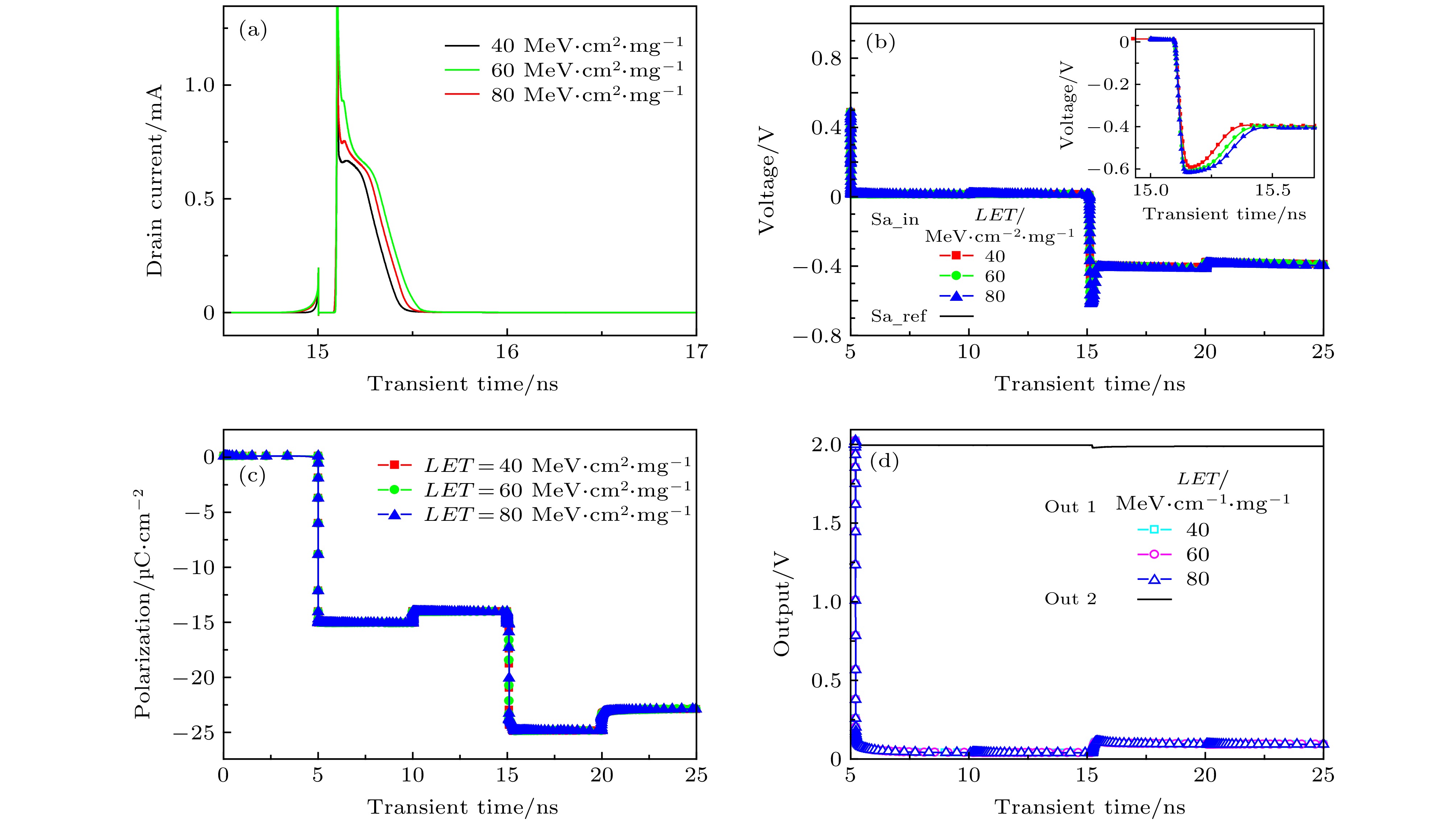 图 6 单粒子入射读写“0”铁电存储单元cell 1漏极的瞬态效应 (a) cell 1漏极电流脉冲变化; (b) cell 1输出信号变化; (c) cell 1极化强度变化; (d)灵敏放大器输出信号变化
Figure6. Transient effects of single-particle incident read and write “0” ferroelectric storage tube drain: (a) Change of drain current pulse; (b) change of cell 1 output signal; (c) change of cell 1 polarization intensity; (d) change of sense amplifier output signal.
从图7(a)铁电存储单元cell 1输出信号变化可以看出, 在高能粒子入射铁电存储单元cell 1漏极后, 铁电存储单元cell 1输出电压随着入射粒子的LET值增大而增大. 虽然在器件内部产生了大量电子空穴对, 但是此时cell 1处于开启状态, 电子空穴对能及时导出, 内部电场强度只是稍稍增大, 使得极化强度的变化没有图6(c)明显. 随着高能粒子LET值增大, 图7(b)中铁电存储单元cell 1输出瞬态电压峰值随着增大, 在高能粒子的LET值为30 MeV·cm2/mg时, 铁电存储单元cell 1输出电压的峰值接近于0 V, 在5 ns之后能恢复初始状态, 经过灵敏放大器放大后得到图7(c)灵敏放大器输出信号变化, 但是输出电压出现波动的时间只有0.5 ns, 从而数据能正常读出.
 图 7 单粒子入射读写“1”铁电存储单元cell 1漏极的瞬态效应 (a) cell 1极化强度变化; (b) cell 1输出信号变化; (c)灵敏放大器输出信号变化
Figure7. Transient effects of single-particle incident read and write “1” ferroelectric storage tube drain: (a) Change of cell 1 polarization intensity; (b) change of cell 1 output signal; (c) change of sense amplifier output signal.
为了更全面地分析单粒子入射铁电存储单元cell 1对存储信息的影响, 表2列出了不同LET值下输出端Out 1和Out 2之间的电位差变化. 尽管Sa_in和Sa_ref之间的电位差随着LET值的增加在不断减小, 但模拟中所采用的是理想型灵敏放大器能正确放大Sa_in和Sa_ref之间微小的电位差, 因此图7(c)中能够正确放大读出数据. 但是实际工作中没有理想型灵敏放大器, 灵敏放大器存在一个能够正确放大的最小输入电压差. 高能粒子入射铁电存储单元cell 1的漏极后, 在某个LET值下Sa_in和Sa_ref之间的电位差可能会小于灵敏放大器的最小分辨电压差, 导致数据信号不能正确放大读出以及回写, 引发单粒子翻转效应.
| LET值/MeV·cm2·mg–1 | |||||||
| 0 | 10 | 20 | 30 | 120 | 150 | 180 | |
| 电压差/V | 1.9 | 1.85 | 1.7 | 1.2 | 1 | 0.95 | 0.9 |
表2输出端Out 1和Out 2之间的电位差变化
Table2.Voltage difference change between Out 1 and Out 2.
2
3.3.单粒子入射放大器节点对存储信息的影响
灵敏放大器的作用是正确放大无法正常分辨的微弱信号, 转换为满足数据分辨功能要求的大输出信号, 因此放大器的灵敏节点对单粒子效应的敏感度是直接影响数据能不能正确放大读出的关键.图8为单粒子入射读写“0”时灵敏放大器输入管后铁电存储单元cell 1极化强度变化和灵敏放大器输出信号变化. 从图8(a)可知高能粒子入射读写“0”的灵敏放大器的输入管时, 对铁电存储单元cell 1极化强度几乎没有影响, 即数据可以正确读写. 图8(b)中高能粒子轰击灵敏放大器输入管产生了一个漏极脉冲电流, 灵敏放大器开始工作而放大输出电压, 灵敏放大器输出电压产生了很大的波动, 但是仅在0.4 ns后就恢复了初始状态, 因此数据能正常读出. 图9为读写“1”时, 单粒子入射灵敏放大器输入管后铁电存储单元cell 1极化强度变化和灵敏放大器输出信号变化. 从图9(a)可知铁电存储单元cell 1极化强度几乎没有影响, 存储单元能正确读写. 高能粒子轰击灵敏放大器输入管产生的漏极脉冲电流极小, 对读“1”时处于开启状态的灵敏放大器工作电流几乎没有影响, 输出信号数据能正常读出, 如图9(b)所示.
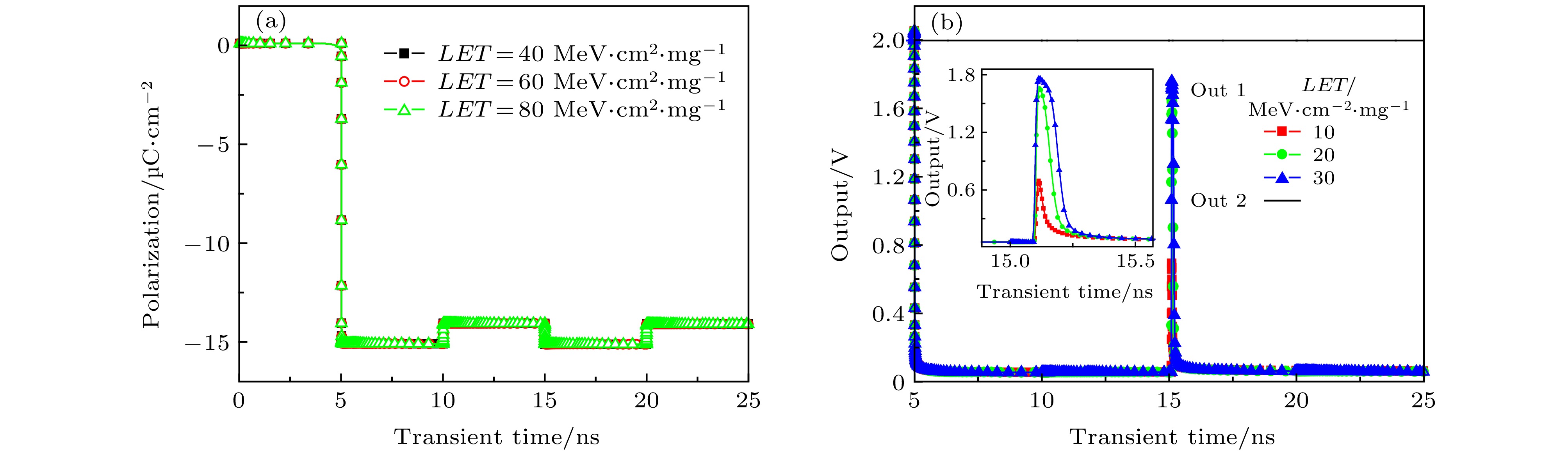 图 8 读写“0”时, 单粒子入射灵敏放大器输入管的瞬态效应 (a)铁电存储单元cell 1极化强度变化; (b)灵敏放大器输出信号变化
Figure8. Transient effects of a single-particle incident sensible amplifier input tube when reading and writing “0”: (a) Change of ferroelectric cell 1 polarization intensity; (b) change of sense amplifier output signal.
 图 9 读写“1”时, 单粒子入射灵敏放大器输入管的瞬态效应 (a)铁电存储管极化强度变化; (b)灵敏放大器输出信号变化
Figure9. Transient effects of a single-particle incident sensible amplifier input tube when reading and writing “1”: (a) Change of ferroelectric transistor polarization intensity; (b) change of sense amplifier output signal.
2
3.4.不同剩余极化和矫顽场强度对存储信息的影响
生长工艺、掺杂水平、厚度等原因致使HZO铁电薄膜具有不同的铁电性能. 因此, 分析HZO铁电薄膜有不同的剩余极化和矫顽场对研究结果的影响, 将使该模拟工作更具有实际应用价值. 铁电薄膜的存储能力决定了存储单元的存储性能. 图10(a)为不同剩余极化和矫顽场强度的HZO铁电薄膜下的铁电存储单元cell 1极化强度. 高能粒子在7 ns时进入cell 1漏极后, 管内电荷增加使得cell 1极化强度增高. 从图10(b)可知, 铁电薄膜的剩余极化强度越大, 铁电存储单元抗单粒子的能力越强, 在辐射环境下工作更加稳定. 图 10 单粒子作用于不同剩余极化和矫顽场的HZO铁电薄膜下的铁电存储单元cell 1的信号变化 (a) 铁电存储单元的极化强度变化; (b)灵敏放大器输出信号变化
Figure10. Signal change of ferroelectric memory cell cell 1 under single-particle HZO ferroelectric thin film with different remanent polarization and coercive field: (a) Change of ferroelectric transistor polarization intensity; (b) change of sense amplifier output signal.
2
3.5.多束高能粒子对存储信息的影响
两束LET值均为60 MeV·cm2/mg的高能粒子先后进入写“1”铁电存储单元cell 1后各节点的信号变化见图11, 时间间隔为0.5 ns. 在图11(a)中的脉冲电流有两个峰值, 时间间隔为0.5 ns. 在图11(b)和图12(a)中, 由于内部大量的电子空穴对使得极化强度增加, 其中图12(a)由于处于关态, 极化强度明显增大. 从图7(c)可知单个单粒子入射cell 1漏极后, 输出数据信号能迅速回复初始位置. 但是, 在图11(c)可以看到输出信号不能回复的初始状态, 且出现了双峰值, 最后两端输出的电压差减小, 影响数据正常的读出. 图12为两束LET值为60 MeV·cm2/mg高能粒子在时间间隔为0.5 ns先后进入写“1”状态的铁电存储单元cell 1后各节点的信号变化. 由图6(d)和图12(b)可以看出, 一束和两束高能粒子作用存储单元漏极都没有致使输出信号发生明显的波动, 说明处于关态的存储单元有很好的抗单粒子的能力.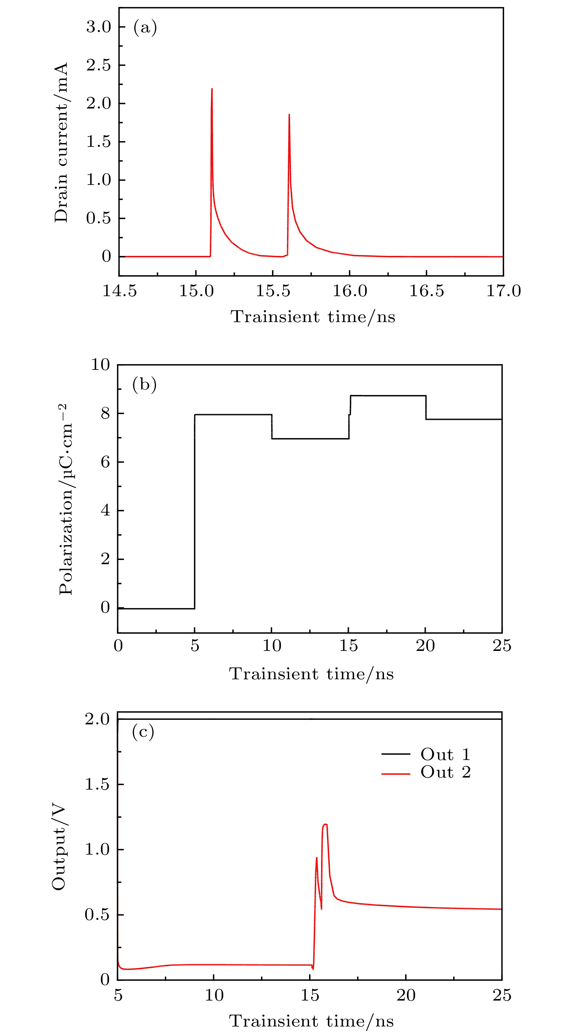 图 11 两束单粒子入射读写“1”铁电存储单元cell 1漏极的瞬态效应 (a) cell 1漏极电流脉冲变化; (b) cell 1极化强度变化; (c)灵敏放大器输出信号变化
Figure11. Transient effects of two single-particle incident read and write “1” ferroelectric storage tube drain: (a) Change of drain current pulse; (b) change of cell 1 polarization intensity; (c) change of sense amplifier output signal.
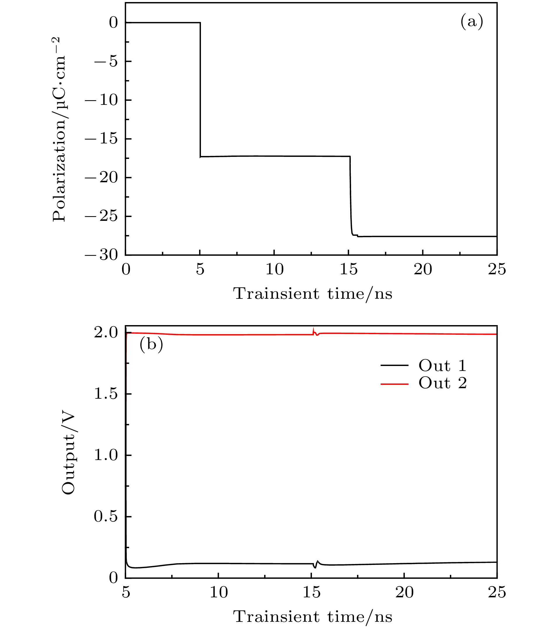 图 12 两束单粒子入射读写“0”铁电存储单元cell 1漏极的瞬态效应 (a) cell 1极化强度变化; (b) 灵敏放大器输出信号变化
Figure12. Transient effects of two single-particle incident read and write “0” ferroelectric storage tube drain: (a) Change of cell 1 polarization intensity; (b) change of sense amplifier output signal.
