Abstract:With the development of the integrated circuit manufacturing process, the device dimensions have been on a nanoscale, while the device performance, such as the mobility and thermal noise, is significantly affected by the hot-carrier effect, which further affects the channel thermal noise of the device. However, the thermal noise model based on the existing electron temperature expression does not take into account the influence of the temperature gradient on the electron temperature when it deals with the influence of the hot carrier effect. As the size of the device decreases, the thermal noise model based on the existing electron temperature expression underestimates the influence of the hot carrier effect and the channel thermal noise cannot be accurately predicted with this expression.In this paper, the expression of the channel transverse electric field is derived based on the channel potential equation and the boundary condition of the channel electric field. By combining the distribution of the temperature gradient and the expression of the transverse electric field, the energy balance equation is solved with considering the influence of the temperature gradient, and then the electron temperature expression is obtained. The electron temperature expression shows the distribution of the electron temperature along the channel. By utilizing the derived electron temperature expression and combining with the drain current expression, a channel thermal noise model is established. The hot carrier effect is taken into account in the thermal noise model by utilizing the proposed electron temperature expression. Meanwhile in calculating the thermal noise, the influence of the electron temperature on mobility degradation and the temperature gradient on thermal noise are also involved.The results show that the temperature gradient has a significant influence on the electron temperature with the reduction of the device size, which further increases the influence of the hot carrier effect, resulting in the increase of the thermal noise caused by the hot carrier effect exceeding the decrease of the thermal noise caused by the mobility degradation, thus leading the thermal noise to increase. The influence of the hot carrier effect on the channel thermal noise also increases significantly with the bias increasing. The channel thermal noise model proposed in this paper can be applied to analyzing the noise performance and modeling the nano-sized MOSFET devices. Keywords:electron temperature/ mobility degradation/ hot carrier effect/ temperature gradient/ channel thermal noise
图2为计算热噪声时的晶体管结构图[9]. 在NMOS器件的电子沟道区(沟道线性区)中, 设位于y = y1处的噪声电压源为Δv, 该电压源可看作是一个忽略长度的小虚拟直流电压源. 该电压源在带宽为Δf下的均方值, 如(16)式所示: 图 2 沟道坐标y = y1处有一虚拟直流源的晶体管结构图 Figure2. Schematic of the transistor with a fictitious dc source placed at point y = y1 in the channel.
$\overline {{{(\Delta v)}^2}} = 4{k_{\rm{B}}}{T_{\rm{e}}}\Delta R \cdot \Delta f,$
图 3 不同栅源偏置下的沟道热噪声与仅考虑沟道长度调制效应模型的对比(a); 以及与采用现有温度模型的对比(b) Figure3. The channel thermal noise at different gate-source bias: (a) Comparison with the model only considering the channel length modulation effect; (b) comparison with the model using the existing temperature model.
 图 1 NMOS器件的结构图


 图 2 沟道坐标y = y1处有一虚拟直流源的晶体管结构图
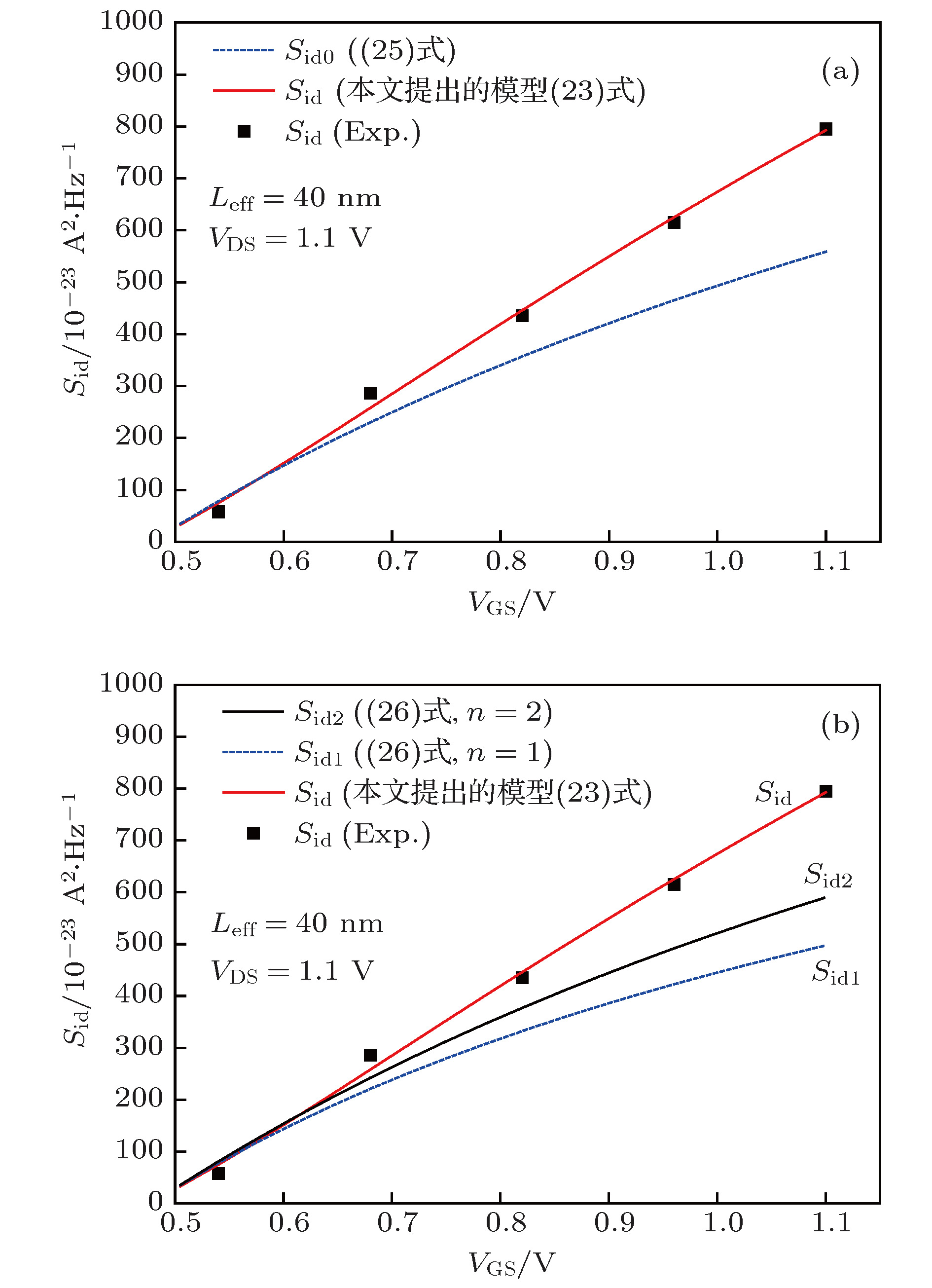 图 3 不同栅源偏置下的沟道热噪声与仅考虑沟道长度调制效应模型的对比(a); 以及与采用现有温度模型的对比(b)
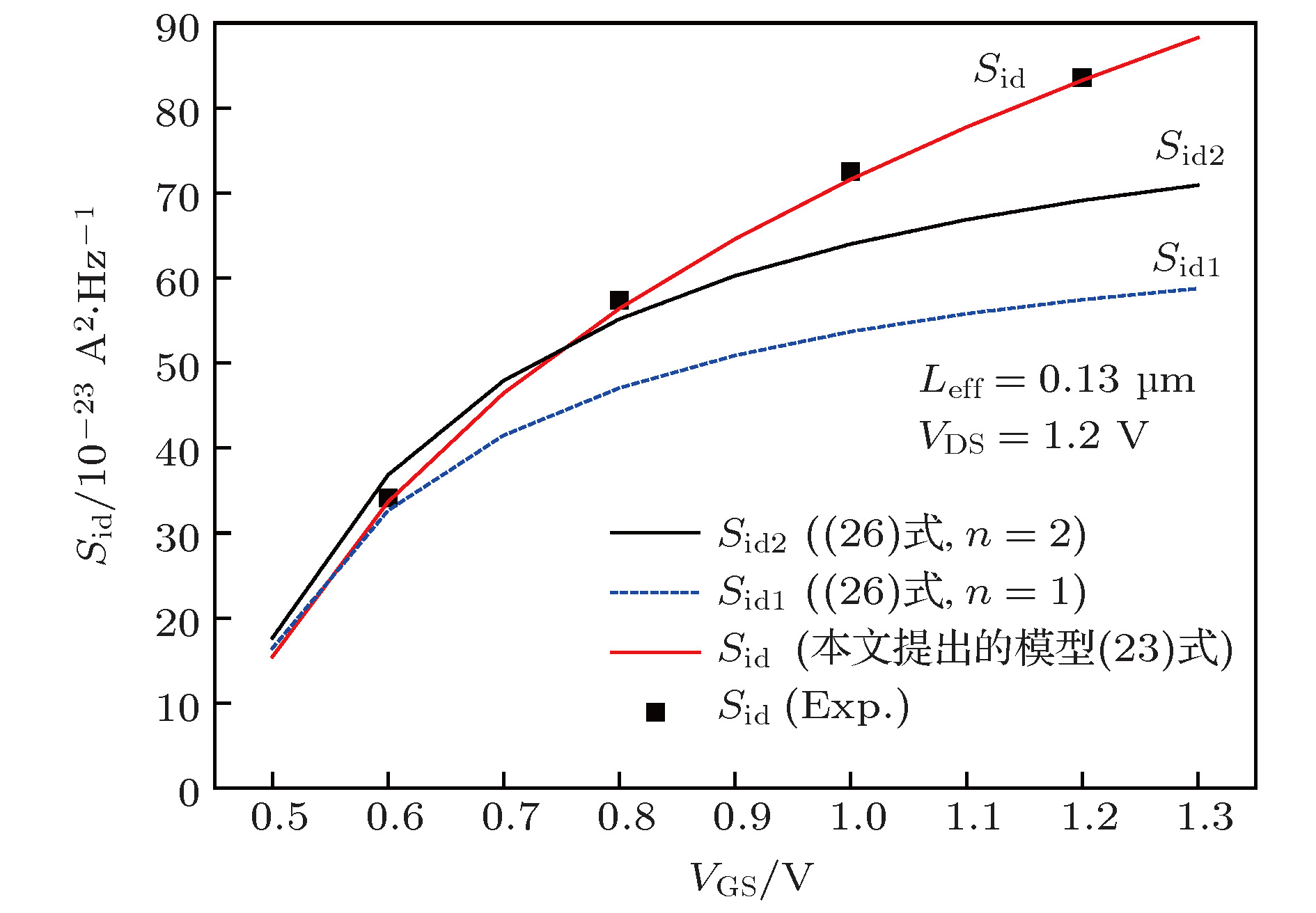 图 4 不同栅源偏置下的沟道热噪声(Leff = 0.13 μm)