1.School of Mechanics and Photoelectric Physics, Anhui University of Science and Technology, Huainan 232001, China 2.National Key Laboratory of Solid Microstructure Physics, Nanjing University, Nanjing 210093, China
Fund Project:Project supported by the National Laboratory of Solid State Microstructures, China (Grant No. M31041), the National Natural Science Foundation of China (Grant No. 11847002), and the Natural Science Foundation of Anhui Province, China (Grant No. 1908085QA21).
Received Date:02 March 2019
Accepted Date:18 April 2019
Available Online:01 August 2019
Published Online:05 August 2019
Abstract:Surface plasmons include surface plasmon polaritons and localized surface plasmons, which are electromagnetic wave confined at the interface of the metal and dielectric. Spoof surface plasmonic structure has many special optical properties, which is of great significance for designing new-generation optical elements. In order to transfer the features of the surface plasmon polaritons and localized surface plasmons to microwave-terahertz region, Pendry et al. (Pendry J B, Martin-Moreno L, Garcia-Vidal F J 2004 Science305 847) have proposed the spoof surface plasmon polaritons based on a metal structure with grooved stripes. In this paper, a hollow textured perfect electric conductor cylinder with periodic cut-through slits structure is designed to suppress the light scattering of the object in any direction and achieve the effect of omnidirectional cloaking while the transverse magnetic polarization wave propagates along the x direction. And the locations of the electrical and magnetic modes can be freely modulated by tailoring the structural geometric construction. In order to find the physical mechanism behind the abnormal phenomenon, through theoretical analysis and numerical simulation, we find that the strong scattering suppression of this spoof surface plasmonic polariton structure is caused by the interference between the background wave and Mie scattering of the structural unit, and it can be equivalent to a ring metamaterial due to the special structural design, in order to achieve the omnidirectional cloaking. It implies that we can hide objects in metal strips due to the fact that the metal in the microwave-to-terahertz region is equivalent to a perfect electrical conductor. This opens up a new way to analyzing the physical cloaking and optical response of spoof surface plasmonic polaritons structure. In addition, we also analyze the influence of the structure on the movement law of the scattering spectrum under different structural parameters. This enables us to have an in-depth understanding of the influence of structural parameters on the structural scattering spectrum. Our results can be applied to the microwave-to-terahertz region and a variety of advanced optic devices such as radars, cloaking coatings, sensors and detectors. Keywords:spoof surface plasmonic polaritons/ metamaterial/ structural scattering/ omnidirectional cloaking
全文HTML
--> --> --> 1.引 言自然界中无论是有生命的野生动植物还是无生命的物质, 模仿和隐身都是永恒的主题. 近年来随着科技的不断进步, 隐身技术在战机和雷达等军事武器中扮演着越来越重要的角色. 其中主流的隐身原理是基于变换光学和散射相消等[1-8]. 然而随着电磁波技术的不断进步, 利用结构共振散射与背景波干涉从而实现隐身的方法被提出, 也吸引了许多研究者的注意. 这种隐身原理主要是通过调节结构共振散射波与背景波峰的位置使得两者干涉相消, 从而使得结构的散射截面趋近于零, 实现隐身的效果. 变换光学的发展为利用麦克斯韦方程的不变性来变换空间和光的传播提供了新的工具. 基于2006年Pendry教授提出的变换光学理论[9], 人们开始可以设计人工材料从而实现对于电磁波的调控, 随后Smith教授等提出了第一个在微波频率段的二维柱状隐身结构[10], 2009年东南大学崔铁军教授课题组与Smith教授合作实现了微波频段的二维宽带隐身地毯[11]. 此外, Zharova等[12]还提出了一种基于结构自身利于共振散射波与背景波干涉实现隐身的方法同样引起了很大的关注, 通过调整结构的共振散射波与背景波的位置实现某一频率散射截面趋近于零从而达到隐身. 表面等离激元是在电磁波作用下和金属表面自由电子集体振荡产生的物理现象, 具有深度亚波长捕获和场增强等许多奇异的光学性质[13-15], 包括传播型等离激元和局域型等离激元. 由于在低频段情况下金属会被等效成为完美电导体, 所以表面等离激元性质不能在低频段实现. 为了在低频段利用等离激元实现许多奇异的光学现象, Pors等[16]提出了一种具有周期性金属条纹的结构, 可以将等离激元的许多奇异性质延伸到微波和太赫兹波区域. 这极大地推进了各类探究人工局域表面等离激元结构性质研究的进展, 如超薄人工局域表面等离激元金属盘结构和金属表面具有开放纹理的人工局域表面等离激元结构等[17-24]. 这种实心的人工局域表面等离激元结构在二维情况下磁模式会发生退化而只存在电模式. 为此, Wu等[25-27]提出了一种空心的人工局域表面等离激元结构, 可以实现在二维或三维结构中同时支持磁模式和电模式, 使得这种空心的人工局域表面等离激元结构可以实现类似于Mie共振的效应. 随后基于空心人工局域表面等离激元结构的定向电磁波散射和强Purcell效应等工作不断展开. 本文研究了一种可以同时支持电模式和磁模式的空心人工局域表面等离激元结构, 结果表明这种空心的人工局域表面等离激元结构具有类似于高折射率介电粒子中存在的Mie共振性质[28]. 通过调节这种人工局域表面等离激元的结构参数, 探究了人工局域表面等离激元结构的散射谱随着结构参数改变的规律. 此外, 使用了一种新的方法使得这种空心的人工局域表面等离激元结构实现了全方向隐身的效果. 该方法可以在不增加涂层的情况下大幅度地消除物体的散射截面. 这种隐身方法主要是基于结构的共振特性, 由于结构的电磁散射导致入射波与散射波之间会发生干涉相消[29]. 此研究结果适用于微波至太赫兹波区域, 为全向隐身提供了一种新的可行途径. 2.人工局域表面等离激元结构设计图1(a)所示为一种空心的人工局域表面等离激元结构. 空心硅盘结构的外半径和内半径大小分别为R和r, 插入完美电导体的裂缝深度h = R – r. 图1(b)为放大的结构基本单元, 裂缝的张角大小为a, 并且周期$ d = 2{\text{π}} R/N$(其中N为裂缝的总数). 向下的箭头代表着横磁(TM)极化波沿着y轴方向入射, 结构中蓝色部分选择了一种折射率n为4类似于硅的材料, 黄色部分代表着完美电导体, 整个结构被置于空气之中(区域I和II为空气). 我们发现区域II可以被等效为一个厚度h = R – r, εr = –∞, εθ = n2d/(d–a)和μz = (d–a)/d的超构材料(灰色部分). 图1(a)和图1(c)中的ρ和θ是极坐标. 在不失一般性的情况下, 除非本文另有说明, 否则选取的结构参数为N = 30, n = 4, a = 0.2d. 为了探测人工局域表面等离激元结构的共振模式, 使用一个沿y方向从上到下传播的TM极化平面波入射. 并使用基于有限元法的数值求解器计算了该人工局域表面等离激元结构的散射响应和场分布. 图 1 (a)人工局域等离激元的结构设计; (b)放大结构的基本构成模块; (c)等效的超构材料; (d)超构材料空间介电常数分布; (e)磁导率的空间分布 Figure1. (a) Structural design of spoof localized surface plasmonic; (b) the basic building blocks of the amplifier structure; (c) equivalent metamaterial; (d) spatial dielectric constant distribution of metamaterial; (e) the spatial distribution of permeability.
3.结构的电磁响应此结构的电磁响应可以通过计算散射截面得到精准的描述. 图2(a)给出了以频率为变量的人工局域表面等离激元共振结构的归一化散射截面谱, 散射截面被归一化至结构半径R. 在基于数值计算的基础上, 图2(a)给出了r = 0.1 m, R = 0.6 m时结构的总散射截面. 由图2(a)可以发现, 结构的散射谱中有许多共振峰, 为了进一步探究峰之间的区别, 将总散射谱分为两大区域, 蓝色区域的峰为低阶共振模式, 红色区域的峰为高阶共振模式. 散射谱中低阶与高阶模式中出现不对称的峰主要是由于空心人工局域表面等离激元结构的共振波与背景场相干产生的[30]. 为了进一步确认这些共振峰的模式, 给出了低阶区域中三个共振峰的近场分布Hz, 如图2(b)—图2(d), 可以发现从左到右分别对应着磁偶极模式、电偶极模式和电四极模式三个共振峰. 图 2 (a)计算的空心人工局域表面等离激元结构的散射谱, 其中浅蓝色区域代表低阶模式, 砖红色区域代表高阶模式; (b)?(d)低阶模式区域中三个共振峰的场分布, 分别对应于磁偶极模式、电偶极模式和电四极模式 Figure2. (a) Calculated scattering cross section spectrum for the textured perfect electric conductor hollow cylinder. The light blue and brick red area represent the lower and higher order mode, respectively. (b)?(d) The field distribution of three resonant peaks in the lower mode region correspond to magnetic dipole mode, electric dipole mode and electric quadrupole mode.
此外, 还研究了人工局域表面等离激元的结构参数对共振产生的影响, 分别研究了改变结构内半径r (图3(a))、外半径R (图3(b))、裂缝宽度和周期的比值a/d (图3(c))以及折射率n (图3(d))对等离激元结构共振峰移动产生的影响. 从图3(a)可以发现, 当裁剪结构内半径r从0.1 m增至0.2 m时, 这种带有金属波纹空心硅盘结构的共振峰会发生蓝移现象, 而当调节结构的外半径R从0.6 m增至0.7 m时, 结构的共振峰则会发生红移现象. 这是由于超构材料不仅对电场响应, 而且对磁场也响应, 所以当结构尺寸减小时电偶极模式和磁偶极模式都会发生蓝移. 如图3(c)所示, 当裂缝和周期的比值a/d从0.2改变至0.4时, 结构的散射谱会发生轻微的红移现象. 此外, 在图3(d)中还研究了电介质材料折射率对结构共振峰的影响, 发现随着折射率的变大结构的共振峰发生了红移. 这些研究结果表明, 通过裁剪结构的几何参数和调节相关材料, 可以灵活地调节人工局域表面等离激元结构共振峰的移动. 为了更加深入地了解空心的人工局域表面等离激元结构的共振响应, 应用电磁超构材料的概念给出了模拟空心人工局域表面等离激元结构散射截面的解析方程. 如图1(c)所示, 该结构可以看作一个TM极化平面波入射的厚度为R–r的空心超构材料圆柱, 所述超构材料的有效参数可以表示为[31] 图 3 计算的形变的具有完美电导体纹理的空心硅盘结构的散射谱 (a)改变内半径从0.1 m至0.2 m; (b)改变外半径从0.6 m至0.7 m; (c)裂缝a和周期d的比值从0.2至0.4; (d)电介质折射率大小从3改变至5 Figure3. Calculated scattering cross section of the textured perfect electric conductor hollow cylinder for changing: (a) Changing the inner radius from 0.1 m to 0.2 m; (b) outer radius from 0.6 m to 0.7 m; (c) the rations between the width of slit a and period d from a/d = 0.2 to a/d = 0.4; (d) the refractive index of the dielectric from n = 3 to n = 5.
4.人工局域表面等离激元的全向隐身著名的Mie散射理论是通过麦克斯韦方程组解析一个球的弹性散射电磁波所描述的[33-35]. 当一个球体的直径与入射波长相近, $ 2r\sqrt{\varepsilon }/\lambda \approx 1$时, Mie散射将会由介质球的共振驱动. 这就导致了背景源发出的电磁波和粒子非共振散射之间相互干扰, 当一个光谱较窄的Mie波段和一个较宽的辐射光谱发生相长或相消便可以预测会产生一个类似于Fano共振的现象[28,36]. 因此, 当我们的结构通过共振产生较窄共振峰的散射波和具有较宽共振峰的背景源波在通过两条不同的路径到达相同的最终状态时, 散射波和背景波会充当类似于Fano共振中的暗模式和亮模式[37-39], 此时空心的人工局域等离激元结构的散射波会和背景波发生干涉的效果, 当两者干涉相消时空心的人工局域表面等离激元结构的散射截面会发生大幅度降低以至于趋近于零而实现隐身的效果. 由于这种空心人工局域表面等离激元的特殊结构性质, 当TM极化平面波沿着结构四周的任意方向入射时本文结构都可以等效为一种环形的超构材料, 因此本文结构可以实现全方向隐身的效果. 为了验证这一现象, 计算了r = 0.3 m, R = 0.7 m, N = 30, n = 4和a = 0.8d结构参数下0.02—0.12 GHz之间的散射谱, 如图4(a)所示, 可以发现, 散射谱中出现了一个隐身点B, 此时结构的散射截面降低至零实现了隐身效果. 为了进一步对结果进行验证和对比, 挑选了散射谱上的三个点给出了它们的近场模式Hz分量, 如图4(b)—(d)所示, 红色圆圈内的黑点是结构, 图中内嵌的是放大红色圆圈内结构的近场分布图. 为了使结果具有较强的对比性, 我们选择分别在隐身位置两侧的点, A点和C点分别对应图4(c)和图4(d), 通过观察这两点位置下的近场模式图可以发现, 此时结构不可以实现隐身的效果, 而当结构处于图4(b)对应的B频率点时, 此时一束TM极化波入射到人工局域表面等离激元结构上时, 由于结构产生的人工局域表面等离激元散射波和背景源产生的波干涉相消从而实现了隐身效果. 图 4 (a)计算的r = 0.3, R = 0.7时具有完美电导体纹理的空心硅盘结构的散射谱; (b)在B位置时的场分布图, (c)和(d)分别对应着A点和C点的场分布图, 图中内嵌的图为红色圆圈内结构的放大 Figure4. (a) Calculated scattering cross section of the textured perfect electric conductor hollow cylinder at r = 0.3 m and R = 0.7 m; (b) field distribution at position B, (c) and (d) correspond to the field distribution of point A and point C respectively, the figure embedded in (b)?(d) shows the enlargement of the structure in the red circle.

 图 1 (a)人工局域等离激元的结构设计; (b)放大结构的基本构成模块; (c)等效的超构材料; (d)超构材料空间介电常数分布; (e)磁导率的空间分布
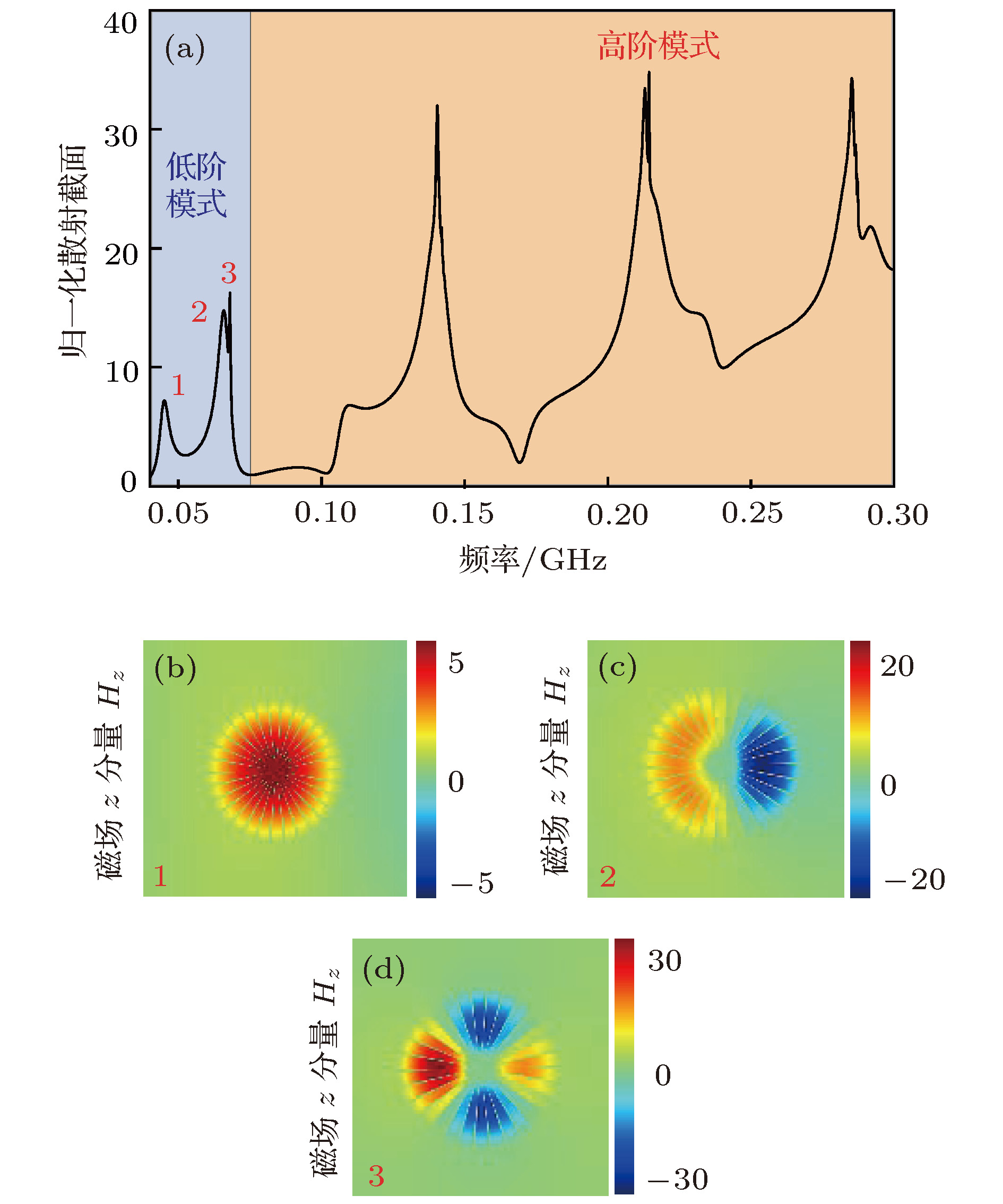 图 2 (a)计算的空心人工局域表面等离激元结构的散射谱, 其中浅蓝色区域代表低阶模式, 砖红色区域代表高阶模式; (b)?(d)低阶模式区域中三个共振峰的场分布, 分别对应于磁偶极模式、电偶极模式和电四极模式
 图 3 计算的形变的具有完美电导体纹理的空心硅盘结构的散射谱 (a)改变内半径从0.1 m至0.2 m; (b)改变外半径从0.6 m至0.7 m; (c)裂缝a和周期d的比值从0.2至0.4; (d)电介质折射率大小从3改变至5


 图 4 (a)计算的r = 0.3, R = 0.7时具有完美电导体纹理的空心硅盘结构的散射谱; (b)在B位置时的场分布图, (c)和(d)分别对应着A点和C点的场分布图, 图中内嵌的图为红色圆圈内结构的放大