全文HTML
--> --> -->阻变储存器结构一般为金属/存储介质/金属, 作为核心材料的存储介质一般为绝缘体或半导体, 常用的存储介质材料有金属氧化物[10-14]、有机物[15-18]和氧化物钙钛矿[19-22]等. 合成金属氧化物需要高温或溅射, 成本较高[23]; 有机物不稳定易分解[24]; 合成氧化物钙钛矿需要高温且氧化物钙钛矿薄膜表现为脆性, 不易于柔性器件的制备[25]. 近年来, 卤素钙钛矿因其制备工艺简单、光吸收系数大、带隙可调、载流子扩散距离长以及离子迁移速率快等优点而被广泛应用于光电器件领域[26-30], 如太阳能电池[31]、发光二极管[32]、场效应管[33]等. 其中铅基卤素钙钛矿因其特有的迟滞现象而被应用于阻变存储器[34-38]. 不足的是, 铅为重金属, 对人类健康及环境保护存在威胁, 限制了铅基卤素钙钛矿在数据存储领域的实际应用. 目前, 降低铅基卤素钙钛矿铅毒性成为了研究者们的研究热点. 其中, 非铅卤素钙钛矿因不含铅而被认为是最有前景的下一代新型阻变存储介质材料[39].
近年来, 国内外一些研究者对卤素钙钛矿阻变存储器进行了综述, Choi等[40]对有机-无机杂化卤素钙钛矿阻变性能进行了综述, Kim等[41]、Xiao等[42]、Jeong 等[43]以及Li等[44]对有机-无机杂化卤素钙钛矿和无机卤素钙钛矿阻变性能进行了综述. 针对非铅卤素钙钛矿及其阻变性能的综述鲜有报道. 因此, 本文对非铅钙卤素钛矿材料、阻变性能和阻变机理进行综述, 并指出非铅钙钛矿阻变存储器存在的关键问题, 为非铅卤素钙钛矿阻变性能的调控提供理论依据, 为开发新一代非铅高性能非易失性阻变存储器提供参考.
2.1.卤素钙钛矿简介
卤素钙钛矿的晶体结构见图1[45], 其化学分子式为ABX3, 其中A代表正一价的有机官能团或金属离子(如MA+(CH3NH3+), FA+(CH(NH2)2+), Cs+或Rb+), 位于原胞的8个顶点; B代表二价金属离子(如Pb2+或Sn2+), 位于四面体原胞中心; X代表卤素元素(Cl–, Br–或I–), 位于四面体的6个表面中心. 其中, 具有制备工艺简单、带隙可调、载流子扩散距离长以及离子迁移速率快的铅基卤素钙钛矿被广泛应用于太阳能电池、发光二极管、场效应管和阻变存储器等领域. 但铅属于重金属, 已被证实了会扰乱动物血液、肾脏、肝脏、睾丸、大脑以及神经系统的功能[46]. 因此, 针对含铅卤素钙钛矿结构中含重金属元素铅, 探索具有优异性能的非铅卤素钙钛矿成为了众多研究者新的探索领域. 目前, 对非铅卤素钙钛矿的研究主要有: 锡基卤素钙钛矿、锗基卤素钙钛矿、铋基卤素钙钛矿、锑基卤素钙钛矿和铜基卤素钙钛矿等. 图 1 卤素钙钛矿分子结构式ABX3 (A: 绿球, 代表正价金属离子或有机官能团. B: 蓝球, 代表金属阳离子. X: 红球, 代表卤素阴离子)[45]
Figure1. Crystal structure of trihalide perovskite with a chemical structure of ABX3, where A is the organic cation or metal cation (green), B is the metal cation (blue), and X is the halide anion (red)[45].
2
2.2.锡基卤素钙钛矿及其阻变性能
锡基卤素钙钛矿即采用二价锡(Sn2+)离子完全替代原卤素钙钛矿中的铅(Pb2+)离子, 构成ASnX3 (A = MA+, FA+或Cs+, X = Cl–, Br–或I–)卤素钙钛矿, 锡基卤素钙钛矿为直接带隙半导体, 其带隙低于1.4 eV, 具有激子结合能较低(仅18 meV)和超载流子迁移率的特点[47], 广泛应用于太阳能电池领域, 少量应用于阻变存储器. 目前报道具有阻变性能的锡基卤素钙钛矿主要有CsSnBr3和CsSnI3. 光滑致密的CsSnBr3钙钛矿薄膜以及Pt/CsSnBr3/Pt/PET柔性阻变存储器是由Wang等[48]采用气相沉积法获得, 该器件的开/关比为105, 但其耐受性在空气中测试仅为50 (如图2所示). 此外, Han等[49]采用氢碘酸对CsSnI3非铅卤素钙钛矿进行修饰, 制备了Ag或Au/PMMA/CsSnI3/Pt/Ti/SiO2/Si阻变存储器(如图3所示), 采用Ag电极所获得器件的操作电压极低, 低于0.15 V, 开/关比为104, 耐受性测试可达600次, 但器件的保持时间仅为7 × 10³ s, 且测试坏境必须为真空条件. 这主要是由于CsSnBr3和CsSnI3晶体结构中的二价Sn2+离子在空气中易被氧化成四价Sn4+离子, 导致CsSnBr3和CsSnI3结构不稳定, 阻态保持时间太短, 因此, 测试需在真空条件或保护气体(N2或Ar2)氛围进行, 限制了它的实际应用. 图 2 CsSnBr3非铅钙钛矿材料阻变性能 (a) Pt/CsSnBr3/Pt/PET阻变存储器结构示意图; (b)电流-电压(I-V )特性曲线; (c)耐受性[48]
Figure2. Resistive switching performance of CsSnBr3 lead-free halide perovskite: (a) Schematic of Pt/CsSnBr3/Pt/PET resistive switching device; (b) typical current-voltage (I-V ) curve; (c) endurance performance[48].
 图 3 CsSnI3非铅钙钛矿材料及其阻变性能 (a) CsSnI3晶体结构; (b)阻变存储器结构; (c)器件的截面SEM图; Ag/CsSnI3/Pt/Ti/SiO2/Si器件的(d) I-V特性曲线、(e)耐受性和(f)高低阻态保持特性; Au/CsSnI3/Pt/Ti/SiO2/Si器件的(g) I-V特性曲线、(h)耐受性和(i) 50个不同元器件高低阻态[49]
Figure3. Resistive switching performance of CsSnI3 lead-free perovskite: (a) CsSnI3 crystal structure; (b) schematic of the Ag or Au/PMMA/CsSnI3/Pt/SiO2/Si vertical stack structure; (c) cross-sectional SEM image of the device; (d) the typical I-V curves, (e) endurance performance, and (f) retention characteristics of low resistances state (LRS) and high resistance state (HRS) of the Ag/PMMA/CsSnI3/Pt devices; (g) the typical I-V curves, (h) endurance performance, and (i) HRS and LRS of 50 different cells of the Au/PMMA/CsSnI3/Pt devices[49].
2
2.3.锗基卤素钙钛矿及其阻变性能
锗基卤素钙钛矿即铅基卤素钙钛矿的Pb2+离子被二价的锗离子(Ge2+)完全替代, 构成AGeX3( 图 4 (a) CsGeI3, (b) MAGeI3和(c) FAGeI3的表面扫描电子显微镜(SEM)图谱[50]
Figure4. Scanning electron microscope (SEM) images of (a) CsGeI3, (b) MAGeI3, and (c) FAGeI3 films[50].
2
2.4.铋基卤素钙钛矿
元素周期表中, 铋(Bi)元素与Pb挨得很近, Bi具有与Pb类似的6s26p0电子结构, 因此, 铋基卤素钙钛矿具有光吸收能力强、载流子寿命长等特点. 不同于Pb2+离子, 铋离子常见的为正三价Bi3+离子, 因此, 采用Bi构建的铋基非铅卤素钙钛矿与铅基卤素钙钛矿晶体结构有所不同, 与铅基、锡基或锗基卤素钙钛矿相比, 铋基卤素钙钛矿在Bi


 图 5 铋基非铅卤素钙钛矿晶体结构 (a) Rb3Bi2I9[52]; (b) Cs3Bi2I9[52]; (c) CsBi3I10[53]
Figure5. Crystal structure of Bi-based perovskite: (a) Rb3Bi2I9[52]; (b) Cs3Bi2I9[52]; (c) CsBi3I10[53].
 图 6 铋基非铅卤素钙钛矿阻变存储器 (a) Au/A3Bi2I9/Pt/Ti/SiO2/Si器件结构示意图; (b) Rb3Bi2I9阻变存储器截面SEM图; (c) Cs3Bi2I9阻变存储器截面SEM图; Rb3Bi2I9阻变存储器的(d) I-V特性曲线、(e)耐受性和(f)保持特性; Cs3Bi2I9阻变存储器的(g) I-V特性曲线、(h)耐受性和(i)保持特性[52]
Figure6. The Bi-based perovskite resistance random access memory (ReRAM) devices: (a) Schematic of Au/A3Bi2I9/Pt/Ti/SiO2/Si based ReRAM devices; (b) the cross-section SEM image of Rb3Bi2I9 based ReRAM device; (c) the cross-section SEM image of Cs3Bi2I9 based ReRAM device; (d) the typical I-V curve, (e) endurance, and (f) retention of Rb3Bi2I9 based ReRAM; (g) the typical I-V curve, (h) endurance, and (i) retention of Cs3Bi2I9 based ReRAM[52].
 图 7 Al/CsBi3I10/ITO阻变存储器 (a)阻变存储器结构; (b)稳定性; (c)保持特性; (d)耐受性[54]
Figure7. Al/CsBi3I10/ITO ReRAM device[54]: (a) Schematic; (b) stability; (c) retention; (d) endurance.
 图 8 (a) Cs2AgBi2Br6的晶体结构; (b) Au/Cs2AgBi2Br6/ITO阻变存储器的截面SEM; (c)循环耐受性[55]
Figure8. (a) Crystal structure of Cs2AgBi2Br6; (b) the cross-section SEM image and (c) the cycle endurance characteristics of Au/Cs2AgBi2Br6/ITO ReRAM[55].
 图 9 Au/Cs2AgBi2Br6/ITO 器件在不同恶劣环境下的I-V特性曲线 (a)相对湿度(RH) 10%—80%; (b)温度范围为303—453 K; (c)酒精灯外焰加热10 s; (d)在60Co射线照射下曝露, 总剂量高达5 × 10⁵ rad(SI)[55]
Figure9. I-V characteristics of Au/Cs2AgBi2Br6/ITO device in different harsh environments: (a) 10%—80% relative humidity; (b) temperature range from 303 to 453 K; (c) burnt by luminous cone of alcohol lamp for 10 s; (d) exposed under 60Co γ-ray irradiation with a total dose as high as 5 × 10⁵ rad (SI)[55].
2
2.5.锑基卤素钙钛矿
锑(Sb)位于元素周期表中Pb的右上角, 其三价阳离子Sb3+具有与二价Pb2+离子相似的电子构型. 将锑化合物作为人类利什曼病的治疗剂研究已有报道, 证明了锑化合物的低毒性[56], 因此, 人们预计Sb也是铅的无毒替代品. 由于Sb具有高氧化态(+3), 锑基非铅卤素钙钛矿具有低维尺寸的晶体结构, 易形成二聚体结构或层状结构, 典型的化学结构为A3Sb2X9 ( 图 10 (a) Ag/PMMA/MA3Sb2Br9/ITO阻变存储器结构示意图; (b) MA3Sb2Br9晶体结构; (c) MA3Sb2Br9薄膜截面SEM图; MA3Sb2Br9基阻变存储器的(d) I-V特性曲线、(e)耐久性和(f)保持时间; (g)依赖于连续脉冲的长期增强(LTP)和长期抑制(LTD)现象; (h)突触前和突触后突峰(用于模拟突峰时间依赖性可塑性(STDP)); (i) STDP行为[58]
Figure10. (a) Schematic device structure of Ag/PMMA/MA3Sb2Br9/ITO ReRAM; (b) crystal structure of MA3Sb2Br9; (c) cross-sectional SEM image; (d) I-V characteristics, (e) endurance, and (f) retention time of MA3Sb2Br9 based memristors; (g) long-term potentiation (LTP) and long-term depression (LTD) depending on consecutive pulses; (h) presynaptic and postsynaptic spikes for emulating spike timing dependent plasticity (STDP); (i) STDP behavior of an MA3Sb2Br9 memristor[58].
2
2.6.铜基卤素钙钛矿
铜(Cu)是过渡金属, 作为酶的一部分在人体中必不可少, 可用于医学研究和临床实践. 例如用于癌细胞的放射治疗[59]. 在日常生活中可用作普通导体, 与具有3维结构的铅基卤素钙钛矿不同, 铜由于具有较小的离子半径, 且具有两种化合价, 能构建的结构有很多. 电子结构为3d9(

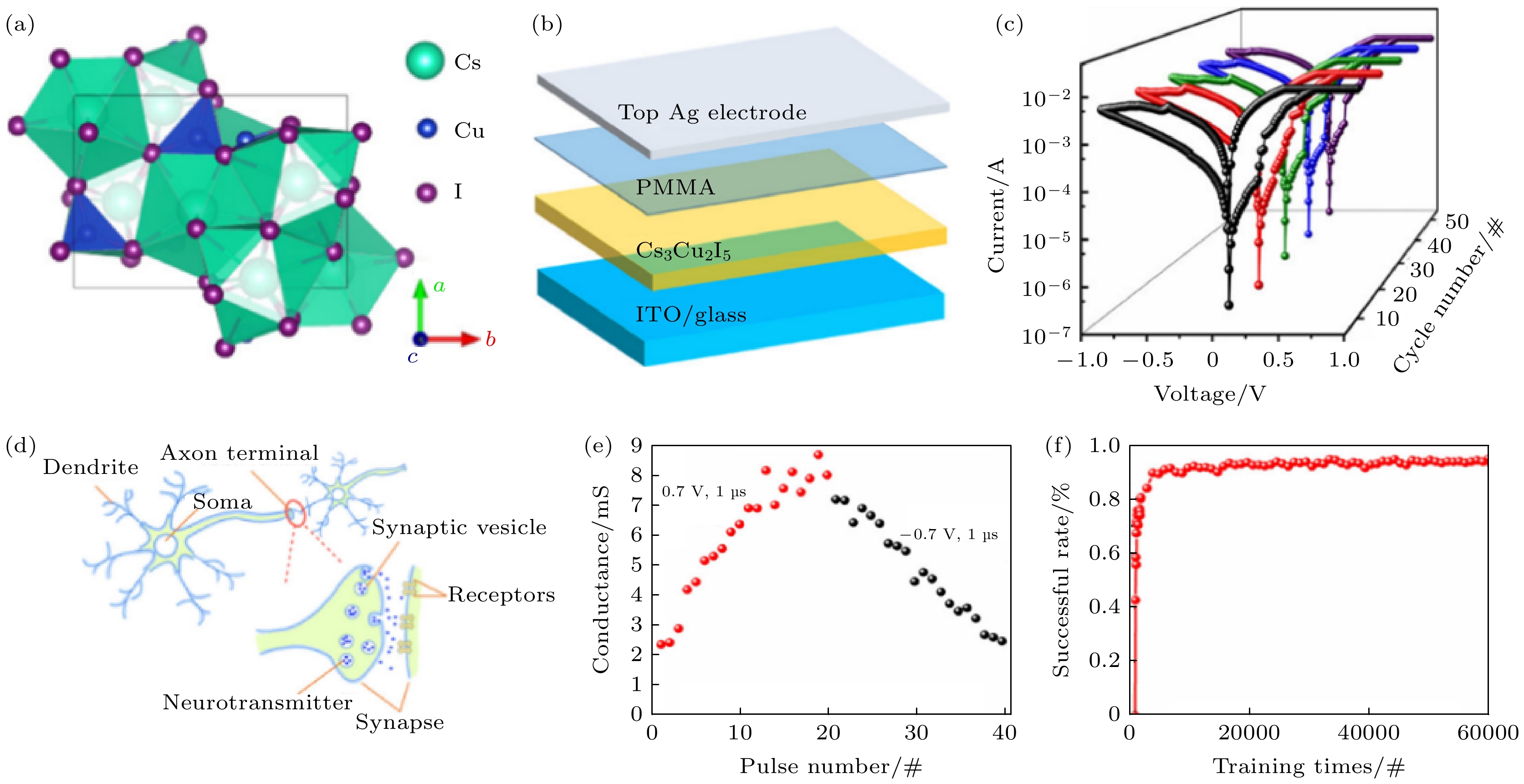 图 11 (a) Cs3Cu2I5非铅钙钛矿晶体结构; Cs3Cu2I5阻变存储器的(b)垂直结构示意图和(c)循环测试; (d)模拟神经突触示意图; (e)线性增强和线性抑制; (f)美国国家标准技术研究院数据库(MNIST)训练数据识别精度[65]
Figure11. (a) Cs3Cu2I5 crystal structure; (b) vertical stack structure schematic and (c) cycle tests of the Ag/PMMA/Cs3Cu2I5/ITO memristor; (d) schematic of synapses; (e) linear potentiation and depression; (f) successful recognition accuracy monitored while training the data set from Modified National Institute of Standards and Technology (MNIST)[65].
2
3.1.导电细丝模型
导电细丝模型可分为电化学金属模型(ECM)和价态改变模型(VCM), ECM模型如图12(a)所示. 常见的非铅卤素钙钛矿阻变存储器的结构为: 顶电极(活性金属)/非铅卤素钙钛矿/底电极(惰性电极), 向顶电极施加正向电压时, 活性金属电极将发生氧化还原反应, 在非铅卤素钙钛矿层形成导电细丝, 器件置于低阻态; 反之, 若施加反向电压, 导电细丝断裂, 器件被重置于高阻态, 在周期性电压的作用下, 器件实现了高阻态与低阻态的连续切换(图12(c)). 图 12 (a) ECM机理; (b) VCM机理; (c)导电细丝在存储介质层的形成和断裂示意图
Figure12. (a) ECM switching mechanism; (b) VCM switching mechanism; (c) the schematic illustration of filament formation and rupture in the switching layer.
VCM如图12(b)所示, 不同于ECM模型, 该器件以非铅卤素钙钛矿存储介质介于两惰性电极之间构成阻变存储器, 在电场作用下, 卤素钙钛矿内的缺陷态(如碘空位VOI或溴空位VOBr)产生迁移, 形成导电细丝, 变换电压极性, 导电细丝断裂. 例如, 将Cs3Bi2I9[52]置于惰性电极Au与Pt电极之间, 其阻变特性主要由碘空位VOI导电细丝的形成与断裂控制, 实现高阻态与低阻态的切换; 分别将CsSnBr3[48]或Cs2AgBiBr6[55]介于惰性电极Au及Pt电极之间, 在电场作用下, 其阻变特性主要由VOBr导电细丝的形成与断裂控制, 实现高阻态与低阻态的切换(图12(c)).
2
3.2.界面模型
在非铅卤素钙钛矿阻变存储器中, 存储介质材料与电极材料的接触方式有欧姆接触与肖特基接触, 欧姆接触即非铅卤素钙钛矿与电极材料的费米能级接近, 电流-电压呈线性关系, 而肖特基接触则是非铅卤素钙钛矿与电极材料的功函数相差很大, 导致界面处形成肖特基势垒. 在外加电场作用下, 肖特基势垒宽度会随电压极性发生改变, 可移动电子浓度随着势垒宽度改变而改变, 使得器件在高阻态与低阻态之间发生切换. Han等[49]所报道的Au/PMMA/CsSnI3/Pt/Ti/SiO2/Si卤素钙钛矿存储器中(图13), Au与PMMA/CsSnI3的界面处由于功函数相差较大, 形成肖特基接势垒, 在Au顶电极施加正向偏置电压时, 锡空位在顶电极与p型钙钛矿层的界面积累, 耗尽层宽度减小, 电子更容易隧穿通过肖特基势垒, 器件被置于低阻态; 当顶电极施加反向偏置电压时, 界面上的锡空位减少, 势垒宽度增加, 器件被置于高阻态. 图 13 (a) Au/PMMA/CsSnI3/Pt器件界面型机理示意图[49]; (b)电场作用下, p型钙钛矿层中锡空位的积累引起的耗尽宽度变化[49]; (c)界面型机理示意图
Figure13. (a) Schematic of the interface-type switching mechanism in the Au/PMMA/CsSnI3/Pt device[49]; (b) depletion width variation in the p-type perovskite layer according to the accumulation of Sn vacancies under an electric field[49]; (c) the schematic illustration of interface-type switching mechanism in the switching layer
| 器件结构 | 设置/重置电压/V | 开/关比 | 耐受性/次 | 保持特性/s |
| Pt/CsSnBr3/Pt/PET[48] | 0.2/–0.15 | 105 | 50 | 104 |
| Ag/PMMA/CsSnI3/Pt/Ti/SiO2/Si[49] | 0.15/–0.3 | 104 | 600 | 7 × 10³ |
| Au/Cs3Bi2I9/Pt/Ti/SiO2/Si[52] | –0.5/0.1 | 107 | 400 | 103 |
| Au/Rb3Bi2I9/Pt/Ti/SiO2/Si[52] | –0.5/0.09 | 107 | 100 | 103 |
| Al/CsBi3I10/ITO[54] | –1.7/0.9 | 103 | 100 | 104 |
| Au/Cs2AgBiBr6/ITO[55] | –3.4/2 | 102 | 103 | 105 |
| Au/Cs3Bi2I9/ITO[66] | –0.5/0.3 | 102 | 103 | 104 |
| Ag/PMMA/MA3Sb2Br9/ITO[58] | 2.5/–0.5 | 102 | 300 | 104 |
| Ag/PMMA/Cs3Cu2I5/ITO[65] | –1/0.75 | 102 | 100 | 104 |
表1基于非铅卤素钙钛矿的阻变存储器的阻变性能
Table1.Resistive switching performance of resistive switching memory parameters based on lead-free halide perovskites.
