Fund Project:Project supported by the National Natural Science Foundation of China (Grant Nos. 51602013, 12004021), the Young Elite Scientists Sponsorship Program by China Association for Science and Technology (CAST) (Grant No. 2018QNRC001), the International Collaboration 111 Project, China (Grant No. B16001), the Fundamental Research Funds for the Central Universities of China, and the Beijing Advanced Innovation Centre for Big Data and Brain Computing (BDBC)
Received Date:15 December 2020
Accepted Date:03 January 2021
Available Online:10 June 2021
Published Online:20 June 2021
Abstract:Recently, the discovery of intrinsic two-dimensional (2D) ferromagnetism has accelerated the application of spintronics in ultra-low power electronic device. Particularly, the Curie temperature of Fe3GeTe2 can be improved to room-temperature in several ways, such as interfacial exchange coupling and ionic liquid gating, which makes Fe3GeTe2 desirable for the practical application. In this work, we investigate the transport properties of Fe3GeTe2/graphene heterostructures with or without h-BN layers by utilizing the density functional theory combined with nonequilibrium Green’s function method. The results show that due to electronic orbital hybridization, the spin can be effectively injected into graphene with ± 0.1 V bias at the transparent contact interface of Fe3GeTe2/graphene. What is more, the efficient spin tunneling injection can be achieved in a wider bias range [–0.3 V, 0.3 V] by adding h-BN as a tunneling layer, where the spin filter effect that is induced by mismatched distribution of spin-dependent electronic states in the Brillouin zone, leads a spin polarizability to approach 100%. These results are helpful in the applications of 2D all-spin logic and the development of ultra-low power spintronic devices. Keywords:two-dimensional magnet/ spin injection/ spin filter effect/ first principles calculation
2.计算模型与理论方法本文采用经典的两端口器件模型来进行计算, 如图1所示, 包括由Fe3GeTe2构成的左电极, 石墨烯构成的右电极和Fe3GeTe2/氮化硼/石墨烯层状异质结构成的中心透射区. 其中, 以氮化硼的层数为0层或者3层来模拟实验上的透明接触和隧穿接触两种接触情况. 其中, Fe3GeTe2选取1 × 1晶胞(a = b = 3.991 ?), 而石墨烯和氮化硼选取$\sqrt{3} \times \sqrt{3}$超胞来使晶格与Fe3GeTe2匹配[22], 其晶格失配度分别为6.5%和7.8%. 本文基于VASP (Vienna ab initio simulation package)中的密度泛函分析方法对器件结构进行了优化[26], 截断能取值为400 eV, 布里渊区是由以Γ点为中心21 × 21 × 1的Monkhorst网格采样, 设定力的收敛准则为0.01 eV/A. 在此基础上本文利用Nanodcal软件包基于密度泛函理论结合非平衡态格林函数来进行输运计算[27-29]. 输运计算过程中, 基组函数通过双Zeta加极化(double-zeta plus polarization, DZP)轨道基集的线性组合(linear combination of atomic orbital, LCAO)来描述原子. 交互关联能采用考虑线性自旋极化的局域密度近似(local density approximation, LDA), 截止能取值为160 Ry. 在输运计算过程中, 左右电极的自洽计算采用100 × 9 × 100的k点网络抽样, 中心区采用1 × 9 × 100的k点网络抽样, 对应器件的输运方向沿着x和z轴, 如图1所示. 为了防止z轴上周期性重复带来的影响, 在器件z轴上加入了15 ?真空层. 在进行平衡态输运计算时, 通过对布里渊区的透射系数取平均得到对应能量下的透射系数: 图 1 Fe3GeTe2/氮化硼(3)/石墨烯器件的(a)侧视图和(b)俯视图, 其中器件的电极区域由虚线框标出; 在器件的中心透射区Fe3GeTe2和石墨烯之间有0层或者3层氮化硼, 这里所示的模型是具有3层氮化硼的器件结构 Figure1. (a) The side view and (b) top view of Fe3GeTe2/h-BN(3)/graphene devices. The electrode regions of the device are indicated by a dashed frame. The number of h-BN layers between graphene and Fe3GeTe2 in the center region is 0 or 3. The model shown here is the device structure with 3 layers h-BN.
3.计算结果与分析利用单层Fe3GeTe2向石墨烯注入自旋的结果如图2所示. 图2(a)和图2(b)分别是在没有氮化硼作隧穿层的器件中的I-V特性曲线和对应的自旋极化率. 从图2(a)可以看到自旋向上的电流明显高于自旋向下的电流, 这表明有很好的自旋注入效果. 实际上, 在低偏压 ± 0.1 V下, 石墨烯中的自旋极化率高达93.3% (图2(b)). 不过, 随着偏压的增大, 自旋向下电流也逐渐增大, 使得自旋极化率逐渐下降, 在 ± 0.3 V偏压下只有60%左右. 图 2 (a) 透明接触器件的I-V曲线; (b) 透明接触器件石墨烯沟道中的自旋极化率; (c) 隧穿接触器件的I-V曲线; (d) 隧穿接触器件石墨烯沟道中的自旋极化率 Figure2. (a) I-V curves of the transparent contact device; (b) spin polarization in graphene channel of the transparent contact device; (c) I-V curves of the tunneling contact device; (d) spin polarization in graphene channel of the tunneling contact device.
图2(c)所示为隧穿接触器件分辨自旋的I-V特性曲线. 在隧穿接触器件中, 即使偏压增加到0.3 V, 自旋向下的电流依然十分微弱. 而自旋向上的电流正常地随着偏压增大而增大. 因此, 如图2(d)所示, 在[–0.3 V, +0.3 V]的偏压范围内, 石墨烯中的自旋极化率都保持在很高的数值(94.8%—98.7%). 除了自旋极化率的变化外, 相比于透明接触器件, 隧穿接触器件电流小了一个数量级, 这是由于隧穿电流随着势垒厚度呈现指数衰减造成的. 电流的减小意味着在同样工作电压下隧穿接触器件的功耗更低, 但是对信号测量的灵敏度要求会增加. 为了深入理解两种器件输运机制, 本文计算了两种器件分辨自旋的透射谱, 如图3所示. 图3(a)是透明接触器件的透射谱, 图3(b)是隧穿接触器件的自旋分辨透射谱. 左边一列对应两种器件的自旋向上通道, 右边一列对应自旋向下通道. 当左边的Fe3GeTe2电极注入一个具有横向动量kx的电子, 在不考虑散射的情况下, 只有当右边石墨烯电极在同样的横向动量kx具有可用的电子态时, 来自左电极的电子才能有效透射过中心区[30]. 而石墨烯在费米面附近只有在狄拉克锥上才具有可用电子态, 所以只有在狄拉克锥附近区域的电子才能对输运起贡献. 在本文的器件中, 由于选取了$ \sqrt{3} \times \sqrt{3} $的石墨烯超胞, 狄拉克锥附近对应布里渊区的Γ点附近. 而正如图3所示, 两种器件的自旋向下和自旋向上通道的透射系数在Γ点(kx = 0)附近都具有明显的石墨烯能带的狄拉克锥特征. 而且, 在透明接触器件中除了狄拉克锥型区域外, 还具有呈现带状的高透射区域. 而在隧穿接触器件中, 除了狄拉克锥区域以外, 其他区域的贡献都小到可以忽略. 图 3 (a)透明接触器件和(b)隧穿接触器件的透射谱, 其中左边一列是自旋向上通道的透射谱, 右边一列是自旋向下通道的透射谱 Figure3. Transmission spectra of (a) the transparent contact devices and (b) the tunneling contact devices. The left column is the transmission spectra of the spin up channel and the right column is the transmission spectra of the spin down channel.
为了对这些特征有一个深入了解, 本文研究了Fe3GeTe2/石墨烯异质结和Fe3GeTe2/氮化硼/石墨烯异质结的能带特征, 如图4所示. 在两种异质结中, 费米面和石墨烯狄拉克锥的相对位置都有一些偏移, 这是由于金属和半导体层状材料的接触形成肖特基势垒造成的影响. 结合图4(a)和图3(a)分析可知, 在透明接触器件中的带状的高透射区域其实源自Fe3GeTe2分辨自旋的能带特征. 因此, 可以得出结论透明接触器件的输运特性主要受Fe3GeTe2和石墨烯在费米面附近能带排布的影响. 如图4(a)的Fe3GeTe2/石墨烯异质结能带结构所示, 在费米面附近Fe3GeTe2自旋向上能带与石墨烯的狄拉克锥发生了明显的杂化, 形成了导电通道(图4(a)). 而Fe3GeTe2自旋向下能带和石墨烯的狄拉克锥则没有明显的杂化, 只有在更高能量处(0.15 eV)才发生了能带的交缠. 这些特征可以很好地解释在低偏压下Fe3GeTe2中的自旋向下电流很小, 而 ± 0.3 V偏压下增长迅速, 降低了自旋注入效率. 而Fe3GeTe2与石墨烯之间的轨道杂化是由于异质结界面电荷转移造成的. 如图4(c)差分电荷密度所示, 石墨烯的pz轨道损耗电子而Fe3GeTe2的${{\rm d}_{{z^2}}}$轨道积聚电子, 在界面上电荷重分配, 造成石墨烯狄拉克锥和Fe3GeTe2自旋向上能带的杂化. 此外, 在隧穿接触器件中, 输运特性仅受石墨烯狄拉克锥区域内的Fe3GeTe2能带影响. 在Fe3GeTe2/氮化硼/石墨烯异质结中, 情况和透明接触不一样. 由于隧穿层氮化硼的存在, Fe3GeTe2与石墨烯之间不会发生直接的轨道杂化. 因此, Fe3GeTe2中自旋极化的电子需要隧穿注入到石墨烯中. 然而, 正如图4(b)所示, Fe3GeTe2在狄拉克锥附近只有自旋向上的能带穿过了费米能级. 这种特征意味着Fe3GeTe2只会隧穿注入自旋向上的电子到石墨烯中. 而且, 这种特征在费米面附近的一定能量范围内都能保持. 因此, 隧穿器件能够在更大的偏压范围内实现高效地注入自旋到石墨烯中. 为了证实这个推断, 本文计算了费米能级上k点依赖的Fe3GeTe2态密度分布, 如图4(d)所示. 可以看到, 在费米面上的Γ点附近, 只有自旋向上的电子态分布, 没由自旋向下可用的电子态. 这证明了在隧穿器件中, 只有自旋向上电子能隧穿注入到石墨烯中. 图 4 (a) Fe3GeTe2/石墨烯异质结能带; (b) Fe3GeTe2/氮化硼/石墨烯异质结能带; (c) Fe3GeTe2/石墨烯异质结差分电荷密度, 其中绿色代表电子损耗, 黄色代表电子积聚; (d) 费米能级上k点依赖的Fe3GeTe2态密度分布; 图4(a) 和图4 (b) 中左边一列为自旋向上能带, 右边一列为自旋向下能带 Figure4. (a) Band structure of Fe3GeTe2/graphene heterojunction; (b) band structure of Fe3GeTe2/boron nitride/graphene heterojunction; (c) the differential charge density of Fe3GeTe2/graphene heterojunction, where the green and yellow represent electron depletion and accumulation respectively; (d) the k dependent density of states distribution at the Fermi level in Fe3GeTe2. In Fig. 4(a) and Fig. 4(b), the left column represents the spin up bands, and the right column represents the spin down bands.

 图 1 Fe3GeTe2/氮化硼(3)/石墨烯器件的(a)侧视图和(b)俯视图, 其中器件的电极区域由虚线框标出; 在器件的中心透射区Fe3GeTe2和石墨烯之间有0层或者3层氮化硼, 这里所示的模型是具有3层氮化硼的器件结构


 图 2 (a) 透明接触器件的I-V曲线; (b) 透明接触器件石墨烯沟道中的自旋极化率; (c) 隧穿接触器件的I-V曲线; (d) 隧穿接触器件石墨烯沟道中的自旋极化率
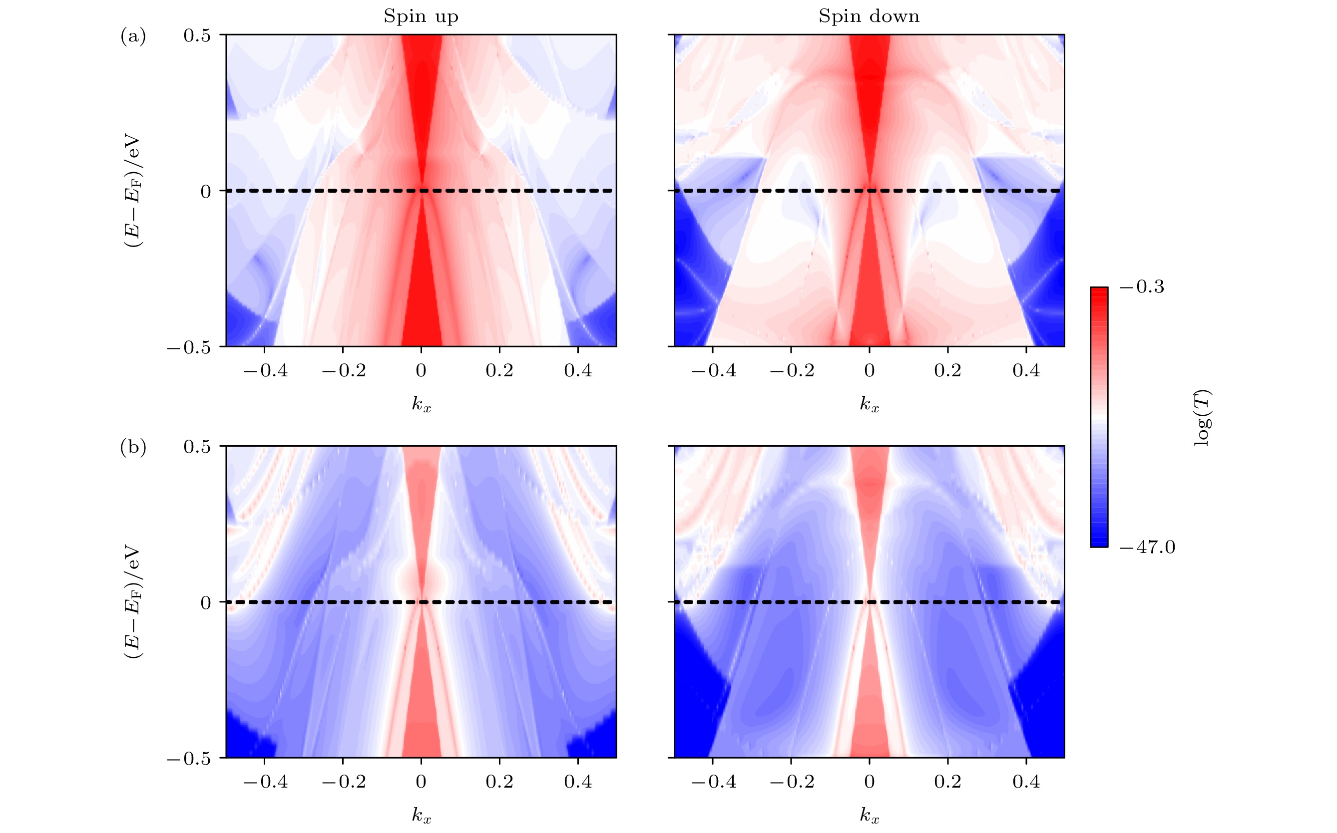 图 3 (a)透明接触器件和(b)隧穿接触器件的透射谱, 其中左边一列是自旋向上通道的透射谱, 右边一列是自旋向下通道的透射谱
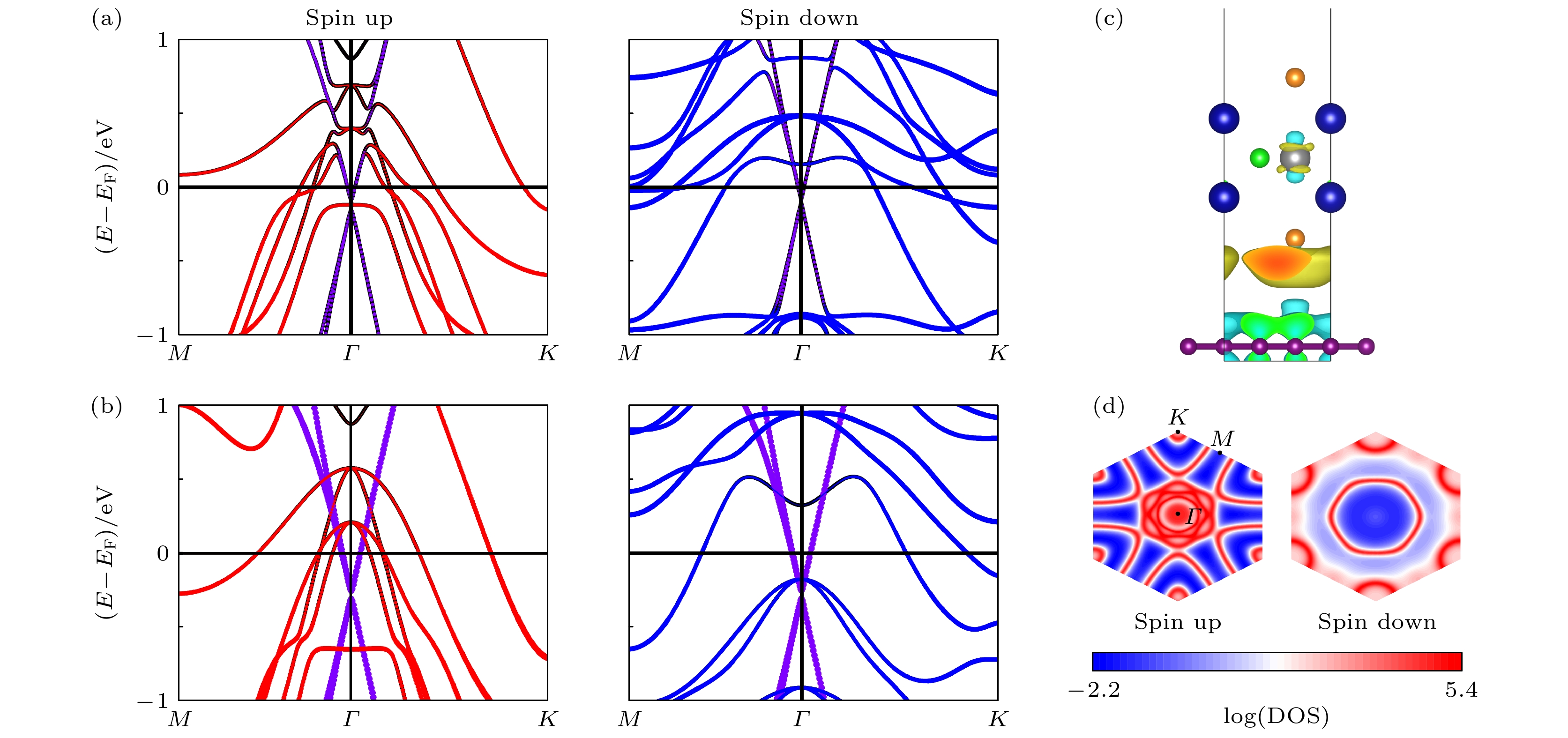 图 4 (a) Fe3GeTe2/石墨烯异质结能带; (b) Fe3GeTe2/氮化硼/石墨烯异质结能带; (c) Fe3GeTe2/石墨烯异质结差分电荷密度, 其中绿色代表电子损耗, 黄色代表电子积聚; (d) 费米能级上k点依赖的Fe3GeTe2态密度分布; 图4(a) 和图4 (b) 中左边一列为自旋向上能带, 右边一列为自旋向下能带