全文HTML
--> --> -->超快激光与物质的相互作用, 可以激发固体内部的准粒子产生新奇的光学或电学效应. 例如, 时间分辨抽运-探测方法研究激发态准粒子的超快动力学, 包括非常规高温超导体[8-11]、强关联体系[12-14]、拓扑量子态[15-17]、半导体材料[18,19]等以及激光诱导及调控的电子相干性[20-24]、晶格相干性[15,16]、声波相干性[25]、自旋波量子压缩态[26,27]等. 激发光的偏振可用于产生和控制表面源自拓扑特性的自旋极化光电流[28-34](通常只有pA—nA[32-34]). 2012年, Mclver等[32]利用795 nm的激光对拓扑绝缘体Bi2Se3进行探测, 成功观察到了源于拓扑绝缘体表面态贡献的光电流, 并发现改变光的偏振方向会逆转光电流的方向. 2017年, 他们还使用中红外激光(10.6 μm)成功探测了拓扑半金属TaAs[33]中的光电流, 并分辨了外尔费米子的手性. 2019年, Ma等[34]在二类外尔半金属TaIrTe4中采用中红外激光(4 μm)观测到了较强的圆偏振光调控的光电流响应. 拓扑半金属MoP内部具有三重简并费米子的自旋状态, 光电流可以在其拓扑表面产生或控制自旋极化电流.
本文设计并搭建了激光产生并调控电流的实验装置, 在Bi2Se3中成功探测到了对激光偏振依赖的光电流的变化. 采用上述装置, 用400 nm圆偏振激发光对MoP进行了光电流的探索, 以期激发及表征其三重简并费米子的手性特征或奇异表面态性质. 观测到了不同空间位置不随激发光偏振变化的电流信号, 判断其并非光电流而是热电流, 分析总结了MoP中没有产生光电流的原因. 本文的实验探索为研究更多的拓扑半金属和拓扑绝缘体材料的光电流响应提供了有益的借鉴, 为拓扑材料的光生热电流等的潜在应用提供了重要的物性基础.
2.1.光电流的实验测量
采用中心波长为800 nm, 重复频率为250 kHz, 脉宽为70 fs的掺Ti-蓝宝石飞秒激光光源以及倍频后的400 nm光源进行光电流实验. 实验装置如图1(a)所示, 800 nm (或经过BBO晶体倍频后的400 nm)超快激光脉冲经过偏振片后, 再通过旋转后面的λ/4波片的角度周期性地改变出射光的偏振类型(左旋光-线偏振光-右旋光). 最后入射光经过采样频率为1 kHz的斩波器调制后由焦距为10 cm的凸透镜聚焦到样品表面, 光斑直径大小为60 μm. 由于光激发的电流信号非常小, 通常在pA至nA量级[32-34], 需要在样品上制备两个电极接至前置放大器上将电流放大, 最终再通过锁相放大器按照斩波器的采样频率进行采集记录, 获得光电流的信号. 采用电动旋转装置精确调节λ/4波片旋转的角度θ, 由自行编制的LabVIEW软件对其进行控制. 图1(b)为引文[35]报道的MoP的能带结构, 用粉红色和蓝紫色箭头分别表示800 nm (1.55 eV)和400 nm (3.1 eV)激光脉冲激发电子可能产生光电流的区域. 图1(c)为引文[35]报道的三重简并点, 是图1(b)的局域放大图. 红色圆圈为4个三重简并点.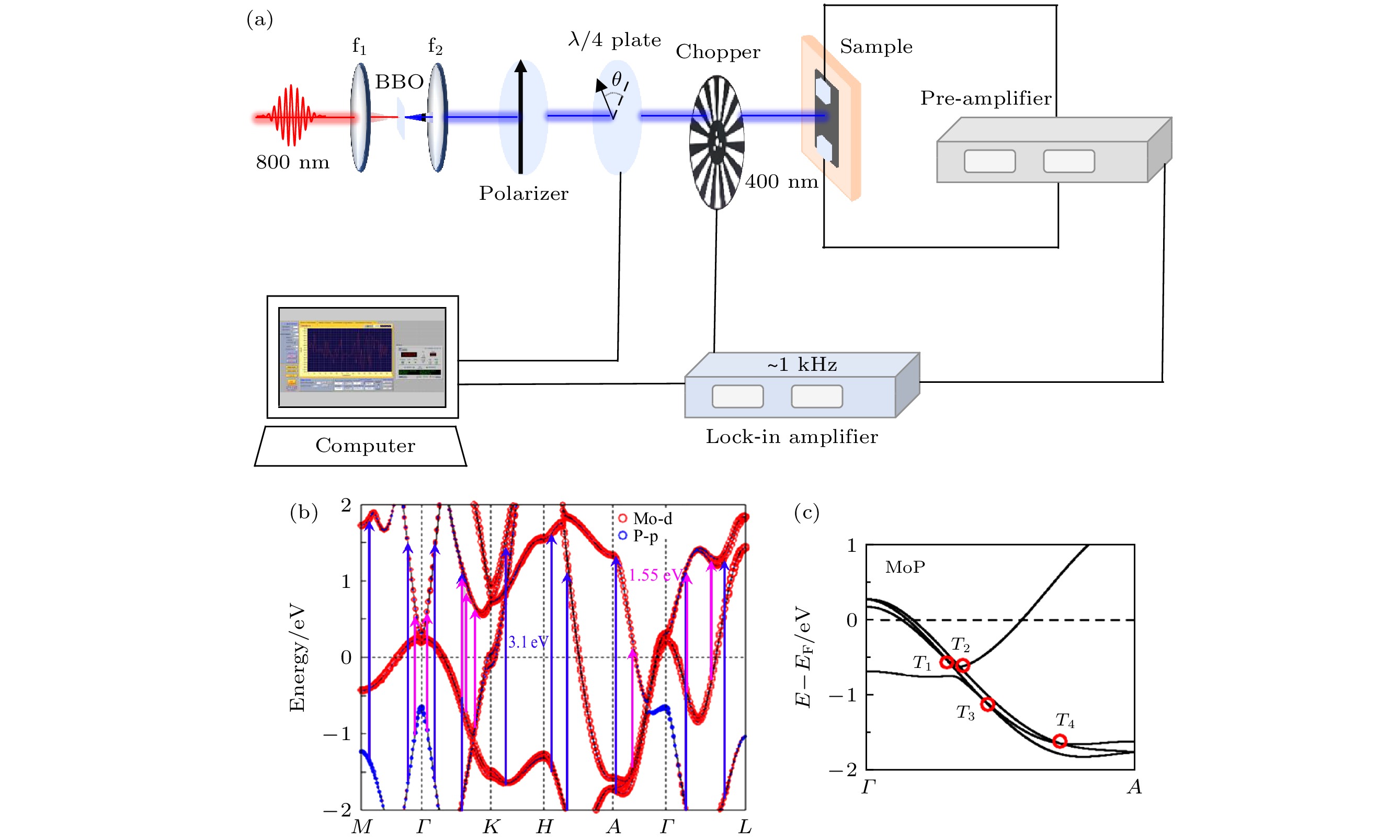 图 1 (a) 光电流产生和探测实验装置, f1和f2为透镜, BBO为倍频非线性晶体; (b) 800 nm (1.55 eV, 粉红色箭头) 和 400 nm (3.1 eV, 蓝紫色箭头) 脉冲激光可能激发的动量区域, 其中能带结构引自文献[35]计算结果; (c) MoP中的4个三重简并点局域放大(红色圆圈)[35]
Figure1. (a) Schematic photocurrent experimental setup. f1 and f2 are focusing lenses. BBO is the doubling frequency nonlinear crystal; (b) the allowed excitation areas by 800 nm (1.55 eV, pink arrows) and 400 nm (3.1 eV, purple arrows) pulsed lasers, respectively. The band structure is adapted from Ref. [35]; (c) the four triple points are highlighted by the red circles[35].
2
2.2.样品的表征
MoP的单晶通过固相反应合成, 样品制备详情见文献[5]. 用扫描电子显微镜(scanning electron microscopy, SEM)观察样品表面, 图2(a)展示了样品整体的SEM扫描图像, 图2(e), (f)分别展示了样品在5和20 μm分辨率下的SEM扫描图像, 大小约为1 mm × 1 mm, 样品厚度为162 μm, 其表面非常平整, 适合用于光电流实验及其他表征. 图2(a)右图展示了样品加上两个电极后底部通过低温胶粘在铜托上的实物图, 两根直径为20 μm的Pt丝的一端通过银胶粘在样品两侧的表面上, 另一端连接到外电路上.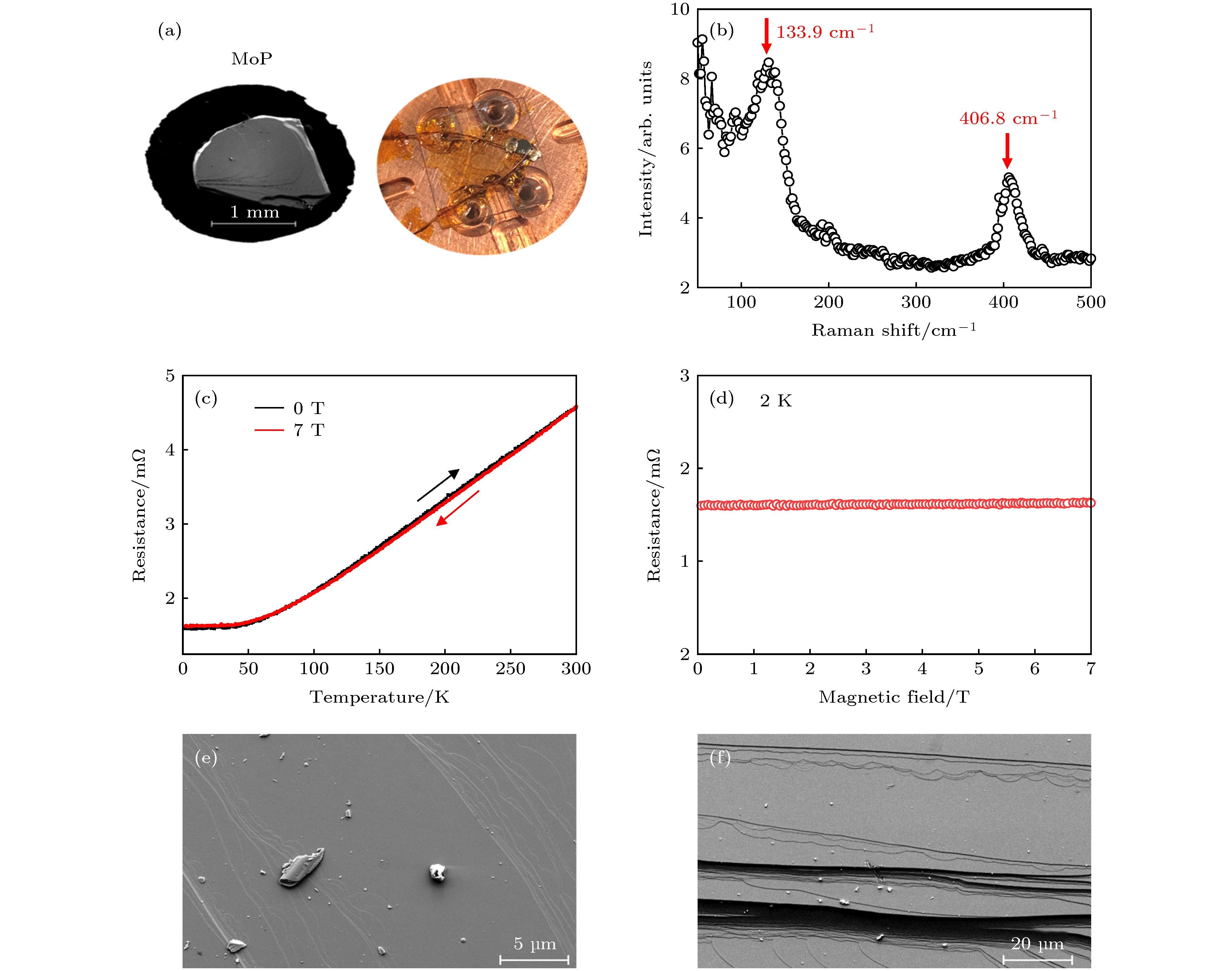 图 2 MoP样品的表征 (a) 光电流实验所使用的MoP样品, 左图为SEM图像, 右图为加电极后粘到铜托上的样品实物图; (b) 常温下的Raman光谱, 红色箭头标出两个拉曼峰; (c) 0和7 T下的电输运测量; (d) 2 K温度下的电阻随磁场的变化; (e) 5 μm分辨率样品局部放大SEM图; (f) 20 μm分辨率样品局部放大SEM图
Figure2. Characterizations of the MoP sample in the photocurrent experiment: (a) SEM image (left panel) and the sample after adding the electrodes (right panel); (b) Raman spectroscopy at room temperature, two red arrows mark the Raman peaks; (c) temperature dependence of the resistance at 0 and 7 T external magnetic field; (d) magnetic field dependence of resistance at 2 K; (e) SEM image with a resolution of 5 μm; (f) SEM image with a resolution of 20 μm.
对样品进行了Raman和输运表征. 图2(b)为MoP样品的Raman散射光谱, 采用532 nm波长、0.9 mW功率的线性偏振连续激光作为光源进行了近场共聚焦拉曼光谱测量, 透过一个50× 的物镜汇聚到样品表面, Raman光谱的分辨率为2 cm–1. 从获得的Raman光谱中可以看到, 在133.9和406.8 cm–1处各出现了一个Raman峰, 尚未发现有关MoP的详细的Raman研究工作被报道. 图2(c)为MoP在0和7 T磁场下进行的电输运测量, 其中黑色曲线为不加磁场时的数据(黑色箭头表示升温过程), 红色曲线为7 T磁场下的测量数据(红色箭头表示降温过程). 由图2(c)中曲线可以看出, 在有无磁场条件下, 电阻率随温度的变化曲线基本重合, 均在大约50 K附近出现转折. 说明磁场不会对MoP的输运特性产生影响. 在0 K时电阻率不为0, 经计算剩余电阻率(residual resistance ration, RRR)大约为RRR = R300 K/R2 K = 2.87; 与文献[35]的结果趋势相似, 仅 RRR有些差异, 可能与样品生长条件不同、掺杂浓度不同、电极接触电阻、或样品表面有氧化等有关. 图2(d)所示为MoP在2 K温度下测得的电阻随磁感应强度的变化曲线, 图2(d)中显示其电阻随磁场基本不变; 这也与文献[35]报道的数值有较大出入, 可能是同样原因造成, 或者系不同样品三重简并点离费米面距离不一样所致.
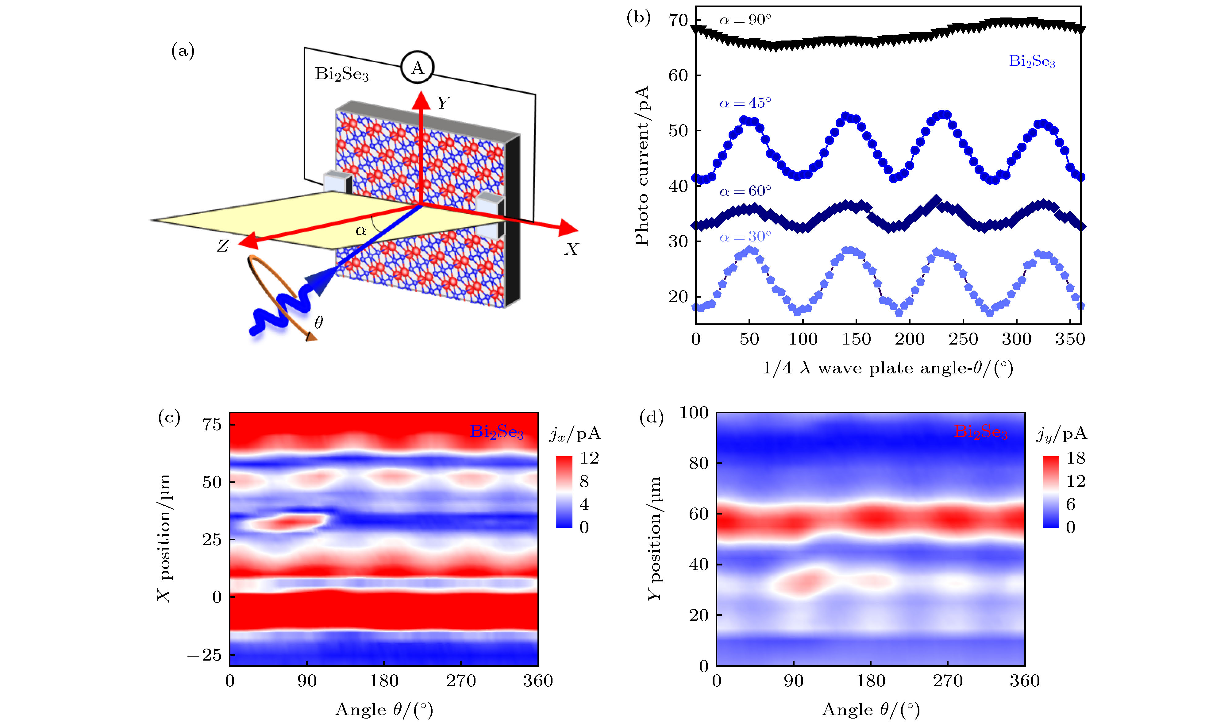 图 3 (a) 光电流实验示意图; (b) 不同入射角情形下Bi2Se3样品的光电流强度对激发光圆偏振度的依赖关系(有offset); (c) 光45°入射Bi2Se3样品情形下, 扫描X方向位置, 光电流强度对偏振的依赖关系图; (d) 光45°入射Bi2Se3样品情形下, 扫描Y方向位置, 光电流强度对偏振的依赖关系图
Figure3. (a) Schematic of the experimental geometry; (b) photocurrent intensity depending on the polarization of the laser beam under different incident angles, which is offset for clarity; (c) photocurrent intensity depending on the sample position along the X axis, where the incident angle of ultrafast pulses is 45°; (d) photocurrent intensity depending on the sample position along the Y axis, with 45° incidence angle.
接下来分别采用800和400 nm的激发光对MoP样品进行了类似的光电流实验. MoP的晶体结构如图4(a)所示, 其空间群为

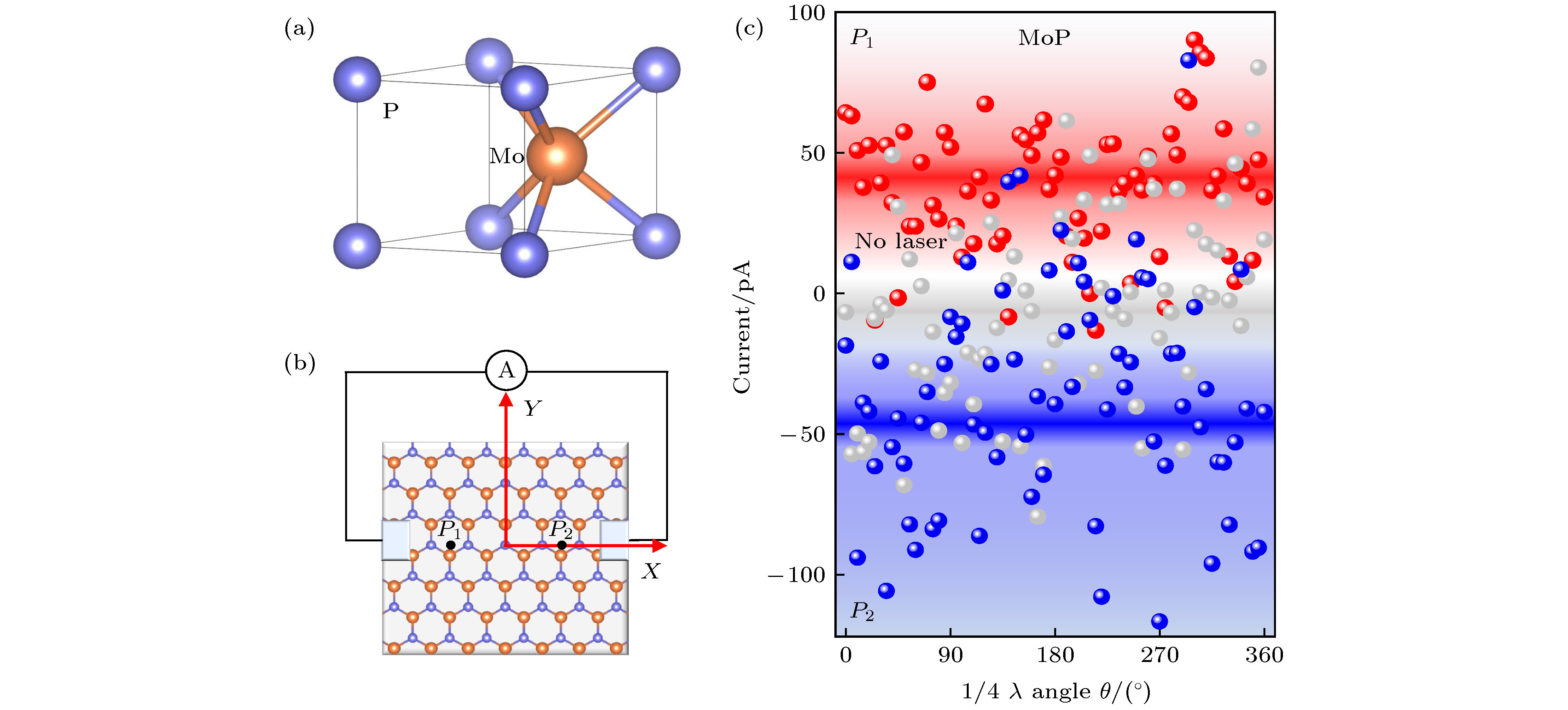 图 4 (a) MoP样品的晶格结构示意图; (b) 光激发样品的光斑位置示意图; (c) 400 nm超快激光照射MoP样品的P1和P2两个对称位置时, 分别测得的电流随偏振的依赖关系. 红色和蓝色代表P1和P2两个位置, 灰色为不加光照射时测得的电流
Figure4. (a) Schematic lattice structure of MoP, purple and brown spheres represent P and Mo atoms, respectively; (b) schematic diagram of the experiment illustrating the two photoexcitation positions on the sample; (c) polarization dependence of the current intensity at P1 and P2 under 400 nm light excitation. Solid dots in red and blue are current intensity data obtained at P1 and P2, respectively. Gray dots donate the situation without any light excitation.
分析在实验中未能在MoP单晶中观测到偏振依赖类型的光电流可能的原因有: 1) 虽然能量匹配, 但是其中只有很小一部分是直接或间接激发了三重简并点附近的电子, 在这一小部分电子中可能有一部分在室温下失去了拓扑特性, 剩余的部分自旋还受扩散等因素影响使得自旋寿命为有限, 最终的效果是使得探测光电流很具挑战性; 2) 电极制作技术不够精密, 接触电阻太大, 使得信号被淹没在背底之中, 但从较为成功的Bi2Se3对比实验看来, 这方面的影响并不是决定性的; 3) MoP的表面存在杂质或者已经氧化; 4) 在该体系中, 外尔锥或三重简并锥不够倾斜, 不同的外尔锥附近的光激发载流子产生的电流相互抵消, 总的净电流为0. 针对以上可能的原因, 为了进一步探测该体系中的光电流响应, 对于实验的方案进行了改进, 包括: 1) 选取更为合适的激发波长, 例如中远红外、THz波段等, 但此方法面临拓扑量子态深埋于费米面以下等挑战; 2)对样品电极制备进行更为精密的微加工处理, 进一步减小接触电阻; 3) 对样品表面进行抛光处理, 必要情况下尝试进行原位生长测量; 4) 增加对样品的外场调控, 诸如磁场、应力场等.
