全文HTML
--> --> -->表面等离激元(surface plasmon polaritons, SPP)是电磁波与金属表面自由电子耦合而形成的一种沿金属表面传播的近场电磁波. 它能将入射光波局域到亚波长尺度进行传播, 从而能极大地减小光学元件的尺寸, 便于光学集成. 此外, 由于光波的亚波长局域, 可以实现光波的近场增强, 这在增强光学非线性、光与物质作用方面有着非常重要的应用. 金属-电介质-金属(metal-dielectric-metal, MDM)波导是被广泛研究的SPP波导结构. 由于电磁场能量在电介质层中高度局域, 有望实现芯片级的光互联. 因而, 基于MDM结构的各种光功能器件是目前研究的热点. 2014年, Zhang等[5]将梳状线槽和矩形腔置于金属包层内, 利用它们之间的耦合得到明暗状态, 在明态和暗态之间进行相消干涉从而实现EIT效应. 目前, 在MDM波导中实现EIT现象主要有两种途径: 第一种, 在MDM波导结构中添加凹槽, 这样可使入射波在槽中干涉形成EIT, 并且随着凹槽数量的增加, 透射峰的数量也会增加[6], 但在凹槽中形成的法布里-珀罗共振模式(Fabry–Pérot mode, FP)会使得透射峰的强度下降; 第二种是类似于电介质波导-微腔结构, 波导与微腔之间通过倏逝波耦合, 实现EIT现象[7,8], 这需要精确控制波导与金属微腔的间距, 但波导与金属微腔的间距很小, 会使得加工成为一个难题.
本文提出一种金属-电介质-金属波导侧边耦合金属微腔的设计方案. 不同于常用的倏逝波耦合方案, 结构中波导与微腔间引入开口狭缝, 通过控制开口狭缝的宽度和偏离位置, 来调制微腔中模式的泄漏率, 从而影响波导模式与微腔模式以及微腔模式间的耦合效率, 进而对结构中类EIT窗口的峰值和半高全宽(full width at half maximum, FWHM)进行调制. 通过频域有限差分方法(finite-difference frequency domain, FDFD)对结构的性能进行模拟仿真和优化, 通过时域耦合模理论(temporal coupled mode theory, TCMT)对结构类EIT形成的机理进行了解释.
本文的结构如下: 第2节, 简要介绍了单个波导-微腔结构, 分析了其微腔的模式特性以及结构的透射特性; 第3节, 分析了波导-双微腔结构, 通过开口狭缝调制微腔中高Q模式与低Q模式间的耦合, 在结构透射谱中实现了类EIT效应. 通过TCMT对类EIT的形成机制进行解释, 利用FDFD方法对类EIT窗口进行了优化. 最后是结论部分.
 图 1 单个金属波导-微腔侧边耦合结构. 银-空气-银构成一个高局域的MDM波导结构, 空气层厚度为wd, 金属微腔的长度为L, 宽度为D. 波导与微腔间通过开口的狭缝进行耦合, 狭缝的宽度为C, 高度为S, 狭缝中心与微腔中心的偏移量为dsp
Figure1. The schematic diagram of single metal waveguide-cavity side-coupled structure. The MDM waveguide is consisted by silver-air-silver. The width of air layer is wd. The length and width of metal microcavity are L and D, respectively. A slit is used to connect the waveguide and microcavity. The width and height of slit are denoted as C and S, respectively. The center-to-center distance between slit and cavity is denoted as dsp.
这里通过FDFD方法来模拟结构的电磁特性. 空气波导层的厚度wd = 200 nm, 在工作波长1500 nm附近, 波导结构仅支持单个SPP模式. SPP模式通过总场-散射场的形式引入到结构中[9]. 模拟中, 离散网格的尺寸为5 nm, 金属银的介电函数来自于实验值[10]. 本文中, 波导与微腔的间距远大于电磁波在金属中的穿透深度. 微腔不是通过波导的倏逝波耦合激发[11], 而是通过开口狭缝的能量泄漏来激发[12,13], 因而狭缝的宽度(C )和位置偏移量(dsp)将直接影响结构的光谱响应. 图2(a)给出了在固定狭缝偏移量(dsp = 120 nm)时, 不同狭缝宽度对应的结构透射谱. 可以看出, 由于存在狭缝, 波导中的电磁能量能有效耦合到金属微腔中, 形成谐振, 从而会在透射谱中形成低谷. 随着狭缝宽度的增加, 微腔中更多的电磁能量会泄漏出来, 使得模式的损耗增加, 因而透射谱的FWHM会展宽. 而且狭缝宽度的增加, 会对微腔中模式谐振频率进行修正, 结构的透射谱的低谷会蓝移. 结构谐振时相应的品质因子(Q值)在图2(b)中给出. 随着金属狭缝宽度的增加, 结构的共振Q值减小. 金属狭缝宽度C = 70 nm, 高度S = 200 nm和偏移量dsp = 120 nm时, 结构谐振时对应磁场的振幅分布(|Hy|)在图2(b)的插图中给出. 可以看出, 微腔中激发一阶FP共振模式. 金属微腔中FP模式的谐振条件表示为[14]
 图 2 狭缝偏移位移固定(dsp = 120 nm), 不同狭缝宽度情况下 (a) 结构的透射谱; (b)结构共振Q值的变化情况. 结构谐振时, 对应的磁场振幅分布(|Hy|)也在图(b) 中给出. 狭缝宽度固定(C = 100 nm), 不同狭缝偏移量情况下, (c) 结构的透射谱; (d) 结构共振Q值的变化情况. 微腔的尺寸(长L = 650 nm, 宽度D = 200 nm), 波导的宽度wd = 200 nm
Figure2. As the location offset of slit is fixed (dsp = 120 nm), (a) the transmittance spectra of structure with the different width C, (b) the Q factor of structure versus the width C. The amplitude distribution of magnetic field at the resonant wavelength of structure with width C = 100 nm is also shown in the inset of Fig. 2(b). (c) The transmittance spectra of structure with the different location offset dsp; (d) the Q factor of structure versus the dsp. The length and width of microcavity are L = 650 nm and D = 200 nm, respectively. The thickness of waveguide wd = 200 nm.
因此, 通过调节狭缝的开口宽度或者偏移位置, 可以改变微腔中模式的泄漏率, 从而实现对SPP入射的波导-微腔结构的共振特性进行调制, 这不同于通过倏逝波耦合的波导-微腔结构, 在其结构中是通过调节谐振腔与波导的几何间距来实现的.
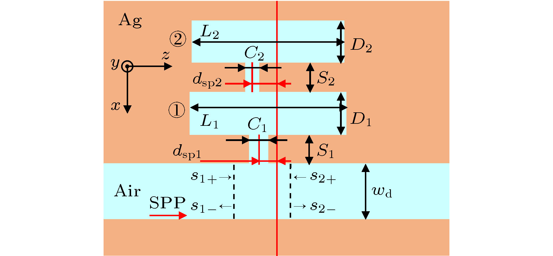 图 3 金属波导-双微腔侧边耦合结构示意图. 在图1的基础上再加入一个谐振腔, 并为两个谐振腔编号为①与②. 靠近波导的为1号微腔, 所有的结构参数的尾数都为1; 远离波导的为2号谐振腔, 所有的结构参数的尾数为2. 空气层厚度为wd
Figure3. The schematic diagram of metal waveguide-double microcavities side-coupled structure. A other microcavity is introduced into the structure shown in Fig.1. The two microcavities are numbered as ① and ②, respectively. The width of air layer is wd.
如图3所示, 第一个微腔的宽度和长度分别表示为D1与L1, 微腔与波导间的开口狭缝的高度与宽度分别表示为S1与C1, 狭缝中心与结构中心的偏移量表示为dsp1. 第二个微腔的宽度与长度分别表示为D2与L2, 两个微腔间通过开口狭缝连接, 连接狭缝的高度与宽度分别表示为S2与C2, 狭缝中心与结构中心的偏移量表示为dsp2.
结构中的电磁共振行为, 可以通过时域耦合模理论(TCMT)来描述. 结构的TCMT模型也在图3中给出, 1号腔与波导的连接狭缝的左端为入射面, 模式间的动力学方程表示为[15-17]:


 图 4 波导-双微腔结构的透射谱. 其中, 红色实线表示FDFD方法得到的结果, 蓝色圆点为TCMT方法得到的结果. 为了便于比较, 单个波导-微腔结构的透射谱在图中以黑色虚线表示; (b)波导-双微腔结构中, 透射波的位相变化情况. 数值模拟中, 结构的几何参数为L1 = 650 nm, D1 = 200 nm, S1 = 200 nm, C1 = 100 nm, dsp1 = 120 nm, L2 = 625 nm, D2 = 200 nm, S2 = 250 nm, C2 = 40 nm, dsp2 = 80 nm, wd = 200 nm.
Figure4. (a) The transmittance spectra of waveguide-microcavities structure. The red line and blue dotted line denote the results obtained from FDFD simulation and TCMT, respectively. For comparison, the transmittance spectra of the single waveguide-microcavity are shown with black dashed line; (b) for waveguide-microcavities structure, the phase of output wave versus the wavelength. In simulation, the parameters of structure are L1 = 650 nm, D1 = 200 nm, S1 = 200 nm, C1 = 100 nm, dsp1 = 120 nm, L2 = 625 nm, D2 = 200 nm, S2 = 250 nm, C2 = 40 nm, dsp2 = 80 nm and wd = 200 nm.
在图3所示的双金属微腔结构中, 由于存在开口狭缝, 波导与微腔、微腔与微腔间存在电磁能量泄漏, 泄漏的能量促使模式间进行耦合, 从而调节结构的输出波形. 结构中波导右侧的输出波主要来自于三部分的贡献: 第一部分来自于入射SPP的直接透射; 第二部分来自于第一个腔(低Q模式谐振)的直接泄漏辐射; 第三部分是耦合到第二个腔中的能量(高Q模式谐振)通过第一个微腔间接泄漏到波导中[5]. 当结构谐振时, 后面两部分能量的场振幅会发生干涉相消, 导致在原来透射低谷的位置上, 出现透射峰值, 实现了类似于EIT现象. 结构透射峰值对应的磁场分布在图4(a)中的插图中给出, 可以看出, 由于场振幅的干涉相消, 在第一个微腔中, 磁场振幅很弱. 图4(b)给出了透射SPP位相随波长的变化关系. 由于干涉相消的作用, 在结构的透射峰附近, 出射光的位相会有剧烈的变化, 这在慢光效应中有着重要的应用[20].
在图3所示的结构中, 开口宽度C1与偏离dsp1主要决定了共振峰的主线形, 而C2与dsp2影响耦合强度, 进而影响类EIT透射峰的品质因子. 所以为了探究结构参数对于类EIT线形的影响, 通过改变狭缝宽度C2的大小, 得到透射谱曲线中透射峰值大小以及FWHM的变化情况, 结果在图5中给出.
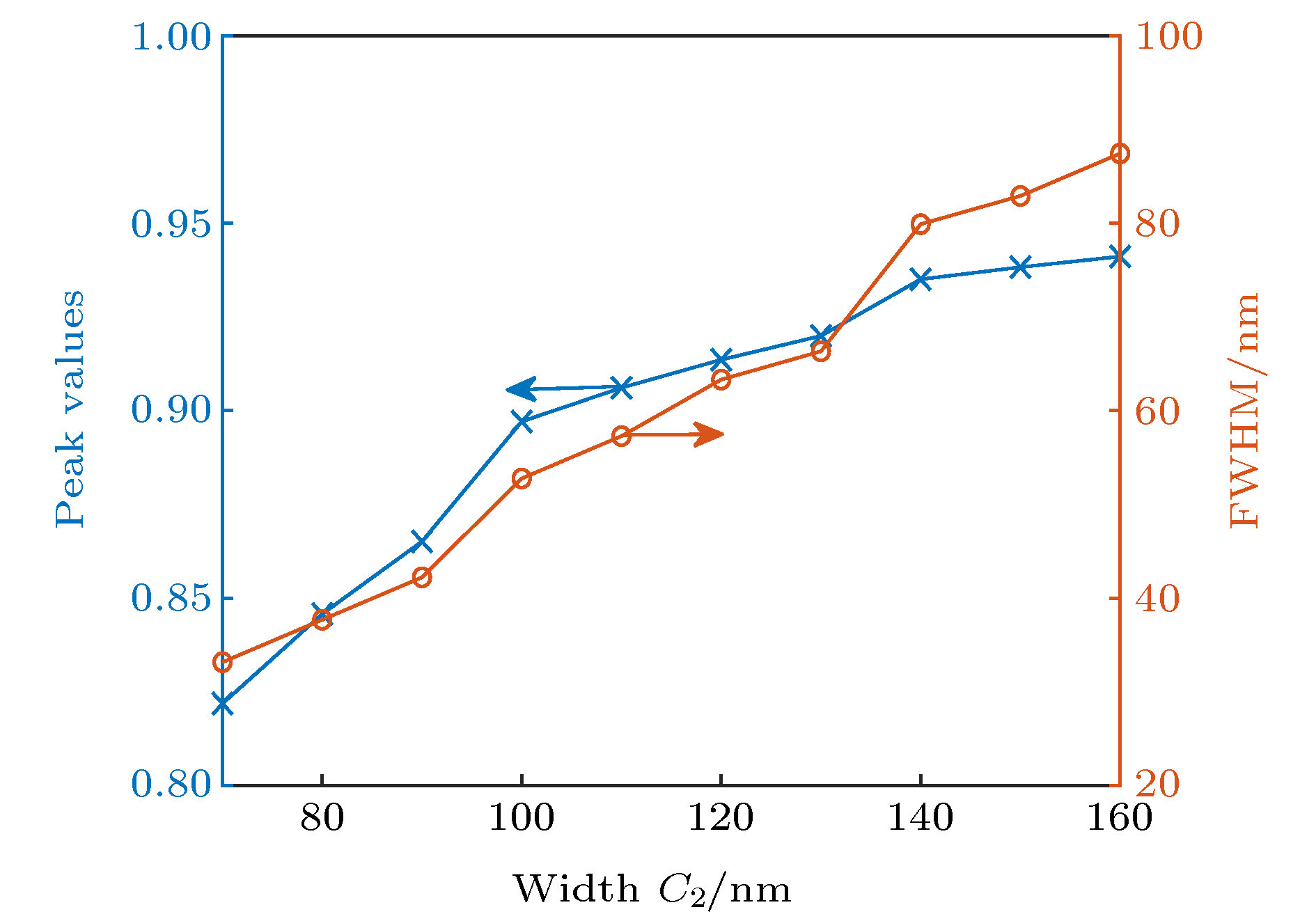 图 5 类EIT窗口透射峰值和FWHM与狭缝开口宽度C2的关系. 结构的其他参数为L1 = 650 nm, D1 = 200 nm, S1 = 200 nm, C1 = 100 nm, dsp1 = 120 nm, L2 = 625 nm, D2 = 200 nm, S2 = 250 nm, dsp2 = 80 nm, wd = 200 nm
Figure5. The peak value of transmission and the FWHM of EIT window versus the width C2 of slit. In simulation, the geometrical parameters of structure are L1 = 650 nm, D1 = 200 nm, S1 = 200 nm, C1 = 100 nm, dsp1 = 120 nm, L2 = 625 nm, D2 = 200 nm, S2 = 250 nm, dsp2 = 80 nm and wd = 200 nm.
从图5可以看出, 当C2变大时, 峰值与半波全宽呈增加趋势, 从(2)式分析可以知道, 当开口变大时, 微腔中模式的泄漏率会增加, 导致两个微腔中模式间的耦合系数会变大, 这不仅使透射峰值变大, 同时还会拓宽EIT的透射窗口的宽度.
