Fund Project:Project supported by the National Natural Science Foundation of China (Grant Nos. 61871355, 61831012)
Received Date:07 October 2019
Accepted Date:05 November 2019
Published Online:20 January 2020
Abstract:The metamaterial absorber has the advantages of thin thickness, small size, simple structure and high absorption. As is different from the traditional metamaterial absorber, the adjustable material is used for designing the structure, which can realize the dynamic modulation of the device by changing the external factors without changing the device structure. In this paper, an adjustable terahertz absorber with multi-defect combination embedded VO2 thin film is proposed. It is composed of three layers: the upper metal pattern layer, the substrate and the bottom metal plate. Vanadium dioxide medium is sandwiched between the upper surface and the substrate. The absorption performance of the absorber composed of different defect combinations is studied, and the electric field distribution of each combination is analyzed. At the same time, the influences of defects on the absorption performance of the absorber are compared with each other and analyzed. After comprehensive analysis, the defects are combined into the final proposed structure, and the electric field distribution and surface current distribution are analyzed. The relevant parameters affecting the performance of the absorber are scanned and analyzed, and the final optimized structural parameters are obtained. The results show that the absorption rate at f = 4.08 THz and f = 4.33 THz are 99.8% and 99.9%, respectively. The phase transition of vanadium dioxide can be controlled by changing ambient temperature, so that the absorption rates of two frequency points can be changed from 99.8% to 1.0%. In addition, the surface normalized impedance of the proposed absorber is analyzed, which shows that the normalized surface impedance of the designed absorber matches the impedance of the free space well. By changing the incident angle and polarization of terahertz wave, the results show that the absorption rate of the absorber under TE and TM polarization wave both can be more than 98% with the incident angle ranging from 0° to 40°. The proposed terahertz wave absorber has the characteristics of high absorption, dynamic tuning and insensitive polarization. It has good application prospects in terahertz wave related fields such as detectors and stealth technology. Keywords:terahertz wave/ vanadium dioxide/ multi-defect combination/ terahertz absorber
图 3 TE模式下电场E分布图 (a) 组合一, f = 4.06 THz; (d) 组合一, f = 4.27 THz; (b) 组合二, f = 4.03 THz; (e) 组合二, f = 4.33 THz; (c) 组合三, f = 4.06 THz; (f) 组合三, f = 4.39 THz Figure3. Electric field distribution in TE mode: (a) Combination 1, f = 4.06 THz; (d) combination 2, f = 4.27 THz; (b) combination 2, f = 4.03 THz; (e) combination 2, f = 4.33 THz; (c) combination 3, f = 4.06 THz; (f) combination 3, f = 4.39 THz.
图 4 多缺陷组合TE模式下电场E和电流A分布图 (a) f = 4.08 THz, 电场分布; (b) f = 4.33 THz, 电场分布; (c) f = 4.08 THz, 电流分布; (d) f = 4.33 THz, 电流分布 Figure4. Electric field and current distribution in TE mode with multiple defects: (a) f = 4.08 THz, electric field distribution; (b) f = 4.33 THz, electric field distribution; (c) f = 4.08 THz, current distribution; (d) f = 4.33 THz, current distribution.
对影响吸收频率点的重要参数进行扫描分析, 计算结果如图5所示. 从图5(a)中看出, 随着R增大, 低频率点发生蓝移, 吸收率也稍微降低. 当R = 8.5 μm时, 吸收器的吸收率最高, 达到99.2%; 当R = 9.0 μm时, 吸收器吸收率为98.9%; 当R = 9.5 μm时, 吸收器的吸收率为98.9%; 当R = 10 μm时, 吸收器的吸收率为98.8%. 在这个过程中发现吸收器的高频率点并没有发生明显的移动, 吸收率保持不变. 可以得出这样的结论, 缺陷十字架与中心距离R主要对吸收器的低频率点产生影响, 调节R大小, 可以实现吸收器的低频率点吸收率的优化. 此外, 本文还对缺陷圆环缺陷宽度W和中心圆环宽度D进行了仿真计算. 从图5(b)中可以看出, 缺陷宽度W对吸收器的低频率点几乎没有影响, 主要对吸收器的高频率点产生影响. W = 4.5 μm, f = 4.31 THz处吸收率为98.6%; W = 5.0 μm, f = 4.33 THz处吸收率为99.9%; W = 5.5 μm, f = 4.34 THz处的吸收率为99.0%; W = 6.0 μm, f = 4.35 THz处吸收率为97.6%. 可见随着W增加, 高频率点发生了蓝移. 中心圆环宽度D与吸收器吸收率的关系如图5(c)所示. 从图5(c)中可以观察到, 保持中心圆环圆心不变, 改变圆环宽度D从2 μm变化到4 μm, 吸收器在低频率点产生蓝移, 而高频率点产生红移, 且两个频率点上的吸收率均下降, 这是因为中心圆环宽度变化实际上改变了缺陷十字架与圆环之间间隙的宽度, 金属之间电磁共振强度也随着距离的增大而减弱, 当宽度D = 2.5 μm时, 共振强度最大, 吸收效果最好. 该吸收器优化得到的基本尺寸参数如下: 周期为40 μm, 顶层金属图案中缺陷圆环缺口宽度为W = 5 μm, 缺陷圆环宽度为2 μm, 其外半径为16 μm, 中心圆环宽度为D = 2.5 μm, 其外半径为8 μm, 缺陷十字架与单元中心位置距离为R = 8.5 μm, 缺陷十字架宽度为4 μm. 图 5 结构参数改变对应的吸收率曲线 (a) 缺陷十字架距离中心距离R; (b) 缺陷圆环缺陷宽度W; (c) 中心圆环宽度D Figure5. Absorption curves corresponding to the change of structural parameters: (a) Defect cross distance from center R; (b) defect ring width W; (c) center ring width D.
图 7 (a) 不同温度下吸收器的吸收率; (b) 吸收器的归一化表面阻抗 Figure7. (a) Absorption of the absorber at different tempera-tures; (b) normalized surface impedance of the absorber.

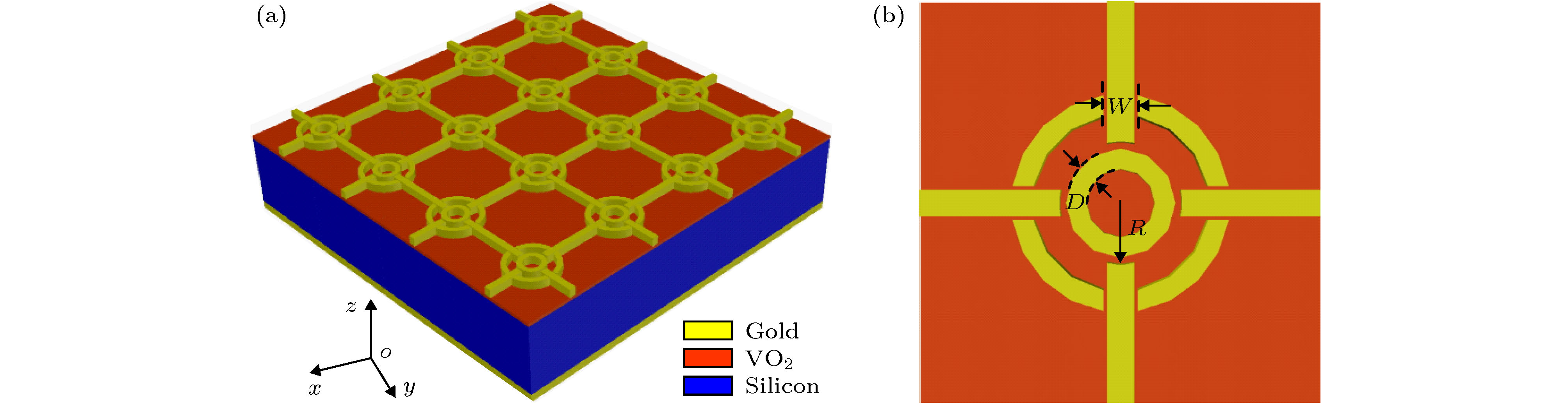 图 1 多缺陷组合结构可调太赫兹吸收器 (a) 单元结构三维立体图; (b) 单元俯视图
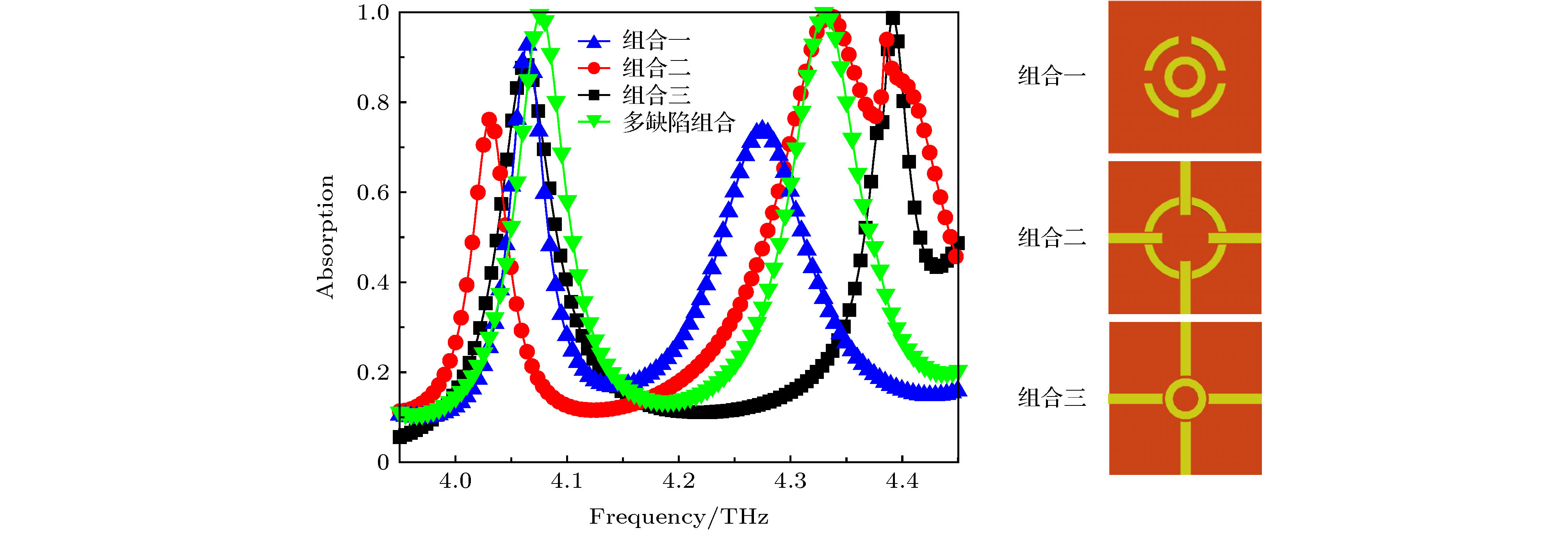 图 2 不同组合形成的吸收器吸收曲线
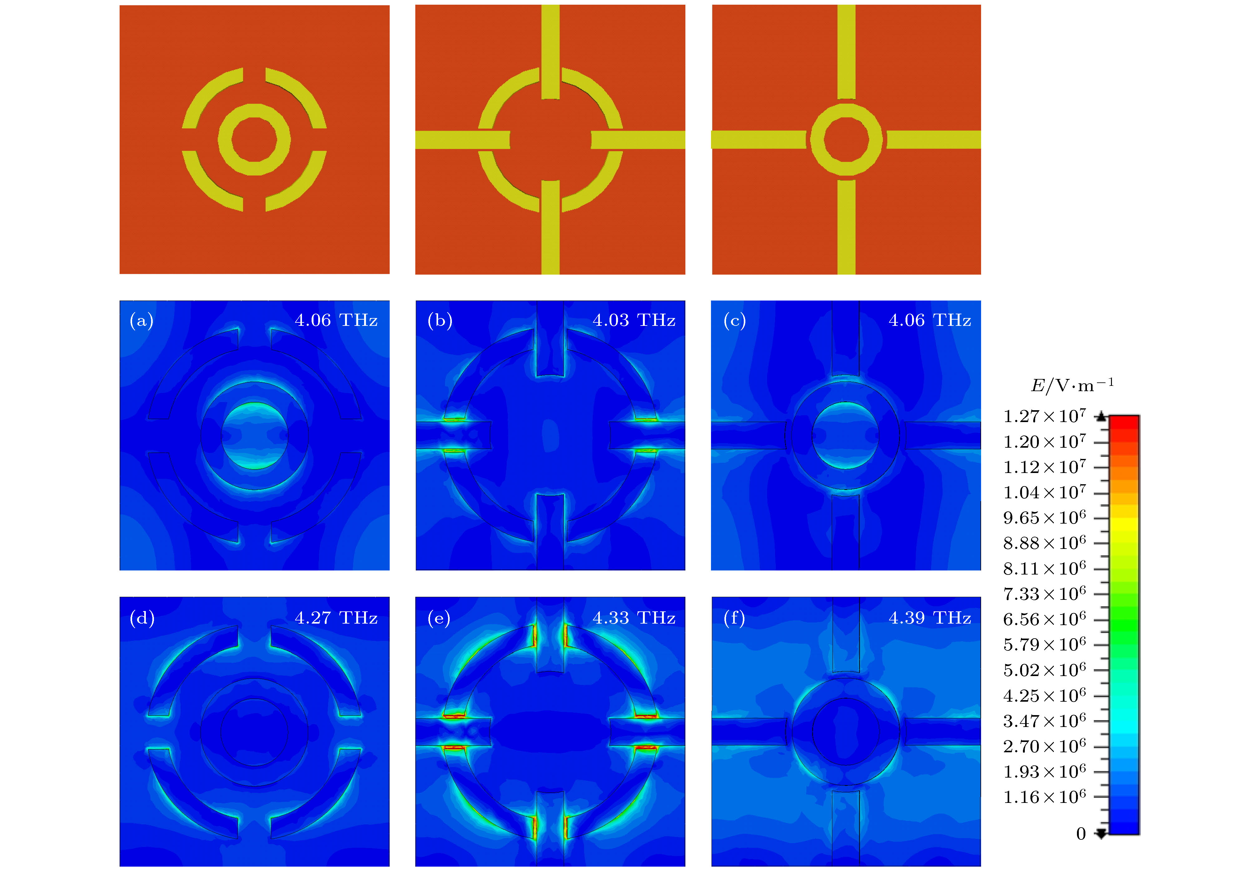 图 3 TE模式下电场E分布图 (a) 组合一, f = 4.06 THz; (d) 组合一, f = 4.27 THz; (b) 组合二, f = 4.03 THz; (e) 组合二, f = 4.33 THz; (c) 组合三, f = 4.06 THz; (f) 组合三, f = 4.39 THz
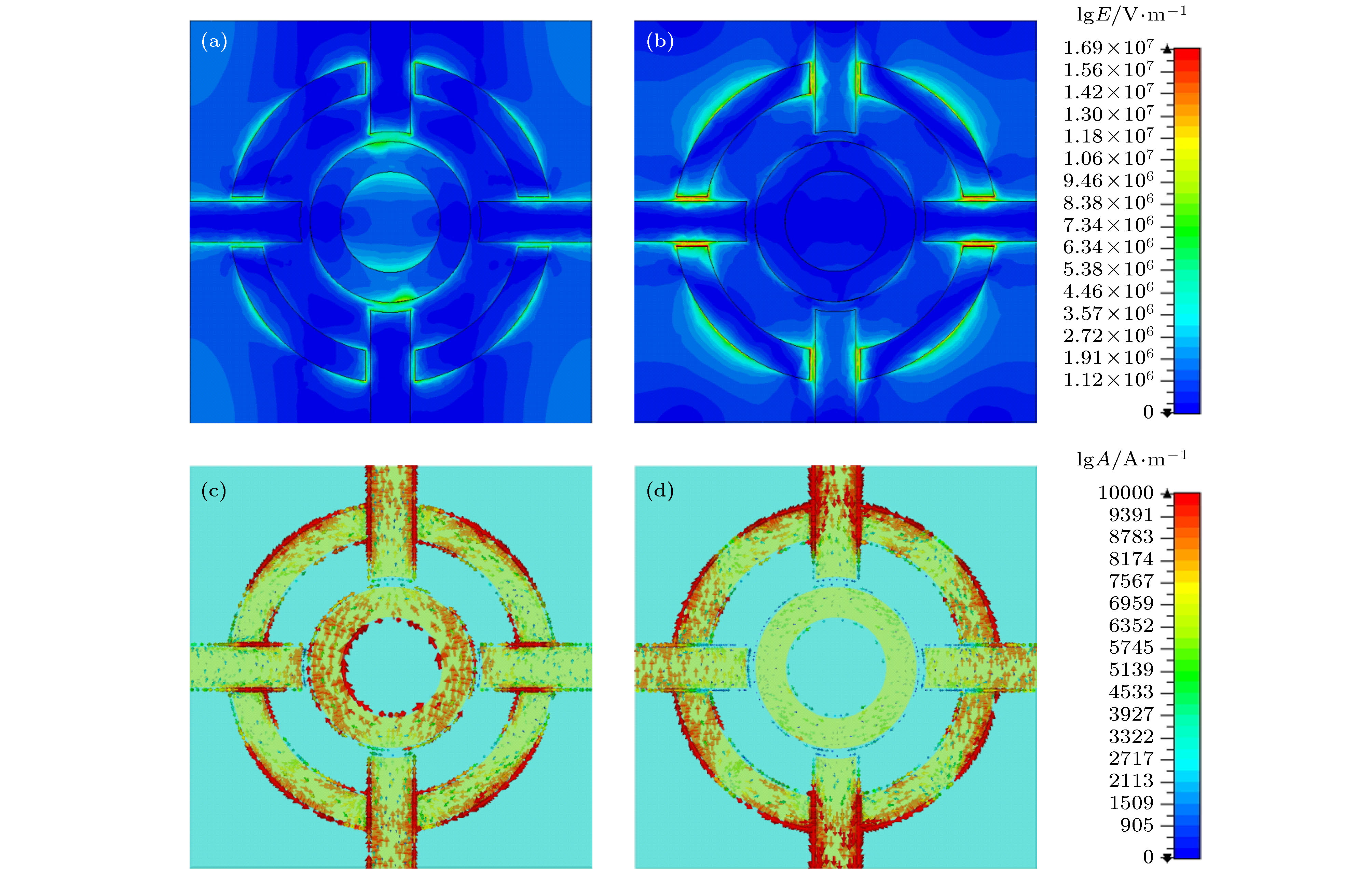 图 4 多缺陷组合TE模式下电场E和电流A分布图 (a) f = 4.08 THz, 电场分布; (b) f = 4.33 THz, 电场分布; (c) f = 4.08 THz, 电流分布; (d) f = 4.33 THz, 电流分布
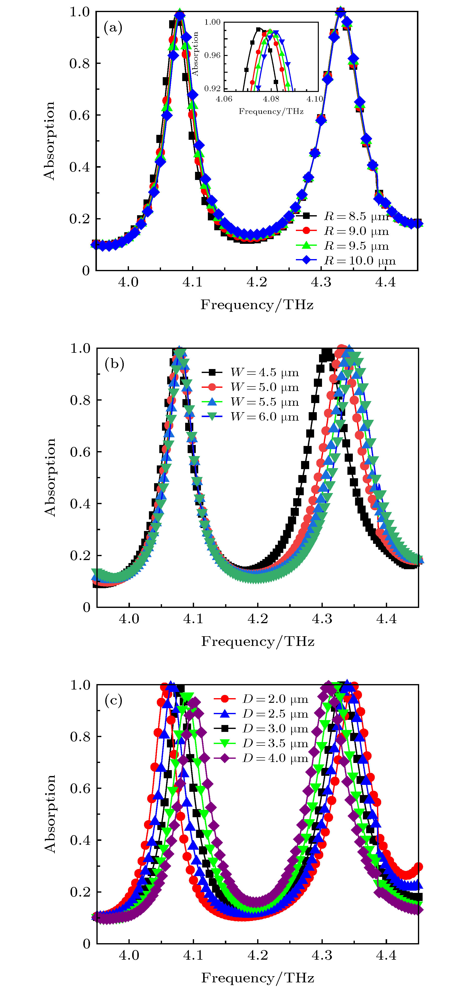 图 5 结构参数改变对应的吸收率曲线 (a) 缺陷十字架距离中心距离R; (b) 缺陷圆环缺陷宽度W; (c) 中心圆环宽度D


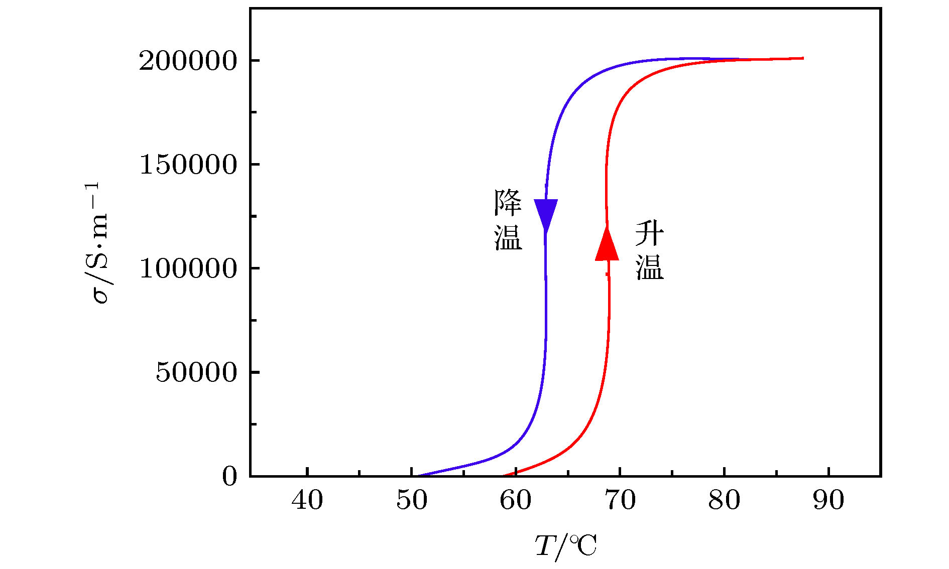 图 6 VO2的电导率随温度的变化
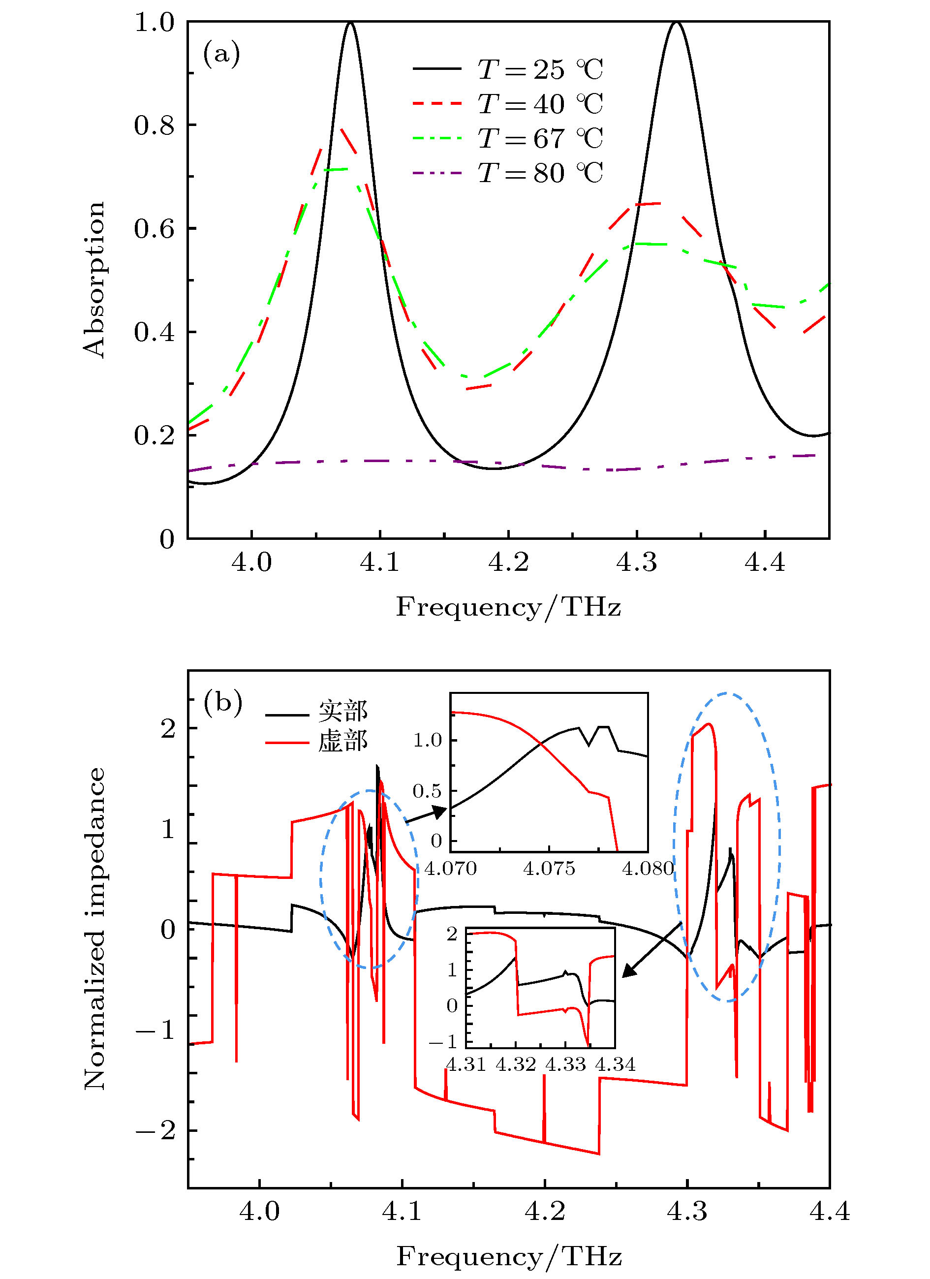 图 7 (a) 不同温度下吸收器的吸收率; (b) 吸收器的归一化表面阻抗
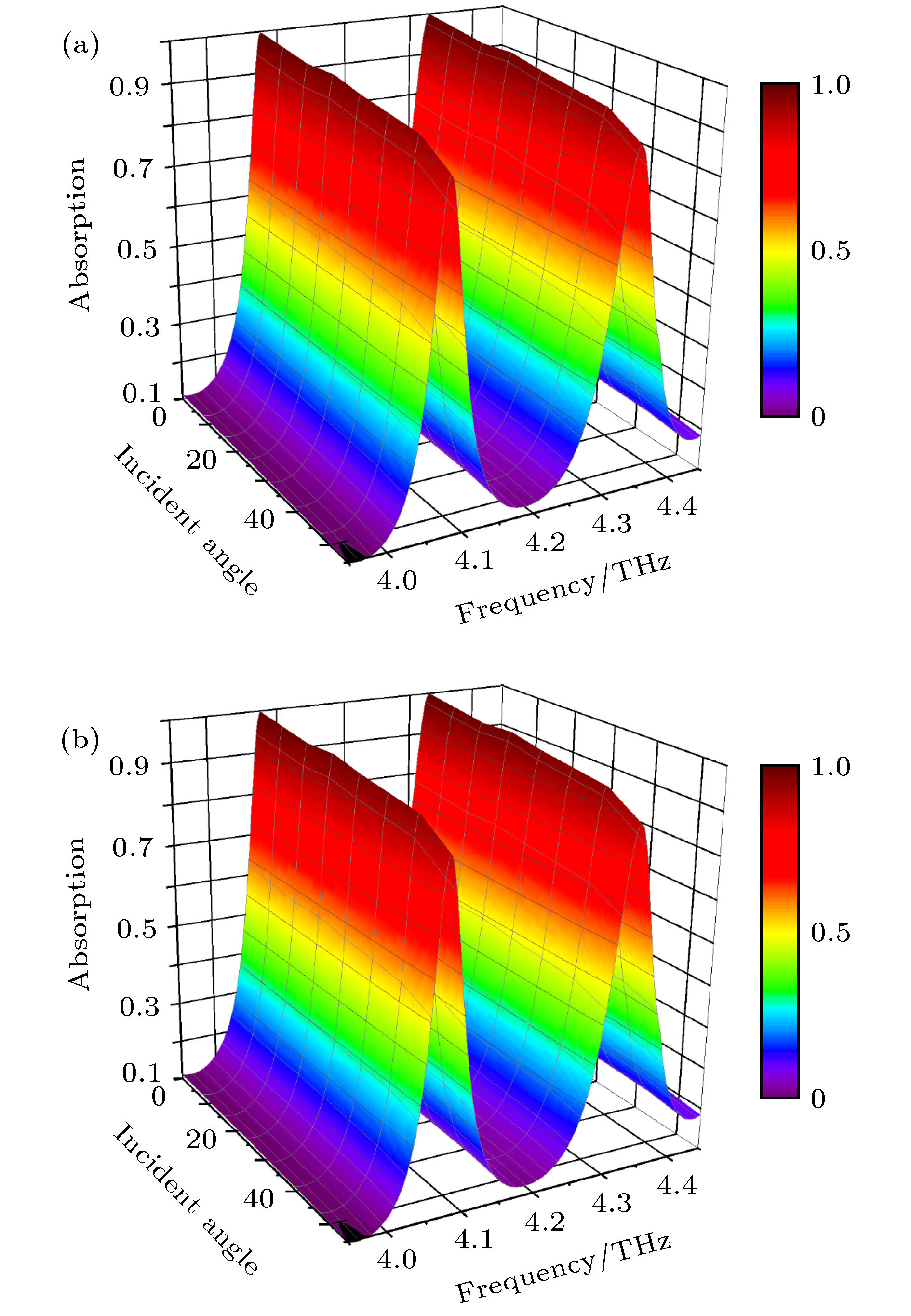 图 8 太赫兹吸收谱 (a) TE模式; (b) TM模式