全文HTML
--> --> -->通常, 台面刻蚀是实现氮化镓(GaN)基micro-LED器件间隔离的主要方法[14], 但台面刻蚀隔离不可避免地会引入侧壁刻蚀损伤, 同时产生侧壁悬挂键[15], 导致器件反向漏电流增大; 另一方面, 台面刻蚀还会引入深能级缺陷, 形成非辐射复合中心, 使器件非辐射复合速率增大、外量子效率降低, 从而减小器件有效工作面积 [16,17]; 并且随发光孔径的减小, 侧壁损伤对器件上述性能的影响更加显著, 因此侧壁损伤问题极大地限制micro-LED器件的发展与应用. 2012年, Tian等[18]研究micro-LED外量子效率与器件尺寸的关系, 研究表明小尺寸micro-LED器件在低电流密度下, 外量子效率主要受侧壁损伤的影响; 2017年, Hwang 等[19] 研究不同钝化方式对micro-LED器件的外量子效率影响, 发现通过原子层沉积(ALD)的方法生长SiO2钝化层可以有效减小侧壁损伤引起的漏电与非辐射复合, 从而增大了器件外量子效率. 鉴于常规台面刻蚀制备的micro-LED器件都存在严重的侧壁损伤, 所以有效降低或避免侧壁损伤的产生是提高器件性能的一个重要途径.
除了台面刻蚀隔离, 离子注入是目前实现GaN半导体器件有效隔离方法, 该方法已成功应用于高电子迁移率晶体管(HEMT)器件中[20]. 离子注入隔离是将具有一定能量的离子注入到GaN材料中, 可以精准地控制离子注入面积及深度, 引起GaN材料的晶格损伤, 并引入大量深能级缺陷, 降低注入区域载流子浓度[21,22], 形成可以达到电学隔离效果的高阻态区域. 与台面刻蚀隔离相比, 离子注入隔离为平面工艺, 可以避免侧壁损伤引入和侧壁悬挂键的产生, 减少侧壁非辐射复合中心和降低反向漏电流. 因此本文针对避免台面刻蚀造成的侧壁损伤, 提出一种通过氟(F)离子注入技术实现micro-LED阵列器件的新型制备方法.
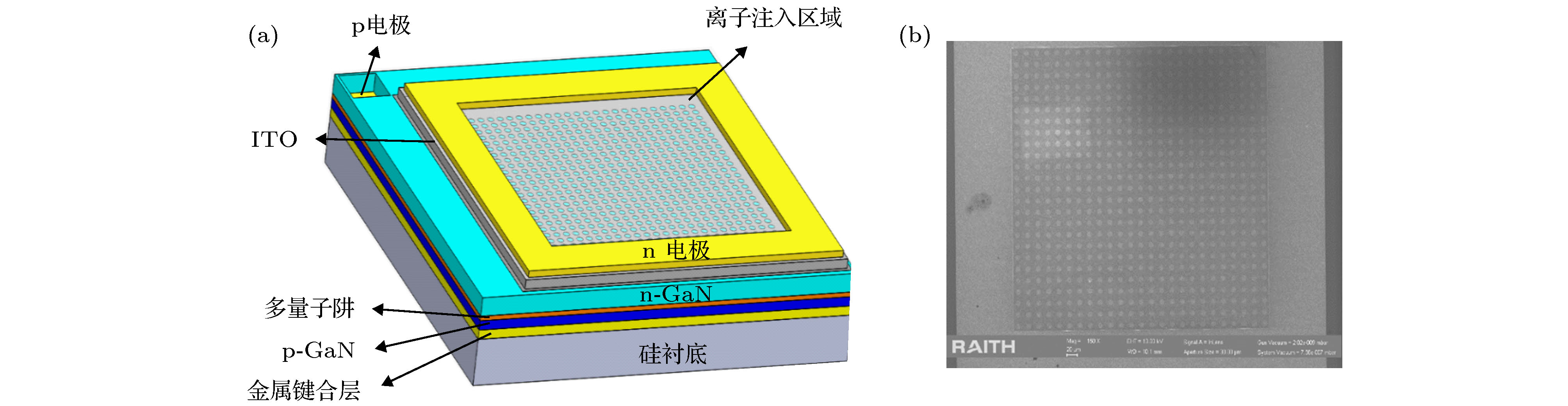 图 1 (a) micro-LED阵列结构图; (b) 10 μm micro-LED阵列表面SEM图像
Figure1. (a) Schematic structure of micro-LED array; (b) SEM image of 10 μm micro-LED array surface.
器件具体制备工艺流程如下: 首先通过倒装键合技术, 将LED外延片键合在硅(Si)衬底上, 并使用激光剥离蓝宝石衬底, 形成垂直结构LED; 然后利用感应耦合等离子体(ICP)刻蚀样品至n-GaN, 刻蚀出金属键合层, 将其作为micro-LED阵列p型电极; 随后通过F离子注入工艺对器件进行隔离, 样品A为单次注入, 注入能量为50 keV, 样品B为两次注入, 注入能量分别为50, 100 keV, 以10 μm阵列为例, 注入后样品扫描电镜(SEM)图如图1(b)所示; 最后在n-GaN表面沉积200 nm的ITO, 并在ITO上蒸镀Ti/Au(50/150 nm)金属作为n型电极, 并在氮气氛围下300 ℃退火2 min. micro-LED阵列样品的电流-电压(I-V)电学特性通过安捷伦高压探针台B1505A测试, 注入区域隔离区域方块电阻通过圆形传输线模型(CTLM)表征, 光输出功率通过积分球测试系统测得.
3.1.F离子注入能量对micro-LED阵列光电性能的影响
以6 μm发光孔径的micro-LED阵列器件为例, 在不同能量注入条件下, 其光电特性如图2所示, 图2(a)为器件I-V特性, 插图为样品半对数坐标下反向I-V特性曲线, 图2(b)为光输出密度-电流密度关系曲线.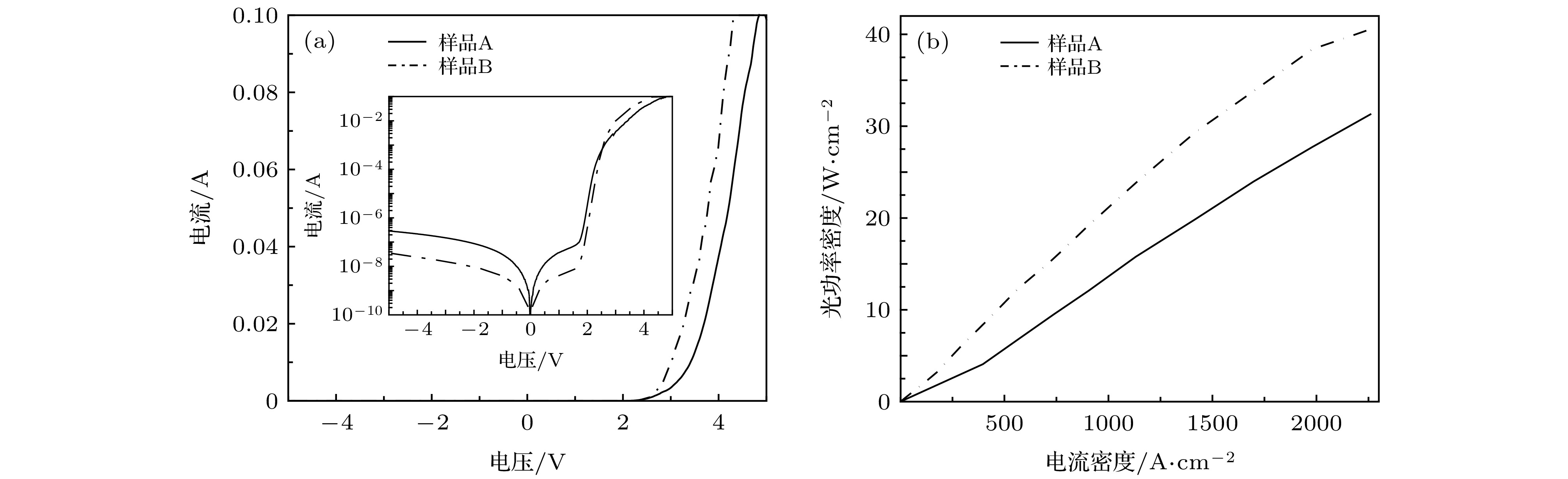 图 2 样品A和B 6 μm阵列的(a) I-V 特性和(b)光输出密度-电流密度特性
Figure2. (a) The I-V and (b) light output power density-current density characteristics of 6 μm arrays of samples A and B
发光孔径为6 μm的micro-LED阵列器件在20 mA下正向工作电压、–5 V时反向漏电流和2264 A/cm2时的光输出密度如表1所示.
| 样品 | 工作电压(20 mA)/V | 反向漏电流(–5 V)/A | 光输出密度(2264 A/cm–2)/W·cm–2 |
| A | 3.69 | 2.89 × 10⁻⁷ | 31.34 |
| B | 3.27 | 3.43 × 10⁻⁸ | 40.59 |
表16 μm micro-LED阵列光电性能参数
Table1.The photoelectric properties of 6 μm micro-LED array.
对比表1中样品A和B的各项光电特性参数可知: 与样品A相比, 样品B具有更好的光电性能, 具体表现为正向工作电压降低了11%, 反向漏电流降低了88%, 光输出密度增大了23%.
图3(a)为不同课题组台面刻蚀制备的micro-LED器件反向漏电流密度, 图3(b)为光输出密度, 可以看出, 离子注入制备的micro-LED阵列器件与台面刻蚀器件相比, 反向漏电流密度与光输出密度已经达到文献报道水平.
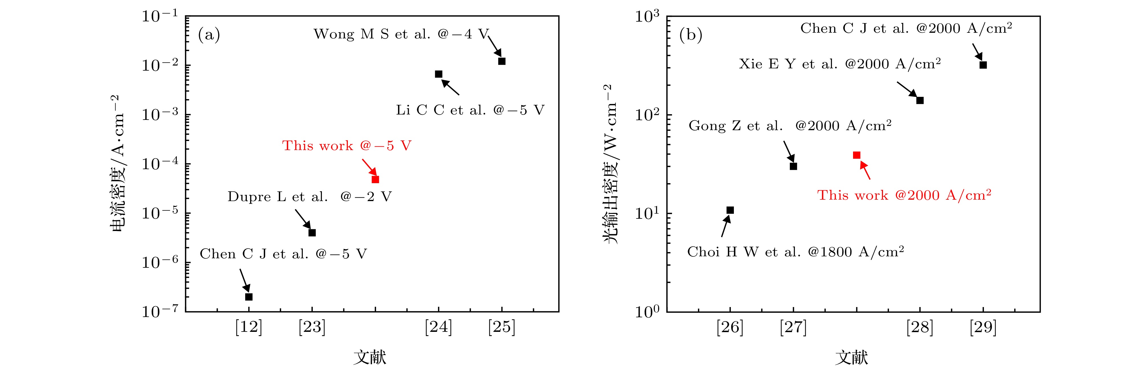 图 3 注入隔离micro-LED器件与台面刻蚀器件 (a)反向漏电流和(b)光输出密度比较
Figure3. Comparison of (a) reverse leakage current and (b) light output density between implanted isolated micro-LED devices and mesa etching devices.
进一步, 通过SRIM软件模拟了不同能量F离子注入条件下注入损伤与注入深度的关系[30], 如图4所示, 可以看出: 在50 和100 keV能量下分别进行F离子注入, 注入后损伤峰值分别出现在80 nm和182 nm处, 表明单次注入只对n-GaN部分区域实现了隔离, 在50 keV注入时, 对较浅区域起到隔离, 在100 keV注入时, 对较深区域实现了隔离; 50/100 keV能量F离子两次注入后, 损伤峰值出现合并, 这使得F注入隔离的整体损伤增大, 有利于提升器件的电学隔离效果. 由上述分析可知, 不同能量下离子注入损伤峰值存在明显差异, 且离子注入次数对损伤峰值也产生了显著影响, 因此根据SRIM模拟结果初步判断单次注入隔离不完全是导致样品A性能较差的主要原因.
 图 4 SRIM模拟F离子不同注入能量下产生的损伤与注入深度关系
Figure4. The relationship between damage and implantation depth of F ion with different implantation energies with SRIM simulation.
此外, 通过CTLM测试验证不同能量F离子对注入区域隔离效果的影响, 图4为CTLM测试原理图. 如图5所示, 内圆半径r0为70 μm, 且不随位置变化, 外圆半径为r1从小到大依次分别为80, 85, 90, 95, 105, 120 μm.
 图 5 CTLM测量原理图
Figure5. Schematic of CTLM test.
圆环内总电阻RT可表示为
令(1)式中

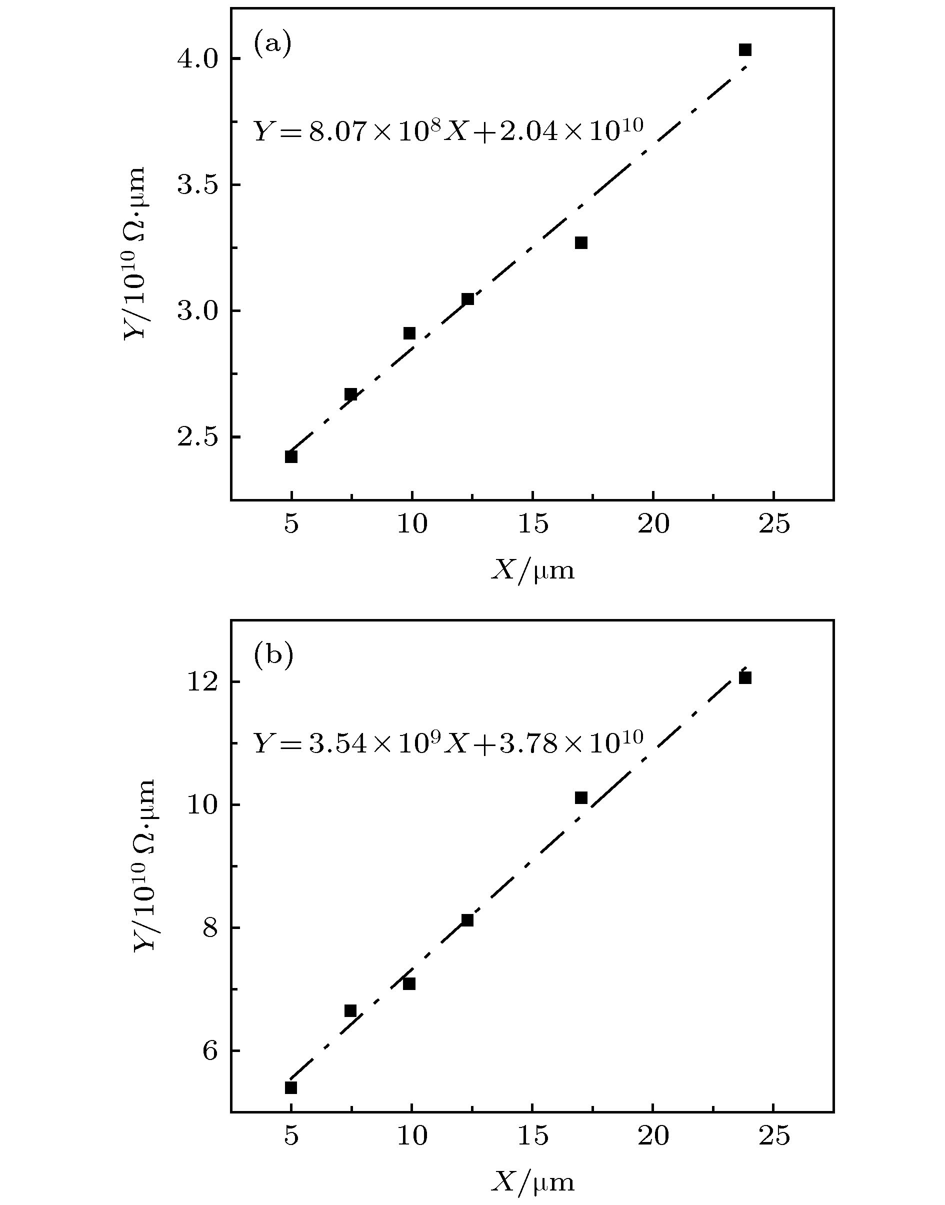 图 6 CTLM线性拟合曲线 (a) 50 keV能量注入; (b) 50/100 keV能量注入
Figure6. The CTLM linear fitting curve at (a) the implantation energy of 50 keV and (b) 50/100 keV.
结合CTLM测试及SRIM软件模拟结果可知: F离子注入n-GaN后, 注入区域方块电阻增大了约106—107倍; 单次注入对n-GaN隔离不完全, 导致注入区域方块电阻较小, 其方块电阻仅为两次注入区域的25%. 这说明了单次注入时样品A的隔离效果较差, 从而致使样品漏电流偏大、光输出密度偏小.
2
3.2.micro-LED发光孔径对其光电性能的影响
进一步测试样品B中6, 8, 10 μm不同发光孔径micro-LED阵列电学性能. I-V特性曲线如图7所示, 插图为样品半对数坐标下的反向I-V特性曲线. 从图7可以得出: 随着器件发光孔径的减小, micro-LED阵列正向工作电压从2.95 V增大到3.26 V, 串联电阻分别为14.3, 18.5, 22.2 Ω, 反向漏电流基本相同, 约为3.40 × 10⁻⁸ A, 且不随发光孔径的变化而出现明显差异, 说明micro-LED阵列反向漏电流只与离子注入隔离条件有关, 与发光孔径无关.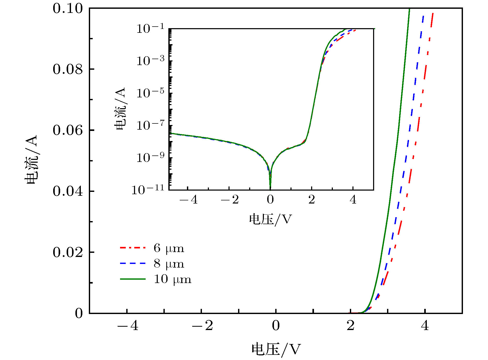 图 7 不同发光孔径阵列I-V特性曲线
Figure7. I-V characteristics of the different emission aperture arrays.
样品B不同发光孔径阵列在20 mA电流下实际发光情况如图8所示, 可以看出不同发光孔径下的micro-LED阵列都具有良好的隔离效果, 且发光效果较为均匀.
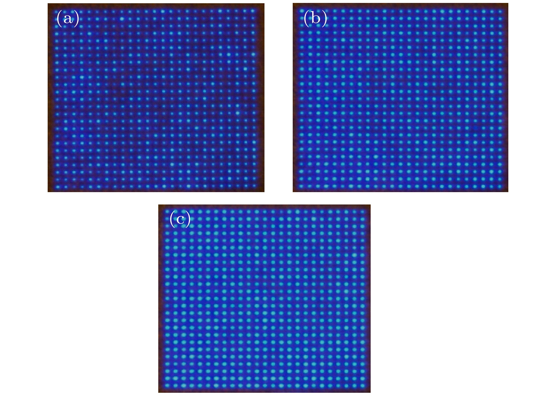 图 8 20 mA下 (a) 6 μm, (b) 8 μm, (c) 10 μm发光孔径阵列发光图像
Figure8. Light-emitting aperture arrays of (a) 6 μm, (b) 8 μm, and (c)10 μm at 20 mA.
表2为单颗发光孔径实际发光效果, 可以看出器件实际发光孔径小于设计的发光孔径, 减小了约0.47 μm, 主要原因是发光孔边缘区域产生了0.24 μm的注入损伤, 并且随发光孔径的减小, 有效发光面积比(S1/S2)从92%减小到85%; 此外, 10 μm台面刻蚀隔离器件存在约0.5—1.1 μm的侧壁损伤, S1/S2仅为(70±10)%[17]; 对比离子注入隔离器件与台面隔离器件实际发光效果可以得出, F离子注入后对边缘产生的损伤减小了0.26—0.86 μm, S1/S2提高了11%—31%, 表明F离子注入隔离可有效提高了micro-LED器件的有效发光面积.
| 器件尺寸/μm | 6 | 8 | 10 | 20[16] | 10[17] |
| 隔离方式 | 注入 | 台面刻蚀 | |||
| 实际发光区域 | |||||
| 实际发光面积S1/μm2 | 24.10 | 43.92 | 72.04 | 144 | 70 ± 10 |
| 器件面积 S2/μm2 | 28.26 | 50.24 | 78.50 | 400 | 100 |
| S1/S2/% | 85% | 87% | 92% | 36% | 70 ± 10 |
表2样品B单颗发光孔径实际发光情况
Table2.The actual emission condition of single light-emitting aperture in sample B.
