全文HTML
--> --> -->本文通过拉曼热测量技术准确表征了热压烧结法制备的铜/石墨复合物法兰封装的GaN场效应管在不同功率下的结温, 结合拉曼热测试与有限元热仿真结果的比对分析得到GaN器件的各层热阻, 并与由传统铜钼法兰封装的GaN器件进行对比. 结果发现由高热导率铜/石墨复合物法兰封装的GaN器件的整体热阻比由铜钼法兰封装的GaN电子器件的整体热阻低18.7%, 从器件层面证明使用铜/石墨法兰封装降低GaN器件热阻、提高热扩散能力的可行性. 同时, 本文也阐明应用拉曼热测量技术结合热仿真模型分析GaN电子器件各部分热阻的具体方法和独特优势.
 图 1 (a)被测GaN高电子迁移率场效应管器件结构以及拉曼热测量的示意图; (b)被测器件在50 ℃和300 ℃的拉曼特征峰: 包括GaN外延的E2(high)和A1(LO)峰, 以及SiC衬底的FTO峰
Figure1. (a) Schematic structure of the GaN-on-SiC HEMT under test in the Raman optothermal measurement; (b) Raman peaks of the GaN-on-SiC HEMT at 50 ℃ and 300 ℃, including the E2(high) and A1(LO) peaks of the GaN epitaxy and the FTO peak of the SiC substrate.
如图1(a)所示, 由于拉曼热测量技术中所使用的532 nm激光可以穿透同为宽禁带半导体的GaN和SiC, 而且拉曼光谱具有材料选择性, 因此被测器件GaN外延层和SiC衬底层的拉曼峰信息可被同时提取. 测量时激光透过数值孔径NA = 0.5的物镜, 聚焦在器件栅极脚下靠近漏极的一侧的AlGaN/GaN表面, 该区域电场强度最高, 为沟道内温度最高的区域. 拉曼热测量技术的原理是利用被测材料的拉曼特征峰具有温度依赖性, 这是晶格常数随着温度变化而改变, 而相应的声子振动模式的频率随之改变产生的. 对GaN和SiC来讲, 这种温度依赖性在室温以上是线性的, 即GaN和SiC的拉曼特征峰会随着温度的升高呈现线性的偏移[22], 通过偏移的波数值可以得到材料的温度升高值. 图1(b)为被测器件在50 ℃和300 ℃下的拉曼光谱, 包括GaN外延的E2(high)和A1(LO)峰, 以及SiC衬底的FTO峰, 可以看到GaN和SiC的特征峰随着温度升高发生红移.
为准确表征器件沟道和衬底上表层的温度, 首先对器件中GaN和SiC的温度系数进行校准. 在校准的过程中使用高精度温控台严格控制器件的温度, 从室温开始, 每升高25 ℃测量1次GaN和SiC的拉曼特征峰, 直到300 ℃. 图2(a)和图2(b)分别显示了被测器件GaN A1(LO)峰和SiC FTO峰位置随温度变化的关系, 通过线性拟合得到GaN A1(LO)峰的温度系数为–0.026 cm–1·K–1, SiC FTO峰的温度系数为–0.023 cm–1·K–1.
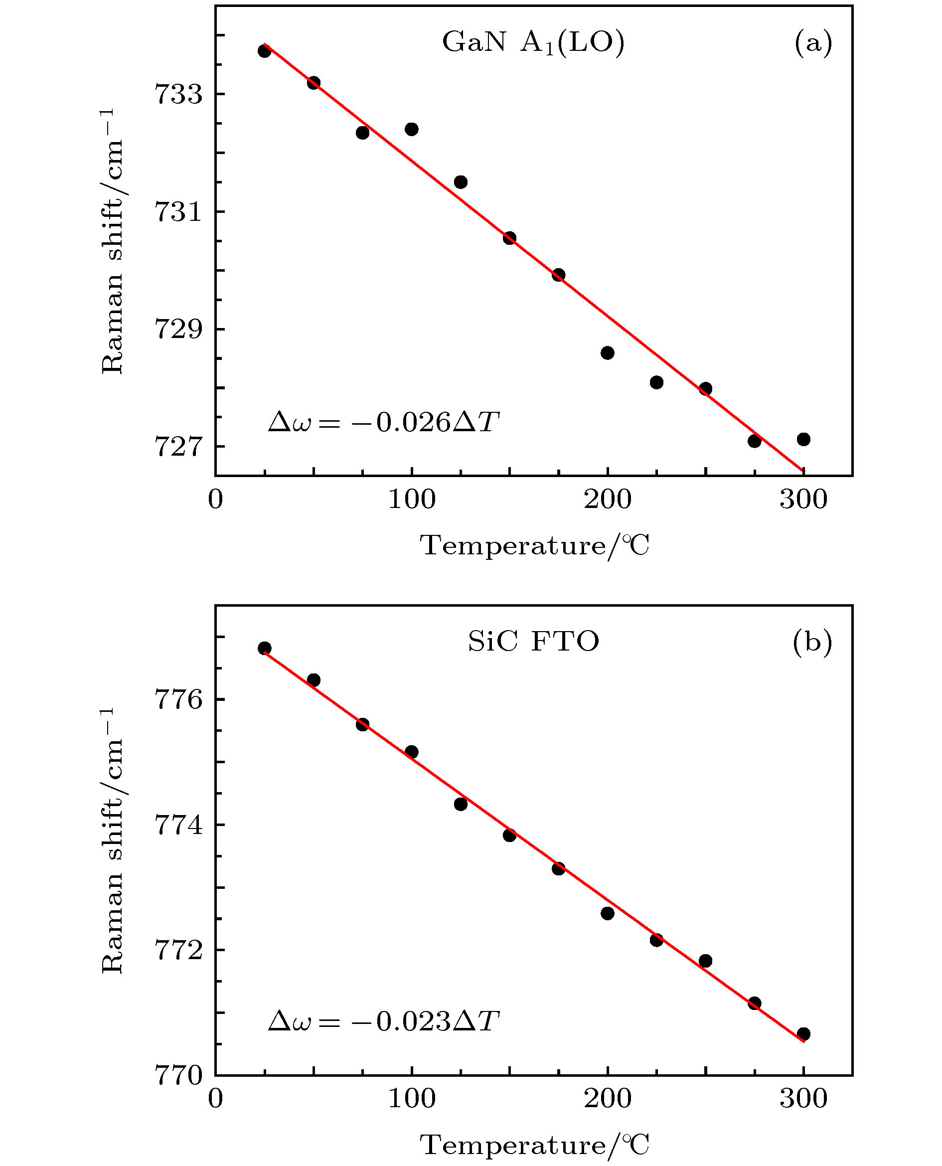 图 2 (a) GaN A1(LO)拉曼峰随温度的变化关系, 线性拟合得到的温度系数为–0.026 cm–1·K–1; (b) SiC FTO拉曼峰随温度的变化关系, 线性拟合得到的温度系数为–0.023 cm–1·K–1
Figure2. (a) Position of the GaN A1(LO) Raman peak as a function of temperature. The temperature coefficient from the linear fit is –0.026 cm–1·K–1; (b) position of the SiC FTO Raman peak as a function of temperature. The temperature coefficient from the linear fit is –0.023 cm–1·K–1.
得到校准的温度系数后, 测量器件在不同功率工作状态下GaN A1(LO)峰和SiC FTO峰的偏移. 由于器件的生热量随功率密度成正比例增加, GaN和SiC相应位置的温度也随功率密度的增加而升高, 造成的拉曼峰移随功率密度的线性关系的斜率称为GaN A1(LO)峰和SiC FTO峰的功率系数. 我们使用双通道直流电源分别给GaN器件的栅-源两极和漏-源两极之间施加电压, 用万用表测量漏极电流. 从器件关断状态(栅极负压)开始, 功率密度大约每增加0.3 W/mm需多次测量GaN A1(LO)峰和SiC FTO峰的峰位. 多次测量是为了尽可能的减少测量的不确定性, 提高测量准确度. 整个测量过程中将热电偶放置在电路板上靠近器件工作区域的位置, 测得的不同功率密度下的板温作为器件封装法兰背板的温度. 图3(a),(b)分别显示了被测器件GaN A1(LO)峰、SiC FTO峰随着功率密度升高的偏移, 通过线性拟合得到GaN A1 (LO)峰的功率系数为 –1.86 cm–1·mm/W, SiC FTO峰的功率系数为 –1.25 cm–1·mm/W.
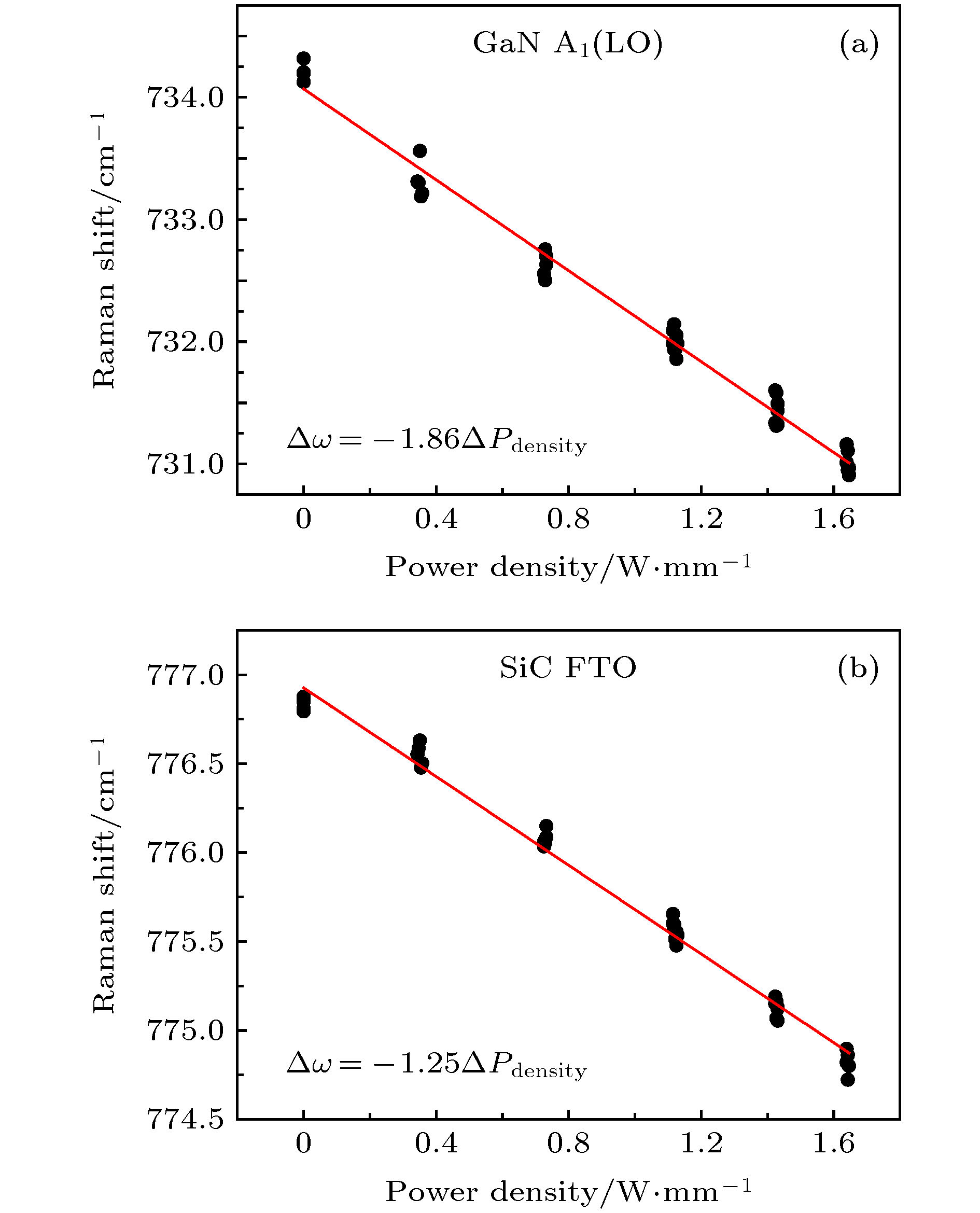 图 3 (a) GaN A1(LO)拉曼峰随器件功率密度的变化关系, 线性拟合得到的功率系数为–1.86 cm–1·mm/W; (b) SiC FTO拉曼峰随器件功率密度的变化关系, 线性拟合得到的功率系数为–1.25 cm–1·mm/W的功率系数
Figure3. (a) Position of the GaN A1(LO) Raman peak as a function of the device power density. The power density coefficient from the linear fit is –1.86 cm–1·mm/W; (b) position of the SiC FTO Raman peak as a function of the device power density. The power density coefficient from the linear fit is –1.25 cm–1·mm/W.
以特征峰的偏移作为中间变量即可得出不同功率密度下对应的器件中GaN外延的温度和衬底上表层的温度, 结合由热电偶测量的封装法兰的温度, 可以得到不同功率密度下对应的器件中沿纵向延伸不同深度处的温度. 需要强调的是, 拉曼光热实验中使用的激光波长(λ = 532 nm)和透镜的数值孔径 (NA = 0.5)决定了激光聚焦在GaN表面时景深为8—10 μm[18], 所以对透明的GaN来说拉曼探测的有效区域是整个GaN外延层厚度, 对SiC拉曼探测的有效区域是SiC衬底上表层(即界面处)的7—9 μm, 而通过拉曼峰移得到的温度是有效区域的平均温度. 实际上, 1—2 μm GaN外延层厚度的平均温度同器件结温非常接近, 详见第3节中的结果与讨论.
| GaN场效应管法兰封装材料 | 热导率/W·(m·K)–1 | GaN-SiC间热阻/mm·K·W–1 | 器件整体热阻/mm·K·W–1 |
| 铜/石墨 | 300 | 14.7 | 42.9 |
| 铜钼 | 167 | 14.4 | 52.8 |
表1两种铜基法兰封装GaN器件的热阻对比
Table1.Thermal resistance of GaN HEMT with different Cu-based flange materials.
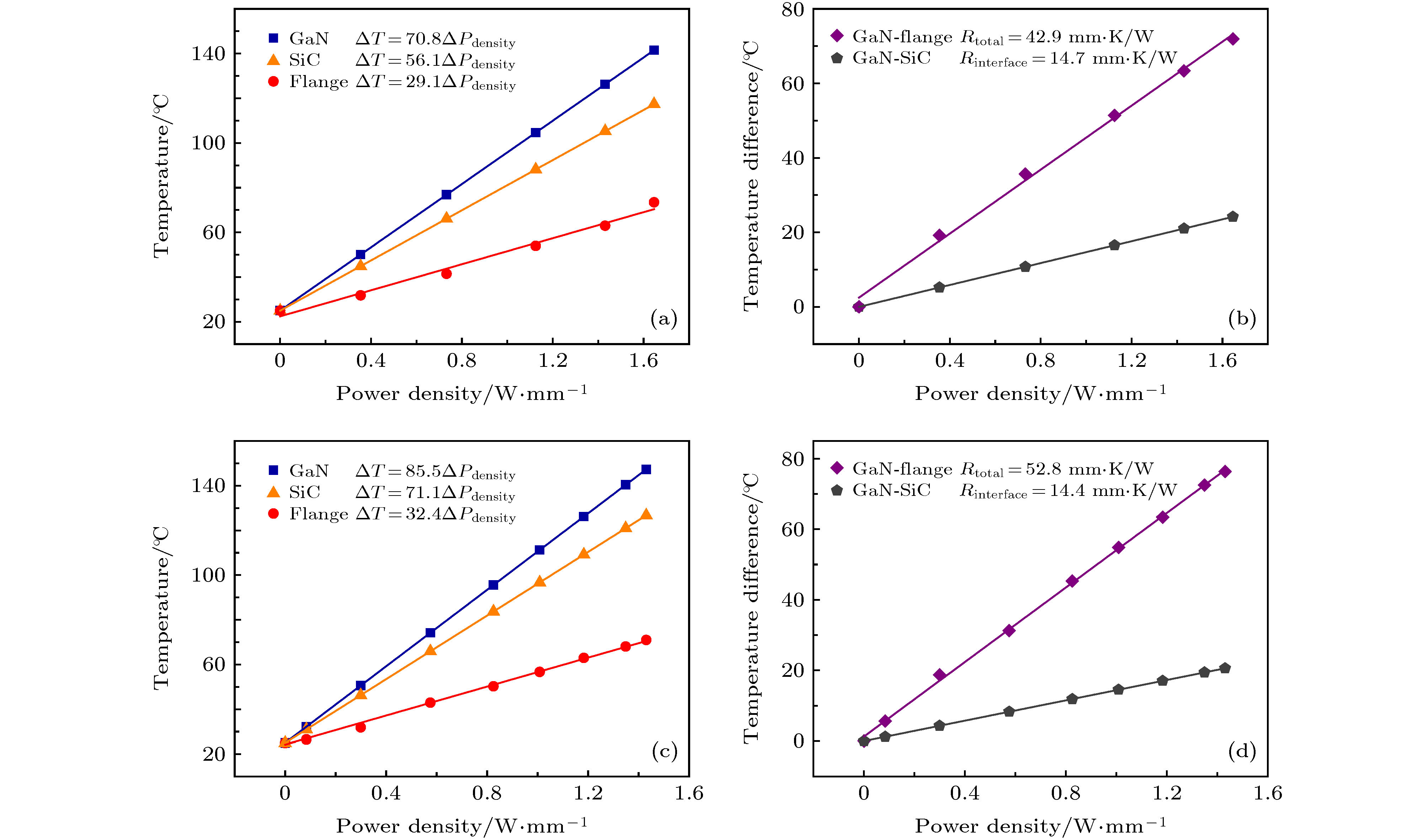 图 4 (a)铜/石墨法兰封装器件GaN层、SiC上表层和封装法兰的温度随功率密度的变化; (b)铜/石墨法兰封装器件GaN层和SiC上表层的温度差、GaN层和封装法兰之间的温度差随功率密度的变化; (c)铜钼法兰封装器件GaN层、SiC上表层和封装法兰的温度随功率密度的变化; (d)铜钼法兰封装器件GaN层和SiC上表层的温度差、GaN层和封装法兰之间的温度差随功率密度增加的变化
Figure4. (a) Measured temperature of GaN, SiC, and the Cu/graphite flange as a function of the device power density; (b) temperature differences between GaN and SiC, and between GaN and and the Cu/graphite flange as a function of the device power density; (c) measured temperature of GaN, SiC, and the CuMo flange as a function of the device power density; (b) temperature differences between GaN and SiC, and between GaN and and the CuMo flange as a function of the device power density.
为了更好地理解器件各层的热阻占比, 根据被测器件的实际几何尺寸以及实验测量的条件使用有限元热仿真模型模拟器件在对应功率密度下各层的温度, 其中使用的各层材料的几何参数和热学性质参数在表2中列出. GaN, SiC, AuSn等材料的热导率都是器件常用的文献值[23,24], 法兰封装材料的热导率是供应商提供的激光闪射导热仪的测量值. 热模拟中器件工作的功率密度作为热源的功率密度控制在0—1.7 W/mm范围内, 实验测得的法兰温度作为器件的边界温度. GaN与SiC之间的等效界面热阻, 包含20 nm厚成核层材料AlN的热阻以及GaN/AlN与AlN/SiC两个界面热阻, 被当作变量用于拟合GaN与SiC上表面温度的测量值. 当GaN-SiC等效界面热阻为50 m2·K/GW时, GaN与SiC温度的模拟值与测量结果匹配. 关于热仿真模型的更多细节可以参考本课题组的另一篇文章[25]. 值得注意的是, 这里用来拟合的GaN与SiC的温度为前文所述的拉曼探测有效区域的温度平均值, 而图5(a)和图5(b)分别显示铜/石墨法兰和铜钼法兰封装的GaN器件的结温(即GaN上表面峰值温度)和AlN/SiC界面温度的模拟值和实测值的对比, 会比GaN与SiC中探测有效区域的实测平均值略高(3%), 这个结果表明拉曼热测量技术的结果在GaN外延厚度不大(1 μm左右)的情况下足够接近GaN表面的峰值温度, 能较为准确和可靠地用于GaN器件结温和器件失效时间的评估.
| 材料 | 厚度/μm | 热导率/ W·(m·K) –1 |
| AlGaN/GaN | 1.2 | 160 × (T/300)–1.42[23] |
| AlN | 0.02 | 拟合提取出等效界面热阻约为50 m2·K/GW |
| SiC | 100 | 400 × (T/300)–1[23] |
| AuSn | 12 | 57[24] |
| 铜钼 | 1000 | 167[24] |
| 铜/石墨 | 1000 | 300 |
表2有限元热仿真分析中使用的各层材料的尺寸及热导率
Table2.Dimensions and thermal conductivity of each layer in the GaN-on-SiC HEMT used in the finite element device thermal simulation.
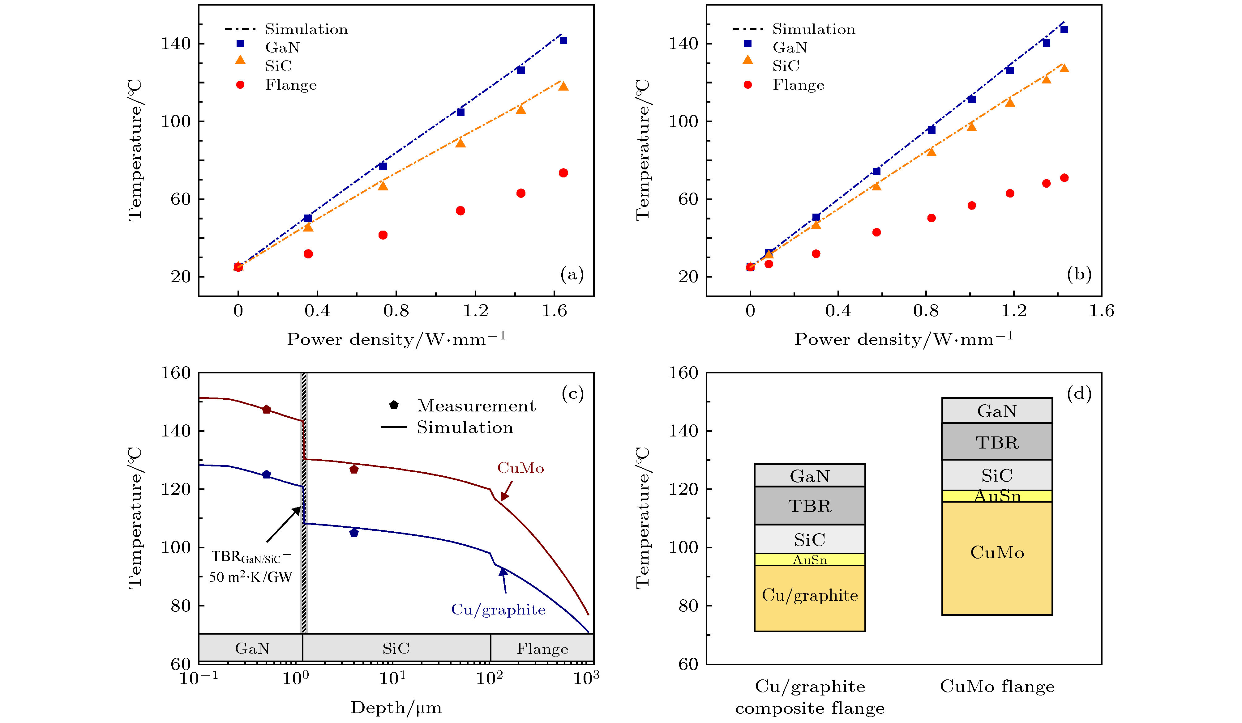 图 5 (a)铜/石墨法兰封装的GaN器件的GaN外延和SiC衬底上表层温度的模拟值(线)和实测值(点); (b)铜钼法兰GaN电子器件的结温和SiC衬底上表层温度的模拟值和实测值的对比; (c) 1.43 W/mm功率密度下铜/石墨法兰和铜钼法兰封装GaN器件在垂直器件表面方向上的温度分布; (d)铜/石墨法兰和铜钼法兰封装GaN器件各层材的热阻占比(其中TBR的材料为AlN)
Figure5. (a) Simulated (line) and measured (dot) junction temperatures of the Cu/graphite flanged device; (b) simulated (line) and measured (dot) junction temperatures of the CuMo flanged device; (c) depth wise temperature distribution of the Cu/graphite flanged device and the CuMo flanged device at the power density of 1.43 W/mm; (d) thermal resistance of each layer within the Cu/graphite flanged device and the CuMo flanged device (The material of TBR is AlN).
通过热仿真还可以得出被测GaN电子器件在垂直器件表面方向上的温度分布, 以及各层材料的热阻占比, 这样可以更直观地了解器件内部的热输运过程, 如图5(c)和图5(d)所示. 图5(c)为功率密度为1.43 W/mm情况下铜/石墨法兰器件和铜钼法兰器件的纵向温度分布, 图中的实线即为模拟值, 点则代表实际测量值, 拟合得到的GaN与SiC之间的等效界面热阻为50 m2·K/GW. 在功率密度均为1.43 W/mm的情况下, 铜/石墨法兰器件的模拟结温128.4 ℃比铜钼法兰器件的模拟结温151.3 ℃降低15.1 %; 两个器件唯一的差别就是封装材料不同, 表明器件导热性能的改良得益于封装材料热导率的提高. 如表2所示, 被测器件的铜/石墨复合法兰的热导率可达300 W/(m·K), 比铜/鉬法兰的热导率167 W/(m·K)高79.6 %. 此外, 从图4(a)和图4(c)的对比中可以发现, 铜/石墨法兰封装的器件中GaN外延、SiC衬底上表层、法兰背板的温度随功率密度升高的变化系数相比铜钼法兰封装器件的对应值分别降低17%, 21%, 11%, 表明在相同的功率密度下, 铜/石墨法兰器件的各层温度均低于相应的铜钼法兰器件的各层温度. 图5(d)直观地展示了1.43 W/mm功率密度下铜/石墨法兰器件和铜钼法兰器件的各层材料热阻占比. 对于整个器件来讲热阻占比最大的部分就是封装法兰, 其中铜/石墨法兰约占GaN电子器件整体热阻的40%, 铜钼法兰约占GaN电子器件整体热阻的53 %. 相较于铜钼法兰, 铜/石墨法兰的热阻占比降低了13%, 这个结果使器件的整体热阻降低18.7%. 本文所测的铜/石墨法兰的热导率为300 W/(m·K), 根据文献[16]的结果, 该热导率对应的石墨质量分数近似为50%. 如果进一步提高铜/石墨法兰的热导率, 比如石墨质量分数为40%的铜/石墨复合材料热导率可达378 W/(m·K)[16], 通过热仿真模拟的结果表明可以使器件的整体热阻降低19.8%. 通过调整铜/石墨复合材料中石墨的质量分数可以使法兰的热导率达到最佳. 这是因为虽然石墨本身的热导率高于铜的热导率, 但是随着石墨质量分数的增加, 铜与石墨的界面也会增加, 同时受热压烧结工艺的影响, 材料中的空隙也会增多, 这些因素均导致材料中的自由电子和声子散射的增多, 从而降低材料的热导率. 对图5(c)和图5(d)的分析还可以发现, 对于整个器件来说, 热阻占比较高的除了法兰之外, 还有界面热阻, 其占铜/石墨法兰器件整体热阻的22%和占铜钼法兰器件整体热阻的18%. 本文中拟合得到的GaN-on-SiC电子器件的界面热阻约为50 m2·K/GW, 与Riedel等[26]采用拉曼热成像技术的测量结果约47 m2·K/GW相近, 但是比本课题组采用瞬态热反射法测量的另一种工艺生长的SiC基GaN外延片的界面热阻约25 m2·K/GW高了1倍[27]. 通过有限元模拟发现, 如果器件的界面热阻降低到25 m2·K/GW, 则结温会进一步降低2.7%, 整体热阻会相应地降低5.6%. GaN晶片的界面热阻受外延生长工艺影响, 尤其是成核层内部或者界面附近的微观结构和缺陷会通过增加声子散射率、降低声子的平均自由程来阻碍热传递. 研究表明, 与常用的金属有机化学气相沉积相比, 热壁外延技术可以有效地降低GaN外延和SiC衬底之间的界面热阻[26]. 这是因为热壁外延技术生长的AlN成核层更趋向于单晶, 这导致了较少的缺陷、晶粒和晶界的声子散射, 因此成核层具有更高的热导率. 界面热阻的降低将会进一步提高器件的热扩散性能.
