全文HTML
--> --> -->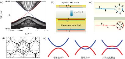 图 1 (a)拓扑绝缘体的能带结构示意图, 红色和蓝色分别表示自旋取向相反的两支边界态; (b) 二维拓扑绝缘体每个边界处存在两支相对运动的自旋流, 电荷流与电子自旋方向关联; (c) 量子自旋霍尔边缘非磁性杂质散射的两种可能路径, 顺时针(蓝色)或逆时针(红色)旋转的方式绕过此杂质, 会额外增加π或–π的相位, 使得自旋为1/2的电子路径相互抵消, 从而禁止背散射; (d) Haldane模型所描述的石墨烯晶格, 空白和黑点圆圈分别代表两类子晶格, 晶格内不同区域a和b分别产生交错的反向磁通, 整个晶格不存在净磁通; (e) BHZ模型中, 平庸绝缘体经过能带反转和自旋轨道耦合重新打开能隙, 实现拓扑非平庸绝缘体; 蓝色和红色表示能带的奇偶宇称性, 拓扑相变过程中伴随着能带宇称的交换((a)?(c)[1], (d)[3])
Figure1. (a) Energy spectrum of the topological insulator, there exist gapless edge states of spin-up (red) and spin-down (blue) connecting the conduction and valence band; (b) the one-dimensional (1D) conducting channels are spin polarized and spatially separated in a quantum spin Hall (QSH) insulator; (c) A QSH edge state can be scattered in two possible directions by a nonmagnetic impurity; clockwise (blue) and counterclockwise (red), accompanied with the spin rotated by π and –π, respectively, a quantum mechanical phase difference of 2π between the two paths leads to destructive interference, resulting in the suppression of backscattering; (d) the Haldane model of a graphene-like structure, the open and solid circles stand for two sublattices, within which different magnetic fluxes (equal but reversal direction) are assumed to passing through regions a and b; in each hexagonal cell, there is no net magnetic flux; (e) illustration of the band inversion mechanism in a BHZ model, blue and red colors represent bands with opposite parities. In the presence of SOC, the topologically trivial bands are in an inverted order and converted into a topological insulator. (a)?(c)[1], and (e)[3].
理论上先后提出过两个模型来预测和解释拓扑绝缘体. 其一是Kane和Mele基于Haldane的模型提出的[2]. Haldane模型假设在二维蜂巢状石墨烯晶格中存在与晶格周期、对称性都一致的反向交错垂直磁场, 使得两套子晶格所围成的特定区域(a和b)产生大小相等、方向相反的磁通Φ和–Φ (图1(d)), 就能够实现无需外磁场的整数量子霍尔效应[3]. 由于Haldane模型中没有长程相互作用, 且存在自发性连续对称性破缺, 因此无法在实验中严格实现. Kane-Mele模型认为, 固体内原子内禀的自旋轨道耦合效应(spin-orbital coupling, SOC)不破坏时间反演对称性, 可以充当反向交错磁场的角色. 进一步引入电子能带结构的拓扑不变量, 将具有能隙结构的绝缘体划分为普通绝缘体和拓扑非平庸绝缘体(即拓扑绝缘体)[2]. 但是石墨烯中的自旋轨道耦合效应太过微弱, 在倒空间K点打开的能隙过于微小(μeV量级), 实验上难以探测[4]. 另外一个模型是张首晟等[5]提出的Bernevig-Hughes-Zhang (BHZ)模型. 该理论用于描述窄带半导体中的拓扑相变: 先在半导体中引入能带反转, 再通过自旋轨道耦合重新打开能隙, 从而实现拓扑平庸到非平庸的转变(图1(e)).
利用上述的两个模型, 人们在理论上预言了许多潜在的二维拓扑绝缘体体系, 主要包括以下几类: 1)石墨烯及其衍生异质结; 2)量子阱体系; 3)二维层状单质或化合物; 4)五碲化合物以及Bi的卤化物等三维弱拓扑绝缘体; 5)类石墨烯的蜂窝状六角晶格体系; 6)1 T’结构的过渡金属硫族化合物; 7)一些有机材料; 8)狄拉克半金属等. 当前的文献报道中, 具备可观测的实验迹象并支持为二维拓扑绝缘体的体系只占很小部分. 表1列出了这些可能的候选材料[6].
| 研究体系 | 代表性材料 | 拓扑能隙 | 实验进展 |
| 石墨烯及相关异质结构 | Graphene | ~μeV | |
| Graphene/BiTeX | 70—80 meV | ||
| 5d吸附原子/Graphene | 0.2 eV | ||
| Graphene/Re/SiC(0001) | 0.1 eV | ||
| Ru/Graphene | 10 meV | ||
| In(Tl)/Graphene | ~7(20) meV | ||
| Bi2Se3/Graphene/Bi2Se3 | 30—40 meV | ||
| Sb2Te3/Graphene/Sb2Te3 | 1.5 meV | ||
| MoTe2/ Graphene/MoTe2 | 3.5 meV | ||
| 量子阱 | HgTe/CdTe | ~meV | 支持[7] |
| InAs/GaSb/AlSb | ~meV | 支持[9] | |
| GaN/InN/GaN | ~10 meV | ||
| GaAs/Ge/GaAs | ~15 meV | ||
| 二维层状单质或化物 | 单层Bi(111) | 0.2—0.6 eV | 支持[11] |
| 多层Bi(111)/Si(111) | 0.8 eV | 支持[14] | |
| Bi单晶 | — | 支持[13] | |
| Bi(110) | ~0.1 eV | 支持[52] | |
| 4层黑磷 | ~5 meV | ||
| 应力或电场下Sb(111) | — | ||
| 单层GaAs, BBi, AlBi | |||
| 三维弱拓扑结缘体 | ZrTe5/HfTe5 | ~0.1 eV | 支持[22-24] |
| Bi4I4 | — | 支持[27] | |
| Bi4Br4 | ~0.18 eV | ||
| Bi14Rh3I9 | ~0.2 eV | 支持[26] | |
| 类石墨烯六角蜂窝晶格 | Silene(硅烯) | 2 meV | |
| Germanene(锗烯) | 23.9 meV | ||
| Stanene(锡烯) | ~0.1 eV | 支持[35], [37] | |
| Bismuthene(铋烯) | 0.67 eV | 支持[38] | |
| 1 T’相过渡金属硫族化合物 | 1 T’-WTe2 | ~0.1 eV | 支持[40-42] |
| 1 T’-WSe2 | ~0.1 eV | 支持[47-48] | |
| 有机材料 | Ni3(C18H12N6)2 | 16—23 meV | |
| Ni3C12S12 | 22.7和9.5 meV | ||
| Pb(C6H5)3/Bi(C6H5)3 | 43和8.6 meV | ||
| δ-石墨炔 | 0.59 meV | ||
| 石墨化-C6N6 | 5.50和8.27 meV | ||
| 官能团修饰材料 | –F, –Cl, –Br, –I, –OH修饰的锡烯/锗烯 | ~0.3 eV | |
| –H, –F, –Cl, –Br, –I, –CH3修饰的单层Bi(111)/Sb(111)/双层Pb | ~0.3—1 eV | ||
| -Cl修饰的GaBi | 0.65 eV | ||
| 狄拉克半金属薄膜 | Na3Bi | 层厚依赖~0.3 eV | 支持[57] |
| Cd3As2 | 层厚依赖~0.11 eV | 支持[55] | |
| 过渡金属氧化物 | 双层LaAuO3 | 0.15 eV | |
| 重金属元素化合物 | TlBi | 56 meV | |
| TlAs | 0.131 eV | ||
| TlSb | 0.268 eV |
表1理论预言的二维拓扑绝缘体候选材料, 以及当前的实验进展, 只有少量体系获得了实验观测的证据支持(大部分结果摘自参考文献[6]及其该文所引文献)
Table1.Theoretical predictions of two-dimensional topological insulator candidates and the current experimental progress, only a few systems are supported by experimental observation evidence (most of the results are extracted from Ref. [6] and the references cited in this paper).
实验上第一次观测到量子自旋霍尔效应是在HgTe/CdTe量子阱中[7], 该体系具有BHZ模型所描述的能带反转诱导的拓扑相变. 其中: CdTe是平庸的绝缘体, 当HgTe的厚度小于临界值(dc < 6.3 nm)时, 受到CdTe的近邻作用, 表现出拓扑平庸的绝缘体特性. 而HgTe厚度大于dc时会发生能带反转, 具有奇宇称的Hg的s轨道(Γ6)上升到具有偶宇称的Te的p轨道(Γ8)之上, 从平庸绝缘体变成二维拓扑绝缘体(如图2(a)). 实验上通过输运测量观察到量子化的自旋霍尔电导, 且不随样品的横向尺度而变化, 说明该量子化的霍尔电导来源于边界(图2(b)), 从而证实HgTe/CdTe量子阱是量子自旋霍尔绝缘体. 然而, HgTe/CdTe量子阱的制备非常困难, 热稳定性也差. 该体系的拓扑能隙不到10 meV, 大大小于室温下的热展宽(~26 meV), 其拓扑效应只能在非常低的温度下才能观测到, 难以走向应用. 另外, 由于该体系的异质结构型, HgTe被埋在CdTe之下, 难以利用表面敏感的探测手段直接观测其边界态. 2008年, Zhang等[8]预言了一种基于传统Ⅲ-Ⅴ族半导体材料的AlSb/InAs/GaSb/AlSb量子阱结构, 结构上的非对称性使得反演对称性被破缺, InAs中能量最低的电子态处于GaSb中能量最高的空穴态之下, 从而形成反带. 该体系的量子自旋霍尔效应很快被Du研究组[9]所证实.
 图 2 (a) 理论计算HgTe和CdTe能带结构, 超过临界厚度时HgTe将发生能带反转[5]; (b) 通过输运实验, 测量HgTe/CdTe量子阱的量子化霍尔电导平台, Ⅰ表示样品厚度小于临界值, 处于平庸绝缘体状态, Ⅱ、Ⅲ、Ⅳ表示样品厚度大于临界值, 体系进入量子自旋霍尔态, 量子化电导与样品的横向尺寸(L和W)无关[7]
Figure2. (a) Bulk energy bands of HgTe and CdTe near the Γ point. Bellows are schematic illustration for the subbands of CdTe/HgTe quantum well in the normal (d < dc) and inverted regime (d > dc), respectively[5]. (b) experimentally measured longitudinal resistance of various normal (d = 5.5 nm) (Ⅰ) and inverted (d = 7.3 nm) (Ⅱ, Ⅲ, and Ⅳ) devices as a function of gate voltage. Quantized resistance plateaus are observed due to the perfectly conducting edge states of a QSH insulator, which is regardless of the lateral dimensions (L and W)[7].
在新型二维原子晶体材料的制备和性能调控获得广泛探索之后, 实验上对于二维拓扑绝缘体的研究成为热点, 一些表面敏感的探测工具如扫描隧道显微镜(scanning tunneling microscopy, STM), 角分辨光电子能谱(angle-resolved photoemission spectroscopy, ARPES)等被广泛应用于二维拓扑物态的研究之中. ARPES可以直接探测到材料的能带结构, 用于表征二维拓扑绝缘体的体能隙. 但是边界在样品中只占很小的比例, 边界态的贡献很小, 无法直接得到拓扑边界态的信息. 而STM可以直接将针尖定位在二维材料边界, 局域地探测到边界态的信号. 与此同时, 还能得到体能隙的信息, 观测结果直接明确; 并与ARPES、输运等测量结果对照, 互为补充, 是研究拓扑边界态不可或缺的探测手段. 近年来, STM技术在研究二维拓扑绝缘体方面取得了一系列成果, 下面着重介绍几类受实验迹象所支持的典型二维拓扑体系.
2.1.铋
目前实验上获得证据支持的二维拓扑绝缘体, 大多数隶属于BHZ模式, 其核心要素是体系中元素具有较强的自旋轨道耦合作用. 作为第Ⅴ族的重元素, 铋(Bi)具有非常强的自旋轨道耦合强度(~1 eV), 而且可以以二维的形式稳定存在. 因此, 其二维薄膜形式下的拓扑特性被广泛关注.实验上研究最多的是Bi(111)取向的表面, 其晶体结构一般以翘曲石墨烯结构存在, 包含两套具有不同原子高度的子晶格, 从而自发形成双原子层结构(bilayer, BL). 理论计算预言单个BL层厚的Bi(111)薄膜为量子自旋霍尔绝缘体[10]. Jia研究组[11]成功地在三维拓扑绝缘体Bi2Te3表面制备出单层Bi(111)薄膜, 并通过STM测量观察到: 电子态密度在靠近薄膜台阶处相较于体内有显著增强, 且实空间分布不随能量变化(图3(a)). 该边界态的空间穿透深度为2 nm左右, 空间延展范围远大于原子晶格间距, 由此排除了悬挂键等边界局域因素的影响. 图3(b)的密度泛函理论(density functional theory, DFT)计算给出了倒空间不同点对应的实空间边界态分布, 表明单层Bi(111)薄膜确实存在边界电子态, 且具有2 nm的穿透深度. 通过对比STS, ARPES和DFT计算的电子结构(图3(c)), 进一步证实了该一维边界态局域在体能带的能隙(橙色虚线)之中, 表明STM观察到的边界态具有拓扑性质. 由于最顶层的Bi(111)薄膜与衬底间存在电荷转移, 体能隙位于费米能级之上, 且STS在体内本应为能隙的能量区间出现了非零的电导. 因此, 体能隙的大小由ARPES测量和DFT计算所定出(~0.1 eV), 并受面内应力作用所调控. 然而, 实验并未直接探测到Bi(111)薄膜的体能隙. 考虑到Bi2Te3衬底本身也是拓扑绝缘体, 两者可能产生较强的耦合作用, 进而影响到Bi(111)薄膜的边缘态性质, 所以STM测量的边缘态来源存在一定争议. 随后, Kim等[12]在计算上考虑了衬底和Bi(111)薄膜之间的强耦合, 导致Bi(111)的体能隙关闭, 而引入一个相对较小的杂化能隙. 但是衬底耦合不会破坏单层Bi(111)薄膜的拓扑边界态, 并在三维拓扑绝缘体Bi2Te2Se衬底上得到验证.
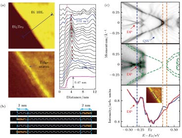 图 3 (a) Bi2Te3表面1 BL层厚Bi(111)薄膜台阶边缘的形貌图和实空间电导成像, 存在不随能量变化的一维边界态; (b) 理论计算显示台阶处的能带结构存在拓扑边界态, 穿透深度~2 nm; (c) 1 BL层厚Bi(111)薄膜的电子能带结构, 从上到下分别为DFT计算结果、ARPES和STS谱数据, 显示出边界电子态密度增强发生于体能隙内, DP表示狄拉克点, QW表示量子阱态; 橙色虚线代表最顶层1 BL Bi(111)薄膜的体态能隙[11]
Figure3. (a) STM image and STS map of 1 BL Bi/Bi2Te3 island, showing apparent 1D edge states near the step. The red dashed lines indicate the location of step edges. The red dots mark the peak position of the edge states. (b) real-space charge density distribution of the edge states by calculations. (c) the electronic structures of 1 BL Bi/Bi2Te3. Calculated density of bands (up), ARPES spectrum (middle), STS of the step edge and the inner terrace (bottom, blue and red, respectively) are aligned by the Dirac point “DP” the blue dashed line, “QW” marks the quantum well states. Adapted from [11].
从晶体结构来看, 双原子层的Bi原子呈翘曲结构排列, 不同原子层和衬底之间的间距有所不同, 会形成两种类型的边界结构, 如图4(a)的A, B所示, 两种边界与衬底之间存在不同强度的耦合. Yazdani研究组[13]率先在单晶Bi表面观测到这两种边界在电子态分布上的区别(图4(b), (c)). 尽管两类边界都是锯齿形(zigzag)结构, 但A边的Bi原子距离衬底较远, 可以和衬底发生脱耦合, 能够保留一维拓扑边界态. 而B边与衬底的相互作用较强, Bi(111)的电子态将产生强烈的杂化效应, 遏制了边界态的出现.
 图 4 (a) 翘曲型的双原子层Bi(111)结构, 夹角为120°的两条边界自然地形成A和B边两种边界, Bi原子与衬底存在不同距离高度; (b) 对比Bi(111)两种边界以及远离边界处的扫描隧道谱(STS, 可以看成实空间局域电子态密度随着能量的分布); (c) 183 meV能量下电子态密度的空间分布图, 显示A边存在拓扑边界态, 而B边则不存在; (d) 沿着A边所做的STS线谱(沿着边界等间距取得一系列STS谱, 并组合成二维分布的谱图), 表明台阶边缘处存在一维边界态(红色高亮部分), 体内也能观测到电子态散射所形成的驻波; (e) 傅里叶变换结果显示, 动量空间存在q1和q2两类散射通道; (f) 理论计算显示, 自旋选择散射允许q1散射通道存在, 禁止q*(背散射通道)存在[13]
Figure4. (a) Schematics of 1 BL Bi atomic structure with two types of edges. (b) point spectroscopy at the two different types of edge A (red) and B (blue) and on the surface away from the edges (grey). (c) STS maps for a hexagonal pit-like defect at +183 meV. High conductance (red) is observed at every other edge (type A). (d) spectroscopy along the type A step edge. 1D singularity exactly at the edge is observed by approaching the step edge, spectra far from the edges show the 2D surface electronic properties of Bi(111). (e) 1D Fourier transform of the quasi-particle interference (QPI) within the edge channel. Two QPI branches (q1 and q2) are identified, with the q1 branch corresponding to the 1D edge state and q2 branch from the projection of 2D surface states. (f) dispersion calculation of the scattering within the 1D edge mode. Considering the spin properties, only scattering between the states of similar spin (q1) is allowed, while the backscattering channel (q*) is strongly suppressed. Adapted from [13].
我们知道: 电子以波的形式在空间传递, 且容易被材料表面的杂质或边界所散射, 最终电子波将相互叠加而形成一定的驻波态. 这些由等能面之间散射所形成的驻波能在实空间中稳定存在, 通过STM探测分析出动量空间的能带色散关系, 进而获得材料费米面的信息. 为了证实观测到的一维边界态具有拓扑属性, 根据STM测量实空间和能量尺度上电子态密度的驻波分布(图4(d)), 通过傅里叶变换的方式, 得到准粒子的能量-动量(E–k)关系, 如图4(e)所示. 主要存在两种散射通道: q1和q2, 其中q1来源于一维边界态相同自旋方向电子态之间的散射, q2是体电子态在边界上的投影. 结合理论计算的进一步分析表明, A边的一维边界态展示出二维拓扑绝缘体所特有的散射特点: 相同自旋的散射被允许, 相反自旋的散射由于时间反演对称保护而被禁止(如图4(f)). 这种选择性的散射可以用拓扑态的自旋与动量锁定来解释, 因此强烈支持Bi(111)是二维拓扑绝缘体. 类似的结果在Si(111)衬底上生长的Bi(111)薄膜中也被报道[14].
无论是Bi/Bi2Te3, Bi单晶还是Bi/Si(111)薄膜, 都需要考虑衬底的作用, 且测量的都是单个Bi双原子层. 那么衬底到底在决定Bi(111)的拓扑性质方面扮演着什么角色呢? 厚层Bi(111)薄膜是否仍然是二维拓扑绝缘体呢? Wang研究组[15]发现: Bi(111)薄膜因较强的SOC作用而出现分裂的量子化表面态(Landau能级), 且其自旋极化的能谷电子态几乎不随薄膜层厚的增加而改变. 近年来, 有理论计算表明: 当Bi(111)的厚度超过8个原子双层时将发生拓扑相变, 从二维拓扑绝缘体变成拓扑平庸态[16]. 最近, 我们精确控制Bi(111)薄膜层数, 利用STM测量发现: 即使厚度超过9 BL时, 仍然存在一维传播的拓扑边界态[17]. 通过选取超导性的NbSe2作为衬底, 发现Bi(111)边界上存在两种能量较低的结构, 分别为1 × 1 (zigzag)和2 × 1重构两种边界. 利用衬底的超导近邻效应, 证明两类边界均不存在磁有序, 并不破坏时间反演对称性, 这为观测拓扑边界态提供了基础(如图5(a)). 实验发现, 这两种边界均存在一维的拓扑边界态, 但表现出不相同的能量范围和空间扩展(图5(b)). 对于不同层厚的Bi(111)薄膜, 无论边界是否发生重构, 台阶处STS谱的范霍夫奇点 能量始终低于对应台面的值, 且均随着层厚的增加 向低能量方向移动, 直至趋近体态Bi单晶(图5(c)). 这些结果表明: Bi(111)薄膜的厚度和特定边界构型, 对其拓扑边界态只能产生定量上的调制, 而不能改变其拓扑特性. 另外, 测量结果验证了理论所预言的双层Bi(111)也是二维拓扑绝缘体, 表明Bi(111)的层间耦合作用在决定其拓扑性质方面具有重要作用[18].
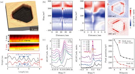 图 5 (a) Bi(111)薄膜呈现长短两种类型的台阶边界, 交替排布并形成六边形, 高分辨STM图显示边界分别为zigzag(黑)和2 × 1重构(红)两种结构, 表现为不同的面内晶格常数; (b) 1 × 1和2 × 1两种边界处各自的拓扑边界态, 展现出不同的空间和能量分布, 右边为不同能量下态密度的实空间分布, 显示两种结构均展现一维特性的边界态; (c) 随着层厚的增加(4—10 BL), 无论是台面上(左)还是边界处(中), 范霍夫奇点的峰位均向低能量方向移动, 直到趋近于Bi单晶(右). 这表明1 BL层厚Bi(111)的二维拓扑特性并不受衬底薄膜的厚度而影响[17]
Figure5. (a) Two types of edge structures, zigzag and 2 × 1 reconstructed edge, coexist alternately at the boundaries of 1 BL Bi islands. Displayed from the atomically resolved STM images and line profiles, the two edge show different in-plane lattice constants. (b) 2 D plot of tunneling spectra across the zigzag and 2 × 1 edge, respectively, exhibiting remarkably different energy and spatial distributions. Right images are the spectroscopic mapping, showing alternating appearance of edge states for the 2 × 1 edge at 100 mV and zigzag edge at 200 mV. (c) a series of STS spectra recorded on the Bi terrace (left) and at the step edge (middle) from 4 to 10 BL. Spectra are shifted vertically. Right is the energy evolution for the topological edge states with various thicknesses of underlying Bi substrate. Adapted from [17].
近年来, 理论和实验均表明: d维的Bi(111)体系极有可能是属于高阶拓扑绝缘体, 不仅存在(d–1)维边界态, 也存在(d–2)维的边界态. 不同于常规的二维拓扑绝缘体中一维的无能隙边界态, 高阶拓扑绝缘体中的边界态将打开能隙, 并在能隙中存在稳定的角态或棱态[19]. STM测量也观察到Bi(111)台阶边处的一维边界态保持C3旋转对称性, 即棱态, 并利用约瑟夫森干涉仪证明了它们对电子输运的拓扑贡献[20].
2
2.2.三维弱拓扑绝缘体
二维拓扑绝缘体可叠加形成三维弱拓扑绝缘体. 对于三维拓扑绝缘体的四个拓扑指数(v0, v1, v2, v3), 如果v0不等于0, 即为所谓的强拓扑绝缘体, 其所有表面均具有无能隙的狄拉克表面态; 如果v0 = 0, 而v1, v2, v3不全为零, 则称为弱拓扑绝缘体, 只有特定取向的面才具有狄拉克表面态[1,3]. 由于大多数的拓扑绝缘体都是层状材料, 当三维弱拓扑绝缘体层间耦合足够弱, 可以将其看作是一系列二维拓扑绝缘体堆垛得到, 因此也能在晶体的台阶处产生量子自旋霍尔态. 而强拓扑绝缘体的台阶处, 拓扑边界态将与体材料的拓扑表面态杂化, 失去原有的拓扑边界态性质.2014年, Fang等在理论上预言了五碲化物XTe5(X = Zr/Hf)在薄膜形式下是二维拓扑绝缘体, 其三维形式则处在强拓扑和弱拓扑绝缘体的相变点上. 不同于常规的BHZ模型, XTe5的能带反转并非源自于自旋轨道耦合效应, 而是因为晶体具有特定的非中心对称空间群(Pmmn或D132h), 形成0.4 eV的直接能隙和0.1 eV的间接能隙. XTe5的拓扑特性受到层间耦合强度的调制, 只需要将层间距增加0.25 ?(3.4%), 就能使其从强拓扑绝缘体变为弱拓扑绝缘体[21]. 很快, Pan研究组和Li研究组分别独立利用STM表征了ZrTe5单晶样品, 发现了100 meV[22]和80 meV[23]的体态能隙, 其能隙区域的电子态密度完全为零(图6(a), (b)). 靠近台阶边界处, 体能隙区域出现非零的态密度, 表明边界态的出现. 该边界态有两个特点: 一是边界态密度在体能隙能量范围内强度基本不变(如图6(c)), 二是边界态密度的空间衰减长度约为1.5 nm (图6(d)). 这两者均与第一性原理计算的结果相一致(图6(d), (e)), 支持其边界态的拓扑起源. 能量依赖的ARPES测量表明该材料层间耦合很弱, 满足前文提及的产生二维拓扑边界态条件. HfTe5的STM研究给出了基本一致的结果: 单晶是三维弱拓扑绝缘体, 台阶边缘存在位于体能隙内的一维拓扑边界态[24]. 然而, 同时期ZrTe5单晶的STM实验测量给出了相反的结果[25], 该实验没有看到表面能隙, 认为三维的ZrTe5是强拓扑绝缘体. 考虑到ZrTe5处于强拓扑和弱拓扑的相变点附近, 其拓扑性质很容易受到层间间距的调制, 微小的压力都可能导致强-弱拓扑绝缘态的转变, 并引起表面态的变化. 不同研究组制备出的单晶样品有所差别, 这可能是实验上观测到不一致结果的原因.
 图 6 (a) ZrTe5晶体台阶附近的STS谱, 台面上具有~100 meV的体能隙, 台阶边缘处(红色曲线)态密度不为零, 表明存在位于体能隙内的边界态[22]; (b) 理论计算的态密度分布, 插图为顶层台阶处态密度, 和实验结果一致[22]; (c) 不同能量下ZrTe5台阶附近态密度的实空间分布图, 显示空间均匀分布的一维边界态[23]; (d) 理论计算的ZrTe5能带结构, 显示出狄拉克型色散的拓扑边界态[22]; (e) 体能隙中态密度积分强度逐渐远离台阶的变化, 给出边界态的衰减长度约为1.5 nm[22], 插图为第一性原理的计算结果((c)[23])
Figure6. (a) STS spectra along a line perpendicular to a monolayer step edge of ZrTe5. Red curves are tunneling spectra measured near the step edge. The inset shows the STM image of the step[22]. (b) calculated density of states of the top monolayer. The inset shows the edge states along the chain direction[22]. (c) STM topography of the step and the corresponding STS mapping taken at various bias voltages[23]. (d) calculated band dispersions of the edge states of the monolayer along the chain direction[22]. (e) normalized conductance integral within the gap plotted as a function of the distance from the edge. The exponential fitting gives a decay length ξ~1.5 nm[22]. Inset plots the calculated result with ξ~1.6 nm ((c) is adapted from [23]).
除了五碲化物, 一些由铋和卤族元素形成的化合物在理论上也被预言是拓扑绝缘体. 例如: Bi14Rh3I9采取[(Bi4Rh)3I]2+和[Bi2I8]2–两种原子层交错堆垛的方式, 如图7(a)所示. 其中原子层[(Bi4Rh)3I]2+是二维拓扑绝缘体, 原子层[Bi2I8]2–是拓扑平庸绝缘体, 插层于二维拓扑绝缘体之间, 这使得[(Bi4Rh)3I]2+层之间的耦合作用被大大削弱, 满 足了三维弱拓扑绝缘体的基本条件. 在[(Bi4Rh)3I]2+层中, 以Rh原子为中心的Bi原子立方体形成蜂窝状排布(图7(b)). STM测量结果[26]表明: 在作为缓冲层的[Bi2I8]2–原子层中, 只有~400 meV的平庸绝缘体能隙. 在[(Bi4Rh)3I]2+层的台阶边缘则出现了边界态. 边界态不受边界构型的影响, 并且在–450 — –200 meV的能量范围内保持空间位置不变. STM同时测量到了~200 meV的体能隙, 而且边界态确实发生于体能隙的能量区域(图7(c)), 这表明该边界态具有拓扑起源.
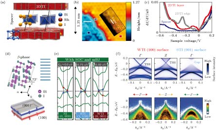 图 7 (a) Bi14Rh3I9晶体结构示意图, 分为平庸绝缘体的[Bi2I8]2-插层和二维拓扑绝缘体[(Bi4Rh)3I]2+层, 垂直方向上晶格间距为1.25 nm; (b) 不同原子层和台阶边缘的结构, 蓝色为[Bi2I8]2–层, 黄色为蜂窝状结构的[(Bi4Rh)3I]2+表面; (c) 不同区域电导谱比较, 在二维拓扑绝缘体[(Bi4Rh)3I]2+台阶边, 体能隙之内出现了明显的态密度增强, 费米能级附近的电导下降来自于库仑阻塞效应; (d) β-Bi4I4的准一维晶体结构, 沿着a和c方向都很容易解离, 分别得到(001)和(100)表面; (e) 理论计算的β-Bi4I4能带结构图, 不考虑SOC时为大能隙的平庸绝缘体, 考虑SOC则显示存在能带反转和拓扑表面态, 红色和蓝色圆圈表示能带宇称的奇偶性; (f) (100)侧表面观察到准一维狄拉克拓扑表面态, 而(001)顶表面没有拓扑表面态, 证明β-Bi4I4是三维弱拓扑绝缘体((a)?(c)[26], (d)—(f)[27])
Figure7. (a) Atomic model of Bi14Rh3I9, containing the normal insulating [Bi2I8]2– layer and 2 D TI [(Bi4Rh)3I]2+ layer. The distance along the vertical direction is 1.25 nm. (b) STM image with the step edge of [(Bi4Rh)3I]2+ layer (yellow). Inset is the zoomed-in view of the step edge in a honeycomb lattice. (c) STS spectra taken at the positions marked in (b) by the corresponding colors. The linearly vanishing STS intensity around EF is attributed to a two-dimensional Coulomb gap. (d) Crystal structure of the β-Bi4I4, which is easily cleaved along a and c directions, resulting in the (001) and (100) surfaces. (e) Band inversions of the β-phase with inclusion of SOC. The red and blue circles label respectively the even and odd parities for the bulk bands at the M and L points. NI stands for normal insulator. (f) The topological surface states at the side surface (100) for the weak TI and the strong TI phase along distinct high-symmetry lines. Up, calculations; down, ARPES data. (a)?(c) are adapted from [26], and (d)?(f) are from [27].
Bi4X4(X = Br, I, F)是另一类可能实现二维拓扑特性的大能隙材料, 并在最近的ARPES测量中获得验证[27]. 如图7(d), β-Bi4I4是准一维晶体结构, 在(001)和(100)两个方向都很容易解离, 同时暴露出表面和侧面, 成为研究弱拓扑绝缘体的绝佳体系. 实验上探测到在(100)表面存在准一维的狄拉克型拓扑表面态, 而在(001)面则不存在拓扑表面态(图7(f)), 证明了其三维弱拓扑特性. 由于β-Bi4I4也是以范德瓦尔斯层间耦合的方式堆垛的, 由三维晶体解离出的薄膜很可能具备二维拓扑特性. 类似地, 理论计算也表明Bi4F4和单层Bi4Br4分别具有0.69 eV[28]和0.18 eV[29]的体能隙, 布里渊区Γ点附近的能带发生反转, 表现为二维拓扑绝缘体(图7(e)).
2
2.3.类石墨烯六角蜂窝晶格体系
前文提到, 石墨烯中自旋轨道耦合很弱, 打开的能隙非常小, 不便于实验观测. 考虑到元素的自旋轨道耦合强度与其原子序数的四次方成正比, 根据Kane-Mele模型, 与碳同族但更重的元素(如硅、锗、锡、铅等), 若能形成类石墨烯的蜂窝状晶格, 极有可能具有实验可观测的体能隙以及拓扑特性. 理论计算确实表明硅烯, 锗烯和锡烯分别在狄拉克点处打开2 meV, 23.9 meV[30]和~100 meV[31]大小的能隙. 在无衬底的自由漂浮情况下, 除了石墨烯以外, 硅烯、锗烯和锡烯等由于较弱的π键, 一般形成翘曲结构(类似于Bi(111)薄膜). 这种结构的π键可以与σ键杂化, 从而降低体系自由能, 使结构稳定[32]. 因此, 非石墨烯的烯类无法以sp2形式在自然界存在, 实验上想要合成此类材料, 需要利用衬底的耦合作用使其稳定. 在ZrB2, Ir(111), Ag(111)等衬底上可以成功合成硅烯[33]. 但由于能隙较小, 加上来自于衬底的强烈影响, 实验上尚未观测到其拓扑特性. 锗烯也可以在各种金属衬底如Pt(111), Cu(111), Ag(111)以及非金属的Sb(111)和MoS2[34]上制备. 衬底上合成的锗烯会丧失其无质量狄拉克费米子特性, 这可能来源于衬底所引起的应力、电学掺杂以及轨道杂化等效应. Jia研究组最早利用分子束外延生长技术在Bi2Te3衬底上制备了单层锡烯薄膜, 并通过同步辐射光源和表面电子掺杂方法证实了其大能隙特性[35]. 实验上也在InSb衬底上合成了翘曲结构的锡烯[36], 但是并未观测到二维拓扑特性.通过适当的衬底耦合作用, Zhao研究组在Cu(111)表面制备出无翘曲的纯平锡烯. 在这种情况下, 锡烯的面内原子晶格会被拉伸, 进入二维拓扑绝缘态. 如图8(a)的STM原子分辨所示[37]. Cu(111)衬底饱和掉锡烯的面外取向的pz轨道, 留下面内取向的pxy轨道, 从而稳定其纯平的表面结构. ARPES数据显示该体系在布里渊区的Γ点具有相当大(~0.3 eV)的体能隙(图8(b)), 这与理论上考虑了Cu(111)衬底的耦合作用后所得出的预期一致. 同时, 通过STM也观测到表面台阶处的电子态密度增强, 能量区间在–1.2 eV至 — –1.45 eV之间, 与ARPES测量到的能隙相一致(如图8(c)). 尽管Cu(111)是金属衬底, 可能对表面锡烯产生不利影响, 类似于Ag(111)衬底上的硅烯. 但是理论计算依然给出边界态存在狄拉克型色散, 说明锡烯的边界态并未被衬底的金属态所破坏, 二维拓扑特性依然存在. 值得一提的是, 虽然是蜂窝状结构, 但是纯平锡烯面内晶格被拉伸, 其拓扑非平庸能隙不再位于K点, 而是转移到了Γ点. 二维拓扑特性并非由Kane-Mele模式在K点打开能隙所导致, 而是在Γ点附近s-pxy能带反转引入的, 亦即BHZ模式.
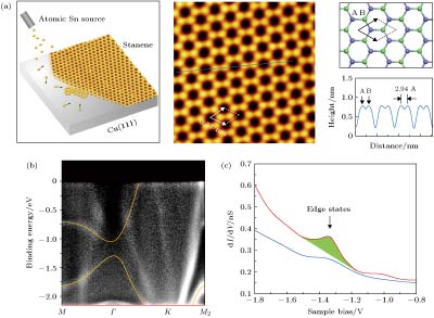 图 8 (a) Cu(111)表面外延生长的锡烯, 原子分辨显示结构为蜂窝状排布, 且相邻锡原子(A和B)的表观高度相同, 表明两套子晶格没有发生翘曲; (b) ARPES表明布里渊区Γ点打开0.3 eV的体能隙(黄色), 其余能带均来自于Cu(111)衬底; (c)锡烯台面上和台阶处的STS谱对比, 电子态密度的谱权重在偏压为–1.2 V到–1.45 V之间发生显著增加(绿色阴影部分), 正是来源自边界态, 且位于体能隙之内[37]
Figure8. (a) Sample growth set-up and the high-resolution STM image of the stanene film. The profile shows that the adjacent Sn atoms are identical in apparent height, confirming the atomic model of the honeycomb stanene. (b) ARPES spectra of 0.9 ML stanene along the M-Γ-K-M2 directions. The orange lines outline the energy bands which are contributed mainly by orbitals of Sn. Other branches come from the Cu(111) substrate. (e) STS spectra taken at the edge and center of the stanene flakes. The green shadowed regions between –1.2 V and –1.45 V high light the differences of enhanced spectral weight, which is attributed to the edge states. Adapted from [37].
另外, Bi虽然不属于第四族元素, 但是其强自旋轨道耦合使得其在二维拓扑绝缘体研究领域备受关注. 之前提到的翘曲型Bi膜在(111)取向的表面具有拓扑特性. 当其翘曲结构变成平整结构时, 便成为所谓的铋烯. 通过衬底调制, Reis等[38]在碳化硅(SiC)衬底上制备出铋烯, 形成单层Bi的蜂窝状二维晶格(图9(a), (b)). 研究发现, 碳化硅衬底可以与Bi膜之间形成共价键, 从而调制出较大的拓扑能隙, 同时, 衬底也起到稳定铋烯结构的作用. 与具有相同结构的石墨烯不同, 铋烯的费米面由Bi的σ轨道占据, 较大的拓扑能隙来自σ轨道的局域自旋轨道耦合, 同时原子序数较大的铋原子也使得拓扑能隙进一步增大, 实现拓扑能隙高达0.8 eV的量子自旋霍尔效应. 如图9(c)所示, STM观测到一维边界上的量子拓扑态, 与ARPES测量得到价带顶处的能级劈裂, 以及理论计算结果高度符合. 尤其值得注意的是, 碳化硅是绝缘衬底, 使得拓扑边界态与体态相分离, 为实现室温自旋电子学创造了极佳的工作环境. 但是, 由于该体系的铋烯岛尺寸仅有几十个纳米, 还不能满足其量子自旋霍尔效应的测量条件.
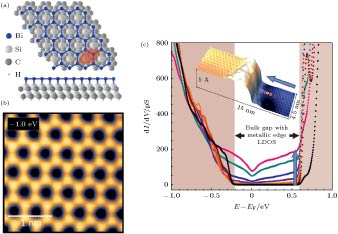 图 9 (a) 碳化硅(SiC)表面的单层铋烯的晶格结构示意图; (b) STM原子分辨显示无翘曲的Bi表面原子呈蜂窝状排布; (c) 单层台阶附近的STS分布, 靠近边界时, 铋烯由绝缘态变为金属态, 体能隙内出现显著的拓扑边界态, 插图为靠近边界时采集一系列STS谱的不同位置[38]
Figure9. (a) Sketch of a bismuthene layer placed on the SiC(0001) substrate. (b) close-up STM images for the occupied states, confirming the formation of Bi honeycombs. (c) STS spectra at different distances to the edge. A large gap of ~0.8 eV is observed in bulk bismuthine (black curve). Upon approaching the edge, additional signal of increasing strength emerges that fills the entire gap. Inset is the measurement locations near the boundary. Adapted from [38].
2
2.4.1 T’相过渡金属硫族化合物
由较重的过渡族金属(W/Mo)和硫族元素(S/Se/Te)形成的硫族化物(transition metal dichalcogenides, TMDC), 是以范德瓦尔斯力层间耦合堆叠的层状材料, 其二维结构是三明治型的三角晶系. 该体系中过渡金属元素具有较强的自旋轨道耦合, 也可能具有二维拓扑特性. 理论预言: TMDC材料具有比较大的平庸能隙, 不利于导带和价带的能带交叠, 无法通过能带反转的方式发展出拓扑特性. 但是, 在薄层状态下, TMDC的1 T结构不稳定, 会通过结构翘曲形变为1 T’结构(如图10(a)), 这种结构允许硫族元素的p轨道和过渡族金属元素的d轨道发生交叠和能带反转(如图10(b)), 自旋轨道耦合将打开100 meV左右的能隙, 诱导产生拓扑特性, 表现出BHZ模式的二维拓扑特性[39]. 不同TMDC薄膜本身所具有的体能隙不一样, 所产生的反转能带大小也不尽相同, 如图10(c)所示.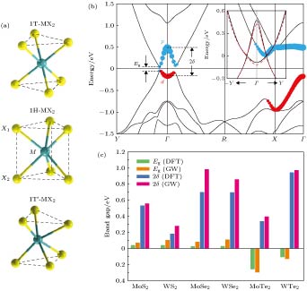 图 10 (a) TMDC的三种晶体结构; (b) 1 T’-MoS2通过p-d能带反转和自旋轨道耦合打开能隙, Eg为材料的本征半导体能隙大小, 2δ表示能带反转的能隙大小, 插图为有(红色)和无(黑色)自旋轨道耦合时的能带结构; (c) 利用不同计算方法分别得到TMDC薄膜的本征能隙和反带所打开能隙的大小对比[39]
Figure10. (a) Atomistic structures of three types of monolayer MX2, M stands for (W, Mo) and X stands for (Te, Se, S). (b) band structure of 1 T’-MoS2. The conduction and valence bands display a camelback shape near Γ, suggestive of band inversion with a large inverted gap of ~0.6 eV. Eg is the fundamental gap and 2δ is the inverted gap. Inset compares the band structures with (red) and without (black) SOC. (c) comparison for the fundamental and inverted gaps of all six 1 T’-MX2 materials by different calculation methods. Adapted from [39].
实验上目前研究的较多的TMDC材料是WTe2和WSe2. 其中, 在1 T’-WTe2的单晶样品表面台阶处(图11(a),(b))[40]和单层薄膜边界[41,42]都存在一维的导电通道, 即边界态. 单晶WTe2是第二类外尔半金属, 其结构以范德瓦尔斯方式进行层间堆叠, 所以最表层的WTe2受到单晶衬底的影响较为微弱, 可以看作一层自由的二维拓扑绝缘体. 第一性原理计算对比了自由漂浮的单层WTe2和考虑衬底时WTe2纳米带的能带结构, 表明衬底的存在并不会对表层的边界态产生实质的影响. STM结果发现边界态沿台阶方向等距离均匀分布(穿透深度约2 nm), 具备一维特性. 而且, 该边界态不受边界构型影响, 具有鲁棒性(图11(b)), 这表明该边界态不是由边界电势或重构等因素导致的[40]. 另外, 体相WTe2在加压[43]或化学掺杂[44]的情况下会进入超导态, 体相的超导和表层的拓扑特性耦合可能驱使WTe2单晶进入拓扑超导状态[45], 单层的WTe2薄膜甚至在表面电子掺杂时也能出现超导[46], 颇具研究价值. 结合ARPES探测到~40 meV的体能隙(图11(c)), 该边界态确实发生在体能隙内, 证实了WTe2薄膜的二维拓扑特性.
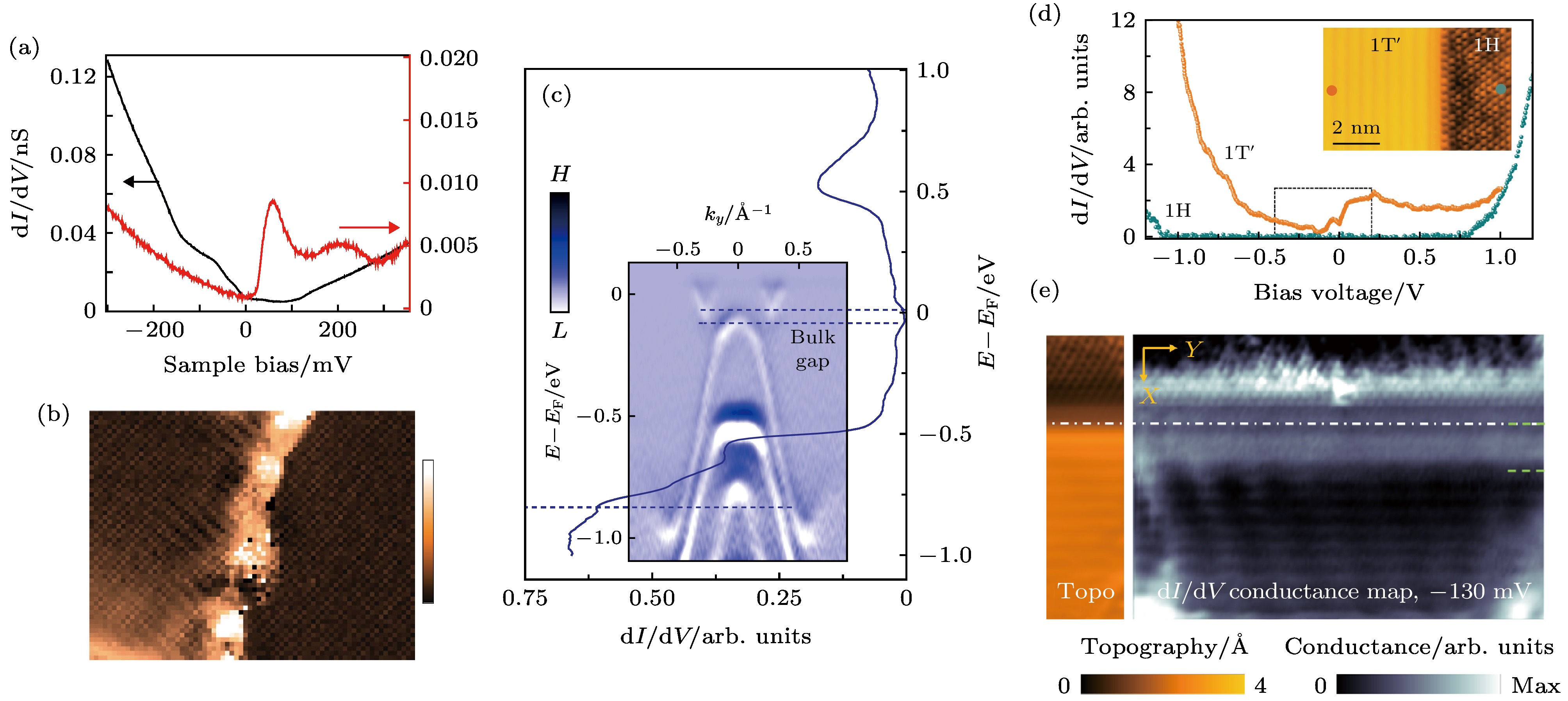 图 11 (a) 在1 T’-WTe2单晶表面台面上(黑)和台阶处(红)的STS谱; (b) 台阶附近单能量电子态密度分布图, 显示存在一维的边界态, 且不随台阶不规则形状而变化; (c) 1 T’-WTe2薄膜的STS谱和ARPES测量沿着Γ-Y方向的能带结构对照, 证实其平均能隙大小为(56 ± 14) meV. 样品表面进行了K原子掺杂处理, 以使得两者的化学势保持一致; (d) 1 H相和1 T’相WSe2的STS谱对比, 前者是大能隙的普通绝缘体, 后者是二维拓扑绝缘体, 插图为原子高分辨相; (e) 不同相之间畴界的形貌(左)和能隙内特定能量下能态密度的空间分布(右), 畴界处形成一维的拓扑边界态((a)和(b)[40], (c)[41], (d)和(e)[48])
Figure11. (a) Typical tunneling spectra measured at the step edge (red curve) and on the inner terrace (black curve). (b) spectroscopic mapping of the 1 T’-WTe2 step at selected voltages, showing the spatial distribution residing at an irregular shaped step edge. (c) STS spectrum and ARPES data acquired in the bulk of monolayer 1 T’-WTe2, which are aligned in energy in a K-doped sample for proper comparison. (d) STS spectra obtained in the 1 T’ (orange) and 1 H (blue) regions of single-layer WSe2. The former one is a normal insulator with a large band gap, the latter is a 2D TI. Inset shows an STM image of coexisting 1 T’ and 1 H regions with a well-ordered interface. (e) STM topography and experimental STS map (–130 meV) of the 1 T’-1 H interface. Dashed line shows interface location. High contrast are the edge states along the crystalline phase boundaries. (a)?(b) are adapted from[40], (c) are from [41] and (c)?(d) are from [48].
对于WSe2薄膜, 通过分子束外延方式所制备的结构与衬底温度紧密相关. 石墨烯衬底上制备的单层WSe2薄膜, 在高温(> 400 ℃)生长条件下是1 H结构, 呈现为常规的半导体性质, 是平庸的绝缘相. 但在低温下转变为1 T’相, 其体能隙约为130 meV, 表现出拓扑非平庸的特性(图11(d)). 此时, 1 T’相的边缘处出现明显的拓扑边界态[47]. 即使在1 T’和1 H相混合的样品中, 在1 T’相和1 H相的晶界处, 也能通过STM观察到一维的边界态. 如图11(e), 随着针尖靠近晶界, 体能隙能量范围内的电子态密度逐渐增强, 同样支持该边界态的拓扑起源[48].
通过结构调制拓扑相变的一个典型例子是Bi(110)薄膜. 对于在Si, NbSe2或高定向热解石墨(highly oriented pyrolytic graphite, HOPG)衬底上外延生长的Bi薄膜, 当薄膜层厚小于4层时, Bi(111)发生结构相变, (110)取向的形成能更低, 结构更稳定(图12(a)). 根据Bi原子双层是否发生翘曲行为, Bi(110)相分为黑磷结构(BP)和畸变型黑磷结构(distorted black phosphorus, DBP). 理论计算显示: Bi原子翘曲的程度会显著改变Bi(110)的拓扑特性[52], 过大的翘曲会使其由拓扑态变为平庸绝缘体(图12(b)). 实验上也通过STM观测到: 在HOPG衬底上制备的2层和4层Bi(110)薄膜, 翘曲程度较小, 存在较大的体能隙和位于体能隙内的拓扑边界态(图12(c)), 从而表明Bi(110)薄膜也是二维拓扑绝缘体.
 图 12 (a) Bi(110)的翘曲双原子层结构, h代表翘曲的程度; (b) Bi(110)的拓扑性质和能隙大小随翘曲高度变化的关系图, 当h < 0.1 ?时成为非平庸拓扑绝缘体; (c) 2层和4层的Bi(110)台阶边处STS谱有所增强, 显示拓扑边界态的存在[52]
Figure12. (a) Crystal structure of 2D Bi(110) thin films. Buckling is defined in terms of the height difference (h) between two atoms of the same monolayer. (b) buckling-dependent energy gap at Dirac point of Bi(110) film. When h is smaller than 0.1?, the Bi(110) film is converted into a 2D TI with topological nontrivial properties. (c) STS spectra taken from the edge to inside of the terrace of 2 ML (up) and 4 ML (down) Bi(110) film. The gap size determined far away from the edges is indicated by dash lines on both STS maps. Adapted from [52].
此外, 量子尺寸效应和电场也能有效地调控二维拓扑绝缘体的电学和拓扑性质. 例如: 理论计算预言, 三维拓扑狄拉克半金属(Na3Bi和Cd3As2)在薄膜中将打开能隙. 随着薄膜层厚的降低, 发生拓扑相变, 从二维拓扑绝缘体变为平庸的绝缘体(图13(a))[53,54]. 我们最近的工作证实了可以通过控制Na3Bi薄膜的层厚来调控其拓扑和物态性质[55]. 如图13(c)所示, 当Na3Bi薄膜层数大于四层时表现为半金属态. 而薄于四层时, Na3Bi薄膜会打开能隙, 从拓扑半金属转变为绝缘体. 其中, Na和Bi的轨道存在s-pxy能带反转, Bi元素的自旋轨道耦合效应使得费米能级附近打开能隙(图13(b)). 实验测得3层和4层的能隙分别为72和65 meV, 远高于室温能量尺度(26 meV). 高分辨的准粒子干涉结果也证实了Na3Bi薄膜存在狄拉克锥形的能带色散结构, 并在小于4层时打开了能隙. 与此同时, 在Na3Bi薄膜的边界观察到了不依赖于边界结构的一维边缘态, 其空间扩展长度约为4 nm (图13(d)). 结合第一性原理计算, 证实该边缘态具有拓扑属性, 在小于四层时是二维拓扑绝缘体.
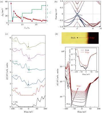 图 13 (a) 早期理论计算的Na3Bi的能隙(红点蓝线)和陈数(绿色曲线)随薄膜层厚的变化情况; (b) 最近理论计算三层Na3Bi薄膜的能带结构, 存在s-pxy能带反转, 自旋轨道耦合效应使得费米能级附近打开能隙, 成为二维拓扑绝缘体; (c) 实验上不同层厚Na3Bi薄膜的STS谱, 从体相的无能隙三维狄拉克半金属转变为有能隙的二维拓扑绝缘体; (d) 三层Na3Bi薄膜的STM形貌(上), 靠近台阶边缘时一系列STS谱的演化(下); 能隙内态密度逐渐增强, 表明存在拓扑边缘态, 插图为台面和台阶处STS谱采用对数坐标下的对比((a)[54], (b)?(d)[55])
Figure13. (a) Confinement-induced bulk gap (red dots) and the spin Chern number (green dashed line) as a function of the film thickness, showing a periodic modulation between normal insulator and 2D TI. (b) calculated band structure of 3 ML Na3Bi with SOC, showing a s-p band inversion. The including of SOC opens a Dirac gap near Γ point. (c) series of STS spectra recorded on Na3Bi terraces with different thicknesses (3-8 ML), showing a phase transition from a bulk gapless Dirac semimetal to a gapped insulator. All spectra are shifted vertically for clarity. (d) STS spectra in a logarithmic scale recorded near the step edge. Inset is a direct comparison for the bulk spectra with one at the edge. (a) is adapted from [54], and others are from [55].
外场调控同样能对Na3Bi薄膜的二维拓扑特性产生深刻的影响. 在垂直于薄膜的电场诱导下, Stark效应使得其体能隙逐渐减小至关闭. 进一步增强电场将再次打开带隙, 诱导子能带发生反转, 成为二维拓扑绝缘体(图14(a))[56]. 最近的实验结果也验证了此类拓扑相变. Collins等[57]利用表面蒸镀碱金属原子和STM针尖操纵的方式, 在Na3Bi薄膜表面产生可变电场. 他们通过控制碱金属原子的覆盖度或针尖与样品表面的距离, 成功地对样品施加不同强度的电场(图14(b)). 系统性的数据表明, 随着电场强度的增大, Na3Bi的能隙先关闭然后重新打开(图14(c)), 产生了电场诱导的拓扑相变(图14(d)).
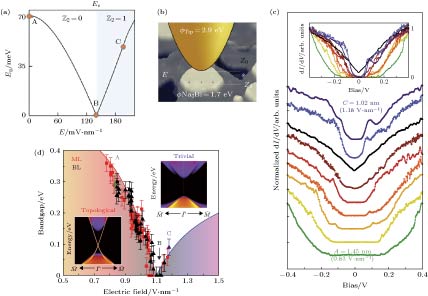 图 14 (a)理论计算Na3Bi薄膜在电场作用下将发生拓扑相变, 由平庸绝缘体转变为拓扑绝缘体; (b) 实验上, 实空间中Na3Bi小岛和STM针尖测量示意图; (c) 随着针尖逐渐靠近样品表面, 产生逐渐增强的电场, Na3Bi薄膜的能隙关闭后再次打开, 插图为不同电场下STS谱归一化原始数据, 在拓扑相变点变为金属态; (d) 单层和双层Na3Bi薄膜的能隙随外加电场增大的演化图, 在临界电场EC = 0.1 V/?附近发生拓扑相变, 插图分别为理论计算拓扑非平庸的边界态和普通绝缘体的能带结构((a)[56], (b)?(d)[57])
Figure14. (a) Variation of energy gap in a Na3Bi thin film as a function of the vertical field with the gap closing and reopening process. A field-induced topological phase transition is predicted between Z2 = 0 phase and Z2 = 1 phase. (b) Schematic of a STM tip at distance above the surface of Na3Bi, with the difference in work function ψTip-ψNa3 Bi generating a localized electric field. (c) Normalized STS spectra taken on 2 ML Na3Bi at different tip-sample separations, where A, B and C correspond to tip heights (electric fields) of 1.45 nm (0.83 V·nm–1), 1.07 nm (1.12 V·nm–1) and 1.02 nm (1.18 V·nm–1), respectively. Inset shows the spectra without offset, highlighting the clear non-zero conductance in a metallic state. (d) Bandgap extracted from STS spectra as a function of electric field for 1 ML (red squares) and 2 ML (black triangles) Na3Bi. Topological phase transition occurs at the critical electric field of EC = 0.1 V/?. Insets represent the calculated edge state band structures for the topological nontrivial and trivial states. (a) is adapted from [56], and others are from [57].
在实际的电子器件中, 通过外场调控拓扑相变可以等效为操纵器件的开关, 量子自旋霍尔绝缘体与平庸绝缘体分别对应于开和关的状态. 傅亮等人基于TMDC材料设计出一种利用垂直电场操纵的拓扑场效应晶体管(topological field-effect transistor, TFET), 该器件主要利用了TMDC材料的拓扑能隙在外加垂直电场下具有可调性(见图15)的特性[39]. 理论计算表明, 当电场超过临界值(EC = 0.1 V/?)后, TMDC中原有的拓扑能隙被关闭, 并相应产生平庸能隙. 这一转变意味着边界导电通道从有到无, 对应了电子器件的开和关两种逻辑状态. 由此可见, 通过探索新型的结构稳定, 并有可观体带隙的二维拓扑绝缘体, 既可以研究其丰富的奇异物态和量子特性, 如高温量子自旋霍尔输运, 拓扑边界态的相互耦合以及拓扑量子相变等, 也有利于推动对二维材料的多自由度调控(掺杂、应变、电场和磁光等), 构建适于产业化的逻辑开关器件, 引导未来新一代超低能耗电子器件的应用.
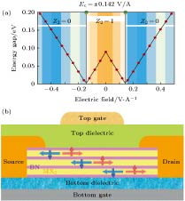 图 15 (a) 垂直方向电场对1 T’-MoS2拓扑特性的调控, 当垂直电场的强度超过~0.14 V/?时, 体系进入拓扑平庸状态, 与此同时, 能隙也经历了先闭合再打开的过程; (b) TFET概念图, 晶体管上下使用大能隙的六角氮化硼(h-BN)作为门电极, 中间夹层的TMDC薄膜也用h-BN彼此绝缘, 外加电场可以调控器件边界导电通道的开关[39]
Figure15. (a) Topological phase diagram of 1 T’-MoS2 as a function of vertical electric field. The critical field strength is ~0.14 V/?, marked by two green dots. (b) schematic of topological field effect transistor. The central component is a van der Waals heterostructure of alternating monolayer 1 T’-MX2 and mono-/multilayer wide-gap insulators such as h-BN. On/off switch is controlled by vertical electric field through the top and bottom gates[39]
