1.School of Electronics and Information, Hangzhou Dianzi University, Hangzhou 310018, China 2.School of Mechanical Engineering, Hangzhou Dianzi University, Hangzhou 310018, China
Fund Project:Project supported by the National Natural Science Foundation of China (Grant Nos. 61771176, 61801154) and Zhejiang Provincial Key Lab of Equipment Electronics, China (Grant No. 2019E10009)
Received Date:31 May 2019
Accepted Date:29 August 2019
Available Online:01 November 2019
Published Online:20 November 2019
Abstract:Memcapacitor is a kind of non-linear capacitor with memory capability. In order to study the electrical characteristics of memcapacitor and its application circuit, a quadratic model of voltage-controlled memcapacitor is proposed, and an emulator which can dynamically simulate the q–v characteristics of the memcapacitor is designed by using a current feedback operational amplifier, multiplier and other devices. The emulator does not need to be converted by any memristor or meminductor. It can work in floating or grounding state. The constitutive relation of the memcapacitor emulator is deduced, and the circuit parameters of the emulator are designed. Based on the simulations and experimental results, the pinched hysteresis loop and its dependence on frequency are verified. In addition, the range of the memcapacitance under periodic signal excitation is discussed and the influence of periodic excitation signal on the range of memcapacitance is analyzed. Through observing the dynamic route map (DRM) of the memcapacitor, its nonvolatility and the stability of the equilibrium point are also studied. The simulation results show that the memcapacitor can exhibit infinite stable equilibrium points and can be stabilized at any equilibrium state. With respect to pulse excitation signal, the effects of pulse width and amplitude on the switching on or off of the state for the memcapacitor is analyzed, and the corresponding switching method and rule are proposed. This characteristic of memcapacitor makes it have potential applications in non-volatile memory, neural network and other fields. Based on the proposed memcapacitor model, a multivibrator circuit is designed. Then, the working principle of the oscillator is analyzed, and the equation of oscillator is derived. The output voltage of the oscillator, the terminal voltage of the memcapacitor, the flux and the charge of the memcapacitor, and the pinched hysteretic curve of the memcapacitor during oscillation are tested experimentally. Besides, various oscillation waveforms whose frequency and duty cycle are different are observed and further analyzed. The circuit structure of the memcapacitor multivibrator designed in this paper is very simple. It can generate stable rectangular wave signals with controllable frequency and duty cycle, and it can be used in testing signal or driving the device. Keywords:memcapacitor/ non-volatility/ multivibrator
6.忆容器多谐振荡器的硬件电路测试及性能分析将本文设计的忆容器仿真器连接到如图6所示的振荡电路中, 为了便于起振, 在忆容器两端并接一个8 nF的电容. 考虑到限流电阻的功耗以及稳压管的工作电流范围, 将${R_{13}}$设计为两个250 Ω的并联电阻, 硬件电路测得振荡波形如图9所示. 测得振荡周期$T = 0.182\;{\rm{s}}$, 振荡频率$f = 5.494\;{\rm{Hz}}$, 占空比$D = 0.516$. 可见, 实验结果和仿真结果一致. 图 9 硬件电路实测振荡波形(${v_{\rm{o}}}$、${v_C}$和${v_w}$幅值均为2 V/格, ${v_{{\rm{U}}3}}$为500 mV/格, 时间轴均为100 ms/格) Figure9. Measurement of oscillating waveforms in hardware circuit: (The vertical axes of ${v_{\rm{o}}}$, ${v_C}$ and ${v_w}$ are both 2 V/lattice, the vertical axes of ${v_{{\rm{U}}3}}$ is 500 mV/lattice, The horizontal axes of all voltages are 100 ms/lattice).
分别调整${R_{12}}/{R_{11}}$、${R_{10}}$和${C_2}$的参数值, 观察振荡周期T、振荡频率f以及占空比D随参数变化的规律. 在实验的过程中, 将其中的两组参数固定, 改变第3组参数, 通过测试振荡器的性能参数T、f和D, 绘制性能参数随电路参数变化的曲线, 如图10、图11和图12所示. 图 10${R_{12}}/{R_{11}}$作为参变量时, 振荡器性能参数随电路参数变化的曲线 (a) T; (b) f; (c) D Figure10. Curve of Oscillator Performance Parameters with Circuit parameter changes (${R_{12}}/{R_{11}}$ as a parameter variable): (a) T; (b) f; (c) D.
图 11${R_{10}}$作为参变量时, 振荡器性能参数随电路参数变化的曲线 (a) T; (b) f; (c) D Figure11. Curve of oscillator performance parameters with circuit parameter changes (${R_{10}}$ as a parameter variable): (a) T; (b) f; (c) D.
图 12${C_2}$作为参变量时, 振荡器性能参数随电路参数变化的曲线 (a) T; (b) f; (c) D Figure12. Curve of Oscillator Performance Parameters with Circuit parameter changes (${C_2}$ as a parameter variable): (a) T; (b) f; (c) D.
设置电路参数${R_{10}} = 300\;{\rm{k}}\Omega $和${C_2} = 200\;{\rm{nF}}$, 调整电路参数${R_{12}}/{R_{11}}$的取值范围, 使其在$[2.427, 8.333]$区间内变化, 得到如图10所示的实验曲线. 由于增大${R_{12}}/{R_{11}}$会使门限电压$\left| {{v_{\rm{T}}}} \right|$减小, 故忆容器充放电到门限电压所需的时间减小, 导致振荡周期T和振荡频率f, 分别随电路参数的增大单调递减和单调递增, 其测量结果的范围分别是$T \in [64.67, \;181.6]\;{\rm{ms}}$和$f \in [4.028, \;15.46]\;{\rm{Hz}}$. 当振荡频率f随参数的变化增大时, 忆容器的非线性特性将退化, 使充放电回路的时间常数相近, 占空比D在理论上将趋于0.5(仿真结果), 但是实际测量的过程中, 由于${R_{12}}/{R_{11}}$的取值范围受限于[2.427, 8.333], 故实测的占空比范围为[0.550, 0.520]. 当电路参数设置为${R_{12}}/{R_{11}} = 5$和${R_{12}}/{R_{11}} = $ 2.427时, 分别测得如图13(a)和图13(b)所示的硬件电路实验振荡波形. 其中振荡器的输出波形${v_{\rm{O}}}$、忆容器的端电压波形${v_C}$和反映忆容器电荷q变化规律的电压波形${v_w}$是同频率的, 测得两种电路参数下振荡频率的大小分别为9.899 Hz (图13(a))和4.028 Hz(图13(b)). 对图6所示电路分析可知, ${R_{12}}/{R_{11}} \downarrow \to \left| {{v_{\rm{T}}}} \right| \uparrow \to T \uparrow \to f \downarrow $, 这与图11所示的实验结果完全吻合. 由图13(a)和图13(b)的振荡波形可知, 电路的振荡频率f越小, 忆容器的非线性程度越高, ${v_w}$和${v_C}$瞬时值的差异越大, 所反映的$q \text- v$滞回特性越明显. 由(7)式可知, ${v_{{\rm{U}}3}}$与${v_{AB}}$积分的平方成正比, 故电路的振荡频率f越小, 经积分平方之后的电压幅值越大. 从${v_{{\rm{U}}3}}$的振荡波形来看, 当振荡频率低至某一数值时, 乘法器的输出端将产生输出饱和现象, 导致忆容器仿真器中各级电路的电压运算过程出错. 图 13 忆容器振荡器硬件电路实验振荡波形(图(a)和(b)中${v_{\rm{O}}}$、${v_C}$和${v_w}$的纵轴均为2 V/格) (a) ${R_{12}}/{R_{11}} = 5$, 其中${v_{{\rm{U}}3}}$纵轴为100 mV/格, 时间轴为50 ms/格; (b) ${R_{12}}/{R_{11}} = 2.427$, 其中${v_{{\rm{U}}3}}$纵轴为5 V/格, 时间轴为100 ms/格 Figure13. Experimental oscillation waveforms of memcapacitor multivibrator: (a) ${R_{12}}/{R_{11}} = 5$; (b) ${R_{12}}/{R_{11}} = 2.427$. The vertical axes of ${v_{\rm{O}}}$、${v_C}$ and ${v_w}$ in Fig(a) and Fig (b) are both 2 V/lattice. The vertical and horizontal axes of ${v_{{\rm{U}}3}}$ in Fig(a) are 100 mV/lattice and 50 ms/lattice, respectively. The vertical and horizontal axes of ${v_{{\rm{U}}3}}$ in Fig(b) are 5 V/lattice and 100 ms/lattice, respectively.
设置电路参数${C_2} = 200\;{\rm{nF}}$和${R_{12}}/{R_{11}} = 2.5$, 调整参数${R_{10}}$的取值范围, 使其在$\left[ {160, \;324} \right]\;{\rm{k}}\Omega $区间内变化, 得到如图11所示的曲线. 由于${R_{10}}$的值越大, ${R_{10}}{C_{\rm{m}}}$回路充放电的时间常数越大, 忆容器充放电到门限电压$\left| {{v_T}} \right|$所需的时间越长, 导致振荡周期T和振荡频率f分别随参数的增大单调递增和单调递减, 其测量结果的范围分别是$T \in $[94.5, 263.69] ms和$f \in [3.7929, 10.606]\;{\rm{Hz}}$. 由图11可知, 因振荡频率f减小导致忆容器的非线性特性增强, 使振荡电路充放电回路的时间常数平均值差异变大, 占空比D变大. 当电路参数设置为${R_{10}} = 202\;{\rm{k}}\Omega $和${R_{10}} = 324\;{\rm{k}}\Omega $时, 分别测得如图14(a)和图14(b)所示的硬件电路实验振荡波形. 测得两种电路参数下${v_{\rm{O}}}$、${v_C}$和${v_w}$振荡频率的大小分别为8.348 Hz (图14(a))和3.793 Hz ((图14(b)). 对图6所示电路分析可知, ${R_{1{\rm{0}}}} \uparrow \to \tau \uparrow \to T \uparrow \to f \downarrow $, 这与图14所示的实验结果完全吻合. 与图13分析结果类似, 电路的振荡频率f越小, 忆容器的非线性程度越高, ${v_w}$和${v_C}$瞬时值的差异越大, 所反映的$q \text- v$滞回特性越明显. 在电路参数${R_{10}}$调节的过程中, 要注意振荡频率较低时, 避免乘法器输出端出现饱和现象. 图 14 忆容振荡器硬件电路实验振荡波形(图中${v_{\rm{O}}}$、${v_C}$和${v_w}$纵轴均为2 V/格, 图(a)中${v_{{\rm{U}}3}}$纵轴为500 mV/格, 时间轴为50 ms/格, 图(b)中${v_{{\rm{U}}3}}$纵轴为5 V/格, 时间轴为100 ms/格) (a) ${R_{10}} = 202\;{\rm{k}}\Omega$; (b) ${R_{10}} = 324\;{\rm{k}}\Omega$ Figure14. Experimental oscillation waveforms of memcapacitor multivibrator: (a) ${R_{10}} = 202\;{\rm{k}}\Omega$; (b) ${R_{10}} = 324\;{\rm{k}}\Omega$. The vertical axis of ${v_{\rm{O}}}$、${v_C}$ and ${v_w}$ in Fig. (a) and Fig. (b) are both 2 V/lattice. The vertical and horizontal axes of ${v_{{\rm{U}}3}}$ in Fig. (a) are 500 mV/lattice and 50 ms/lattice, respectively. The vertical and horizontal axes of ${v_{{\rm{U}}3}}$ in Fig. (b) are 5 V/lattice and 100 ms/lattice, respectively.
设置电路参数${R_{10}} = 300\;{\rm{k}}\Omega $和${R_{12}}/{R_{11}} = 2.5$, 调整参数${C_2}$的取值范围, 使其在$[106, \;256]\;{\rm{nF}}$区间内变化, 得到如图12所示的曲线. 由(13)式忆容值的表达式可知, ${C_2}$的值越大, 在周期信号激励下的忆容瞬时值${C_{\rm{m}}}({\phi _{AB}})$越大, 充放电回路时间常数的瞬时值越大, 忆容器充放电到门限电压$\left| {{v_{\rm{T}}}} \right|$所需要的时间越长, 导致振荡周期T和振荡频率f分别随参数的增大单调递增和单调递减, 其测量结果的范围分别是$T \in [84.49, \;285.99]\;{\rm{ms}}$和$f \in $ [3.498, 11.822] Hz. 由图12可知, 在测量区间内占空比D随${C_2}$的增大而单调递增, 说明${C_2}$的增大会导致忆容器充放电回路的时间常数的平均值差异变大. 当电路参数设置为${C_2} = 146\;{\rm{nF}}$和${C_2} = 256\;{\rm{nF}}$时, 分别测得如图15(a)和(b)所示的硬件电路实验振荡波形. 测得两种电路参数下${v_{\rm{O}}}$、${v_C}$和${v_w}$的振荡频率的大小分别为9.649 Hz (图15(a))和3.498 Hz (图15(b)). 对图6所示电路分析可知, ${C_2} \uparrow \to {C_{\rm{m}}} \uparrow \to \tau \uparrow \to T \uparrow \to f \downarrow $, 这与图13所示的实验结果完全吻合. 电路的振荡频率f与忆容器的非线性程度之间的关系, 以及电路中的输出饱和问题与图13和图14中的分析结果类似, 此处不再赘述. 图 15 忆容振荡器硬件电路实验振荡波形(图中${v_{\rm{O}}}$、${v_C}$和${v_w}$纵轴均为2 V/格, 图(a)中${v_{{\rm{U3}}}}$纵轴为500 mV/格, 时间轴为50 ms/格, 图(b)中${v_{{\rm{U3}}}}$纵轴为2 V/格, 时间轴为100 ms/格) (a) C2 = 146 nF; (b) C2 = 256 nF Figure15. Experimental oscillation waveforms of memcapacitor multivibrator: (a) C2 = 146 nF; (b) C2 = 256 nF. The vertical axes of ${v_{\rm{O}}}$、${v_C}$ and ${v_w}$ in Fig. (a) and Fig. (b) are both 2 V/lattice. The vertical and horizontal axes of ${v_{{\rm{U}}3}}$ in Fig. (a) are 500 mV/lattice and 50 ms/lattice, respectively. The vertical and horizontal axes of ${v_{{\rm{U}}3}}$ in Fig. (b) are 2 V/lattice and 100 ms/lattice, respectively.
从三组参数对振荡频率调节的范围来看, 参数${R_{12}}/{R_{11}}$对忆容器多谐振荡器振荡频率调节的范围最宽. 同时也发现, 利用忆容器的非线性特性只能小范围地改变振荡器的占空比大小. 图16(a)和 图16(b)分别为${R_{10}} = 202\;{\rm{k}}\Omega $和 ${R_{10}} = $$324\;{\rm{k}}\Omega $时在硬件电路实验中所测得的忆容器$q \text- v$曲线, 它是一个紧致滞回曲线. 曲线上各点的斜率体现了忆容器仿真器容值${C_{\rm{m}}}$的变化规律. 由图16可知, 在振荡频率较低时, 图16(b)中的滞回曲线是不关于原点对称的, 且振荡频率越低, 对称性越差. 当振荡频率增大后, 图16(a)中滞回曲线的磁滞旁瓣面积相比图16(b)有所减小, 但关于原点的对称性比图16(b)更好. 图 16${R_{10}}$为不同值时振荡电路中忆容器的滞回曲线(横坐标和纵坐标分别对应于${v_{AB}}$和${v_w}$) (a) ${R_{10}} = 202\;{\rm{k}}\Omega$; (b) ${R_{10}} = 324\;{\rm{k}}\Omega$ Figure16. The pinched hysteresis loops of memcapacitor with different values of R10 in oscillating circuit: (a) ${R_{10}} = 202\;{\rm{k}}\Omega$; (b) ${R_{10}} = 324\;{\rm{k}}\Omega$. The horizontal and vertical axes correspond to ${v_{AB}}$ and ${v_w}$, respectively.


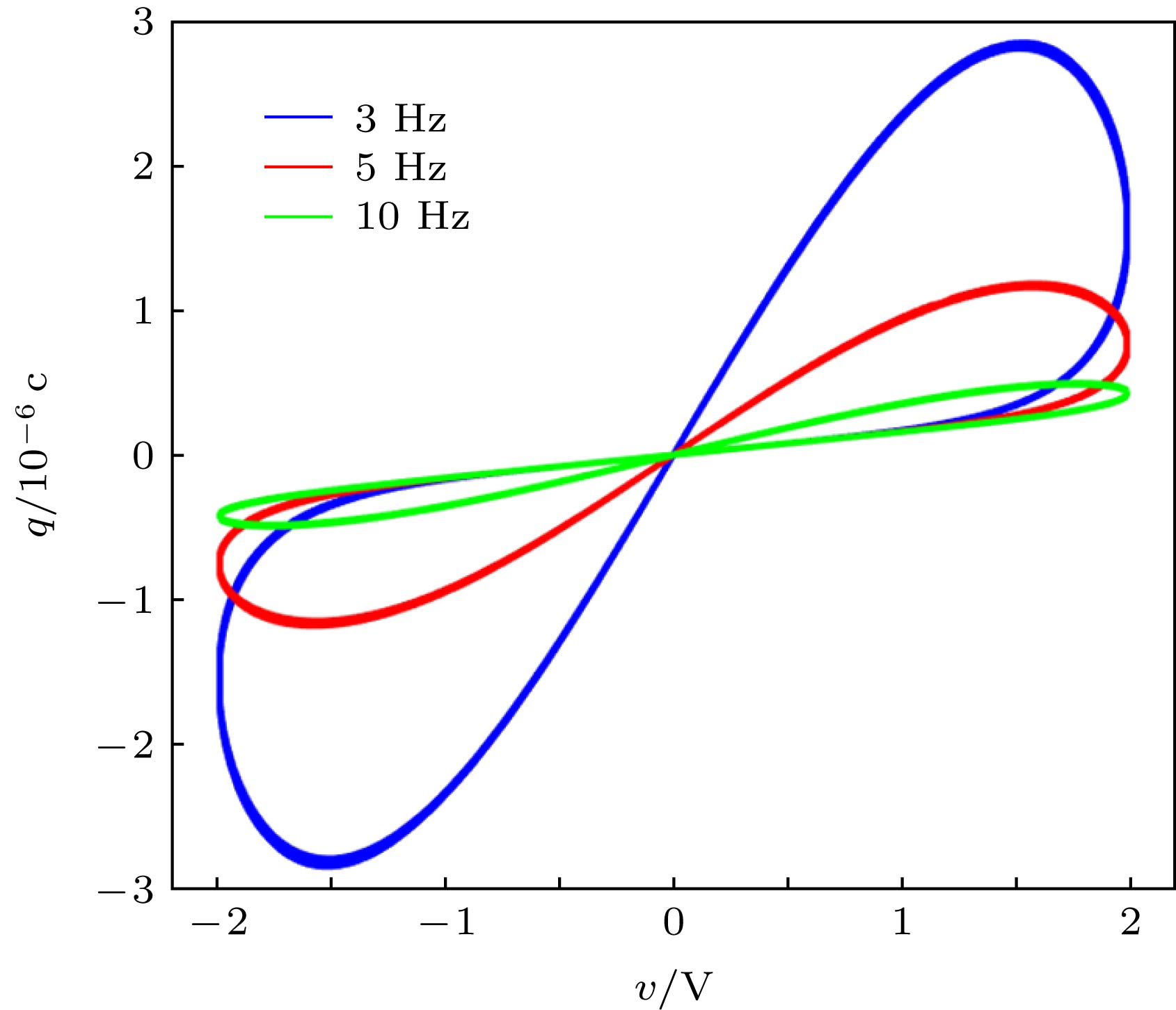 图 1 忆容器的q-v特性曲线


 图 2 正弦交流电激励下忆容器


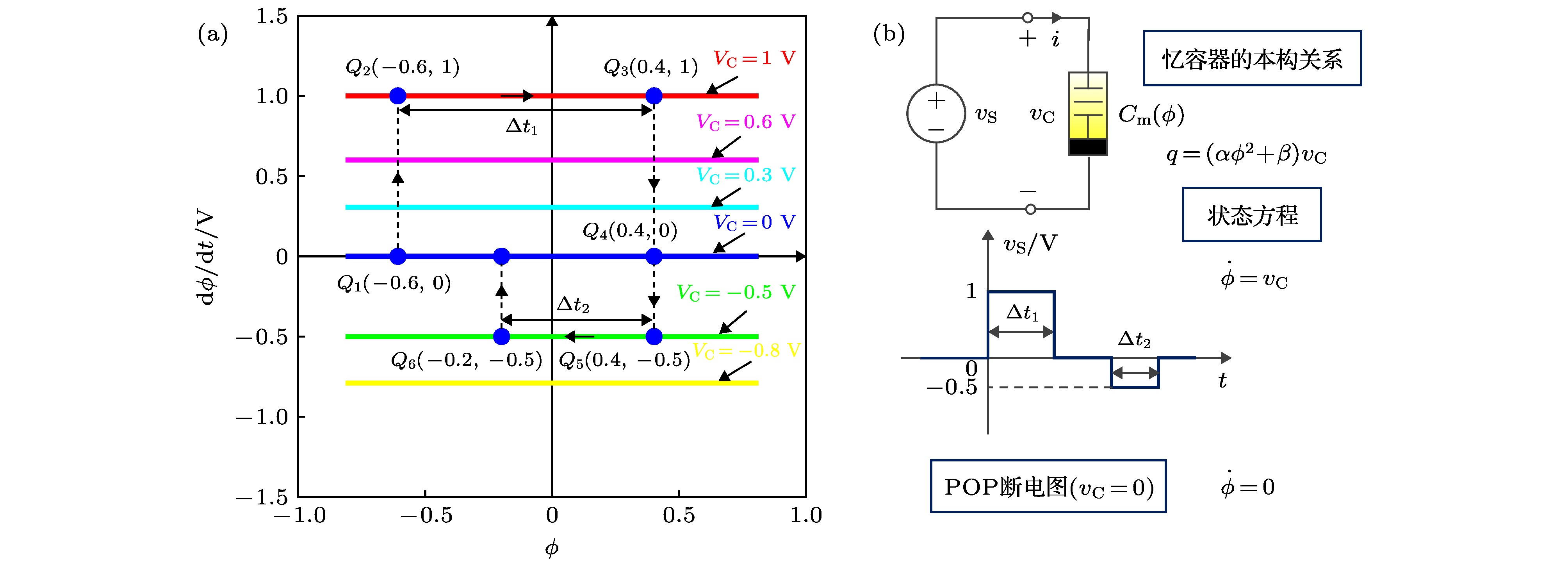 图 3 忆容器的动态路径图(


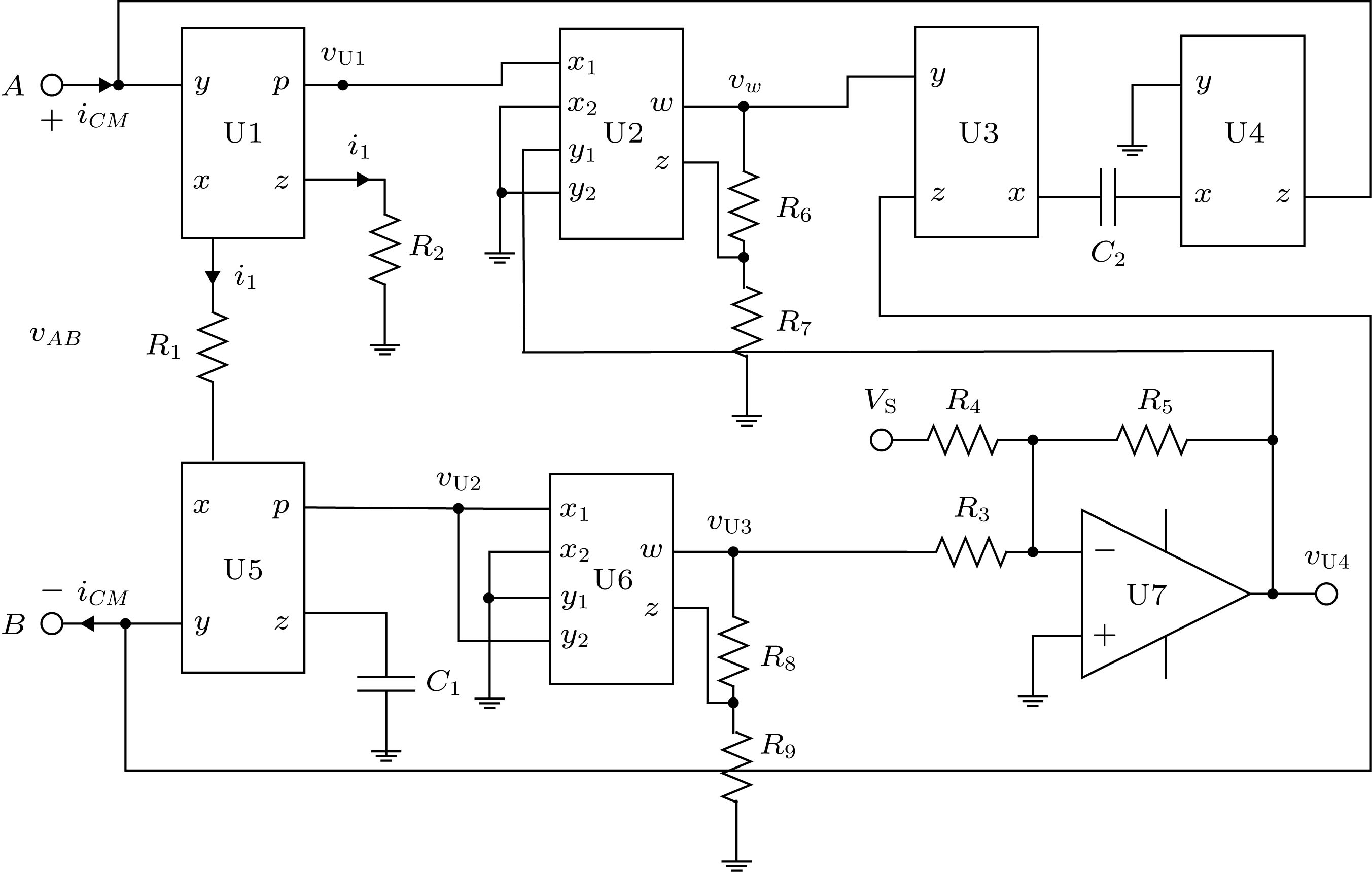 图 4 压控型忆容器仿真器


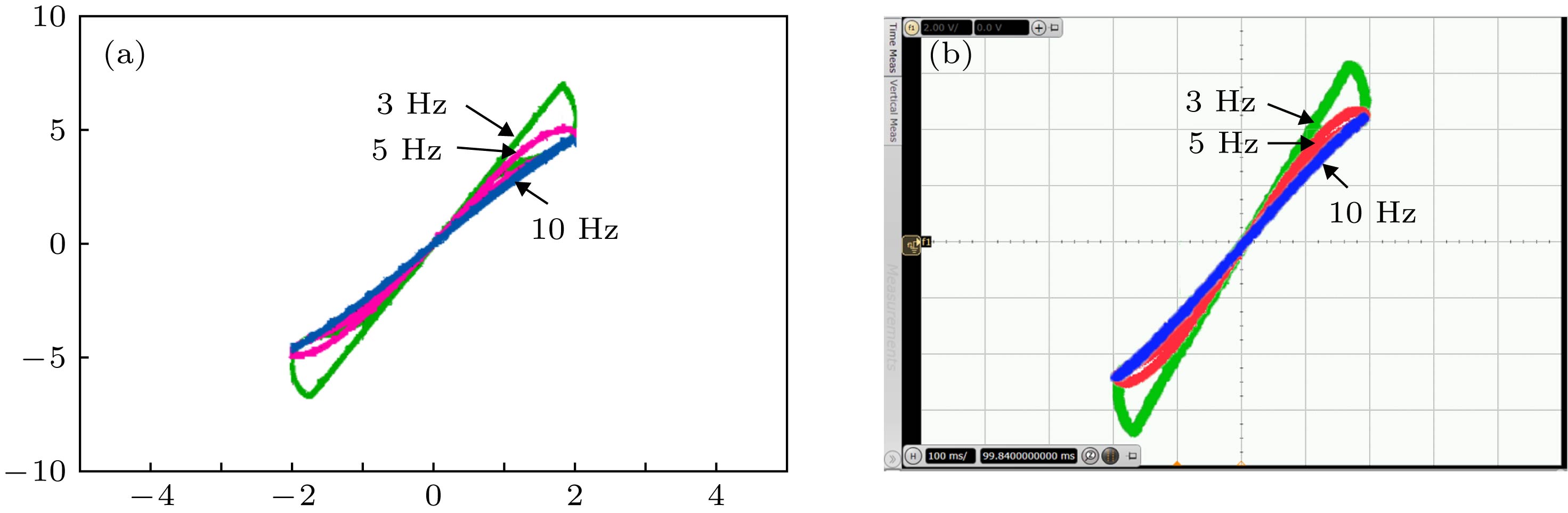 图 5 忆容器仿真器的


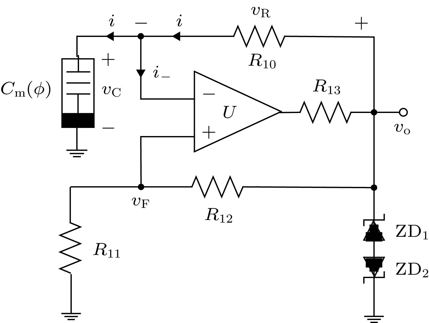 图 6 基于忆容器的多谐振荡器


 图 7
图 7 


 图 8 忆容器多谐振荡器仿真电路波形(


 图 9 硬件电路实测振荡波形(


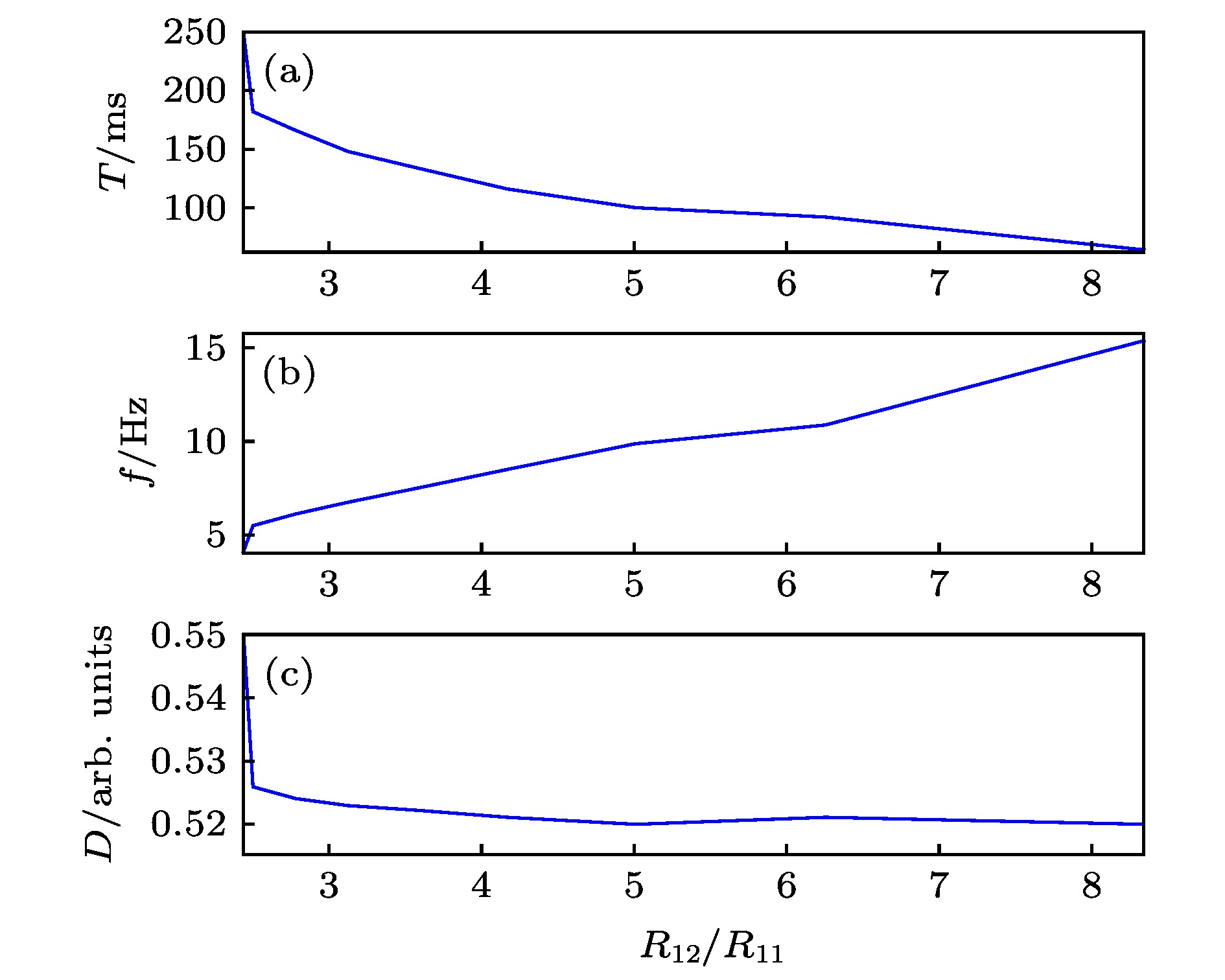 图 10
图 10 

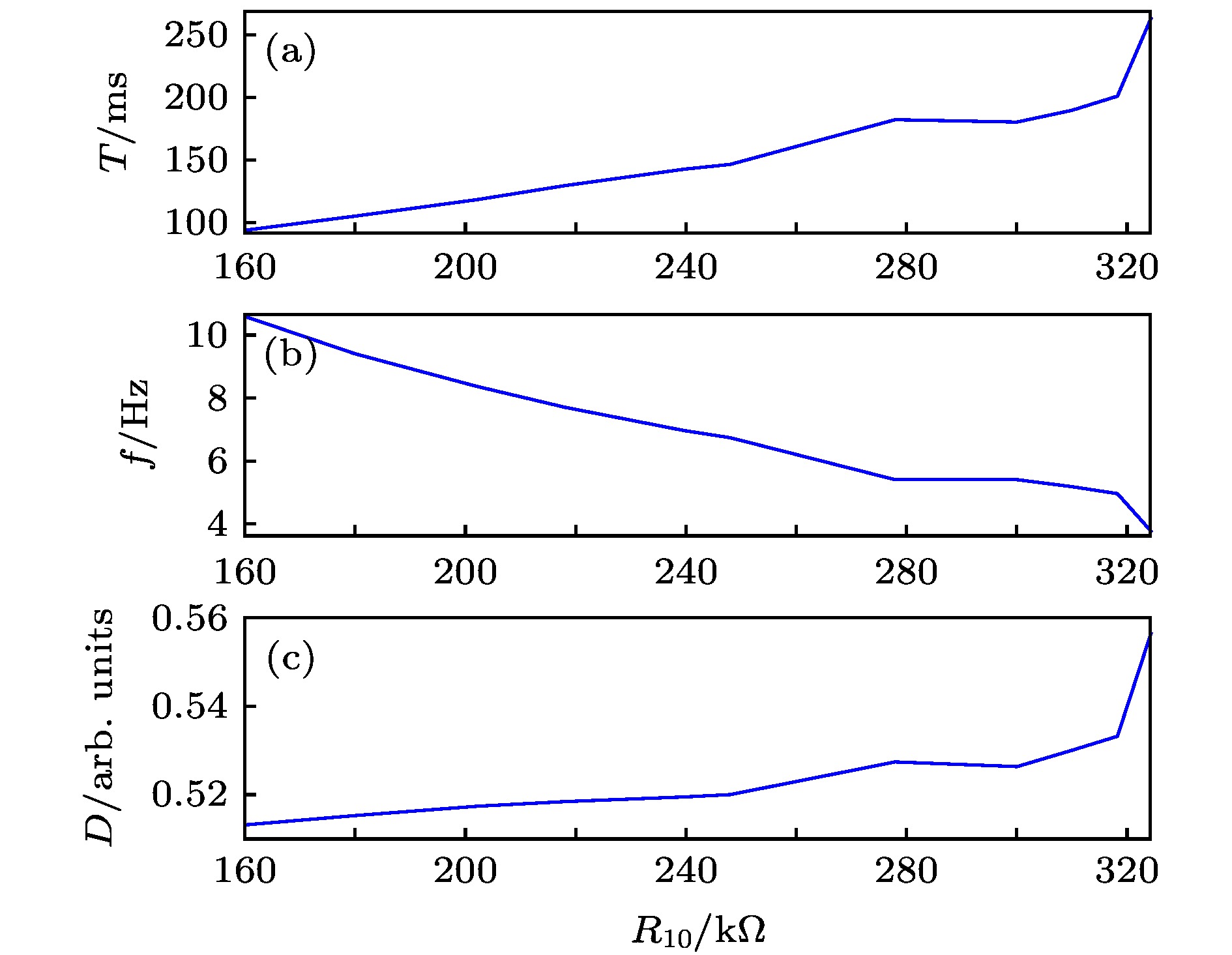 图 11
图 11 

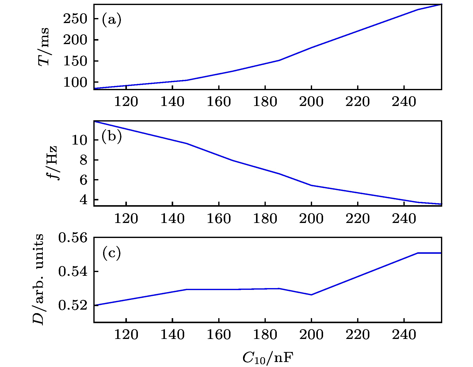 图 12
图 12 


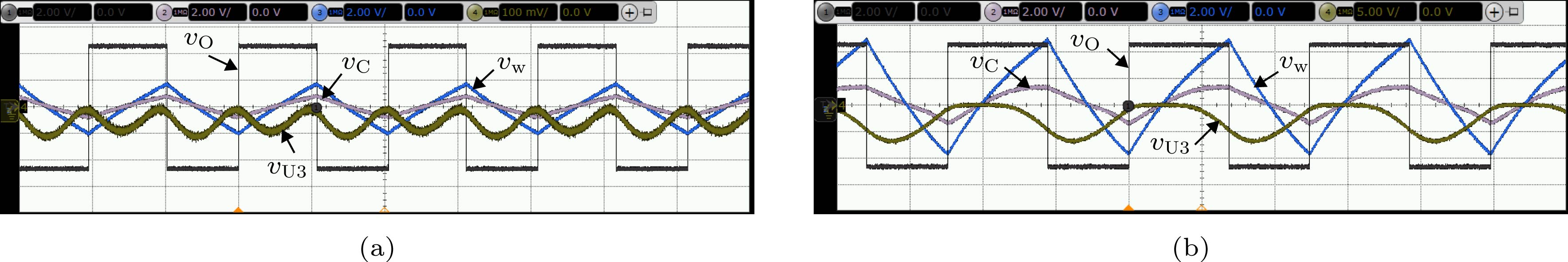 图 13 忆容器振荡器硬件电路实验振荡波形(图(a)和(b)中


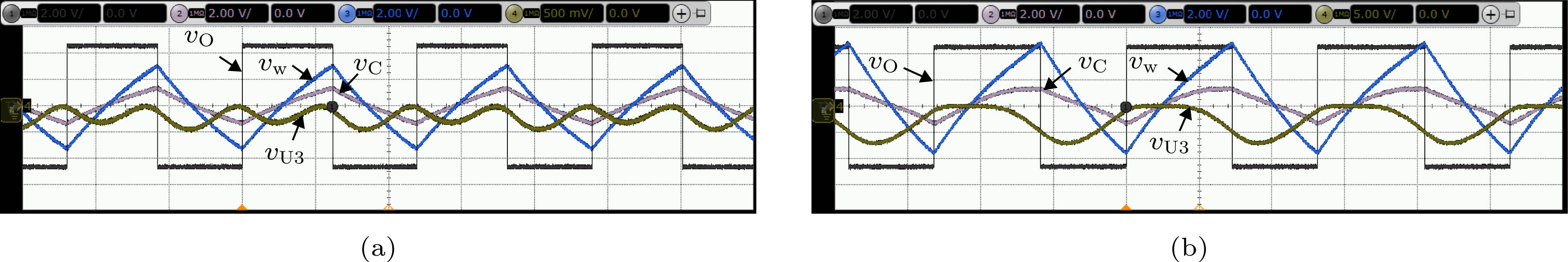 图 14 忆容振荡器硬件电路实验振荡波形(图中


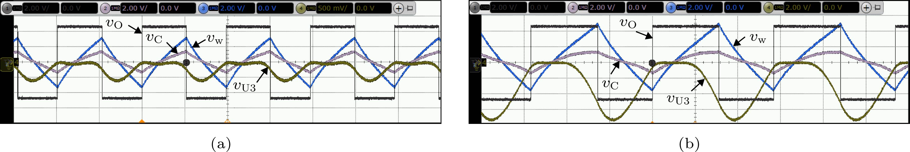 图 15 忆容振荡器硬件电路实验振荡波形(图中


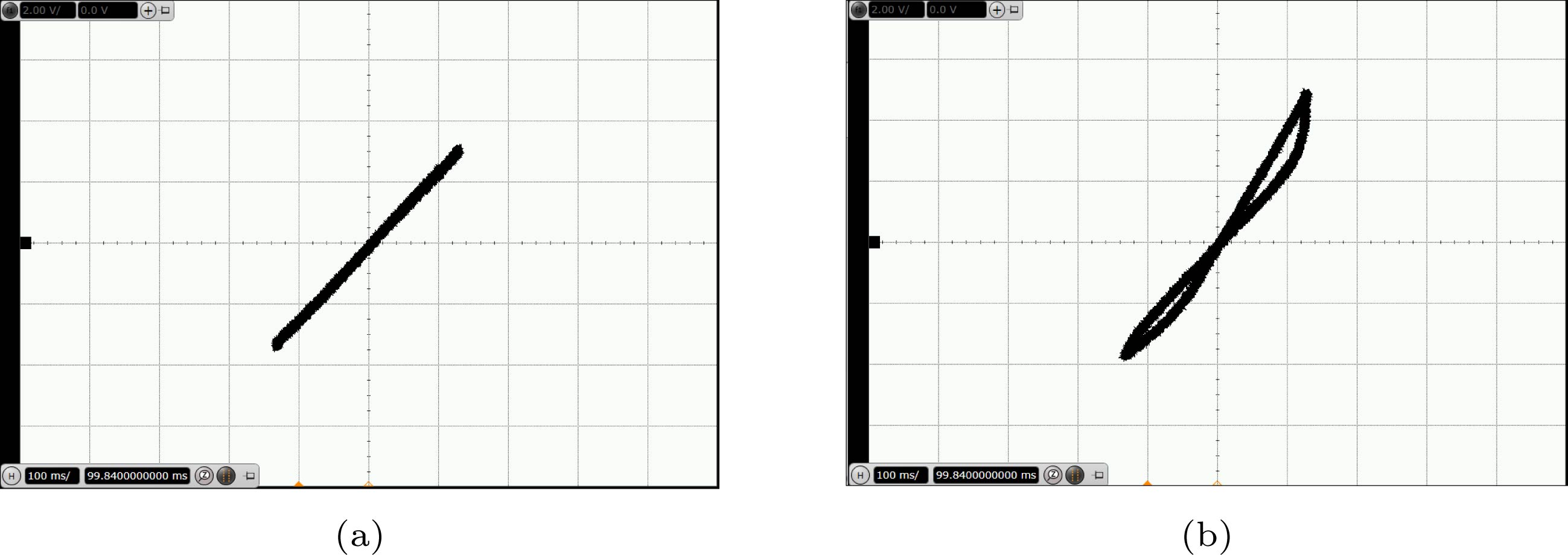 图 16
图 16 


