全文HTML
--> --> -->离子凝胶(ion-gel)是一种具有离子导电性的固态混合物, 具有很好的热稳定性和电导性. 在外电场作用下离子凝胶内部发生电荷不均匀分布, 与外部绝缘层表面的电荷层形成双电荷层分布, 这种结构可用古伊-查普曼-斯特恩(Gouy-Chapman-Stern, GCS)模型来解释(图1), 介电层中的离子和外部绝缘层表面电荷之间的附着主要依靠静电作用[16]. 双电层和传统电容器在电场作用下产生的电容效应相似, 紧密的双电层近似于平板电容器. 相比普通介质层材料具有更大的电容值, 在微米级的厚度下就具有μF/cm数量级的单位面积电容[14,17].
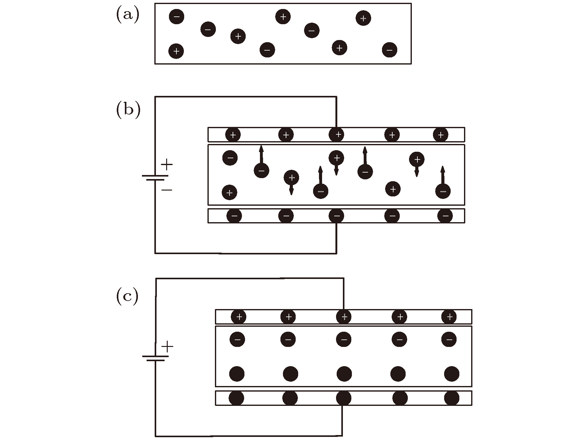 图 1 GCS模型双电荷层分布示意图 (a) 阴阳离子分散在电介质中; (b) 在外电场作用下, 电介质内部阴阳离子开始向两级移动; (c) 达到平衡后, 电介质内阴阳离子排布情况
Figure1. Schematic diagram of GCS model with dual-charge layer distribution: (a) The anions are dispersed in dielectric; (b) under the action of electric field, the anions and cations begin to move in the opposite direction; (c) the distribution of anions and cations in dielectric in equilibrium
本文将以ion-gel(PVDF-[EMIM]TF2N)薄膜作为底栅介质层材料, 制备底栅型GFET, 同时与以SiO2作为栅介的GFET进行对照, 依据电学特性曲线分析离子凝胶薄膜对GFET的跨导、开关比以及狄拉克电压等电学特性的影响, 同时研究真空环境和温度对离子凝胶薄膜栅介的GFET性能的影响.
2.1.GFET制备
1)栅介制备. 本实验制备的离子凝胶薄膜栅介采用溶液法制备, 将配置好(PVDF, [EMIM]TF2N和DMF质量体积比为4 : 1 : 40)的离子凝胶溶液旋涂(3000 r/min, 15 s)在ITO玻璃表面(图2(b)), 160 ℃烘干(30 min)后离子凝胶膜呈透明状(图3(a)), 台阶仪测试膜厚为2 μm. 2)石墨烯转移. 采用湿法转移[18,19]将石墨烯转移至离子凝胶膜表面(图2(c))和硅片的SiO2表面. 3)电极制备. 采用热蒸发真空镀膜仪制备铝电极, 样品放入真空镀膜室, 真空度达到3 × 10⁻³ Pa时开启热蒸发镀膜仪, 掩膜版源漏极之间距离0.5 mm (沟道长度), 铝膜蒸镀厚度为100 nm (图2(d)).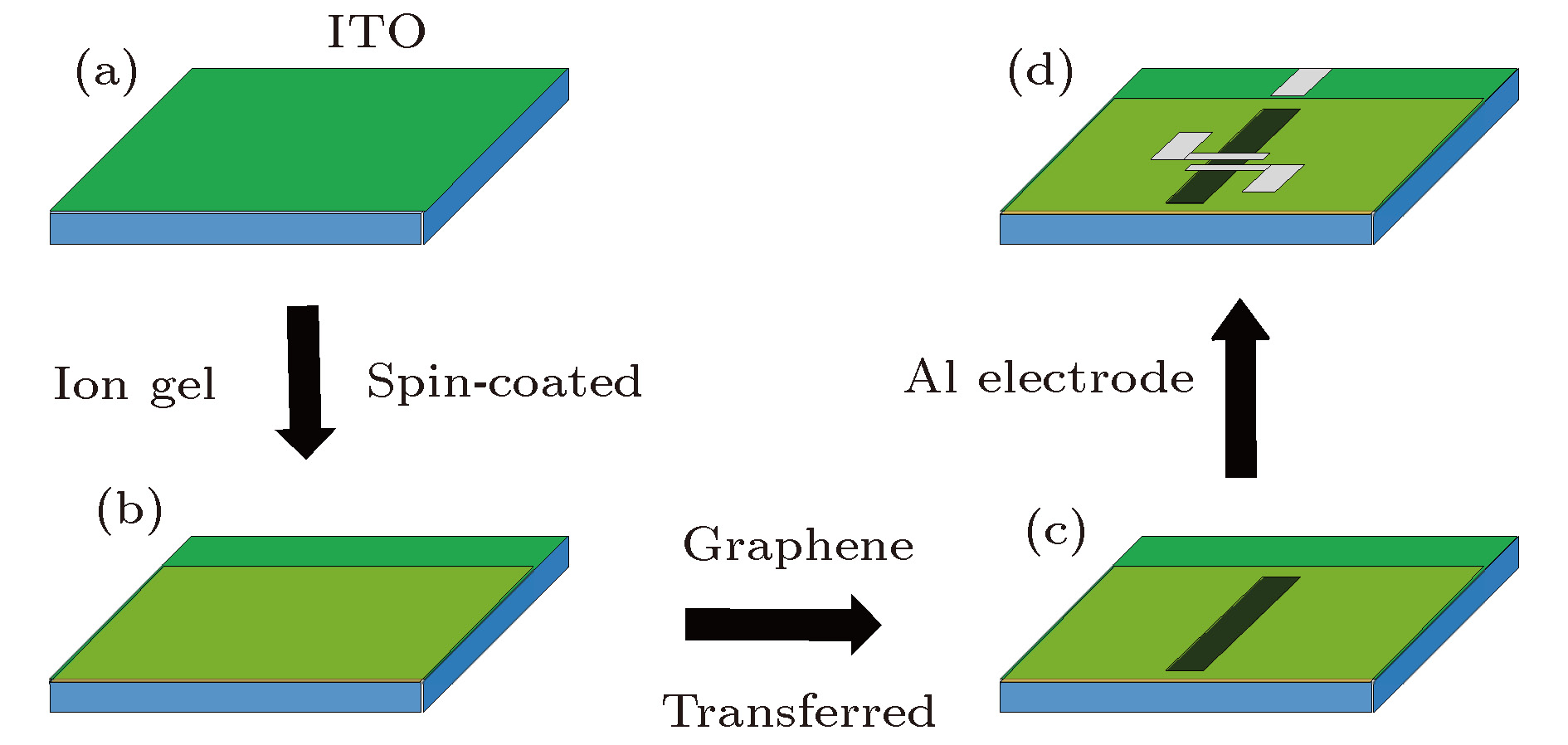 图 2 离子凝胶栅介的GFET制备过程
Figure2. Preparation of GFET with ion-gel film gate
 图 3 离子凝胶膜 (a) 离子凝胶膜呈透明状; (b) [EMIM]TF2N分子式; (c) PVDF分子式
Figure3. Ion-gel film: (a) Ion-gel film image; (b) molecular formula of [EMIM]TF2N; (c) molecular formula of PVDF
2
2.2.石墨烯表征
采用RENISHAW0963G1型拉曼光谱仪和SIGMA500型场发射扫描电子显微镜(SEM)对转移石墨烯前后的离子凝胶薄膜进行表征, 验证石墨烯是否成功转移.2
2.3.电学特性检测
制备完成后利用Keithley 2612a双通道数字源表对GFET的电学特性曲线进行测量, 电学检测示意图如图4所示. 首先在室温环境(25 ℃, 1 atm (1 atm = 1.01325 × 10⁵ Pa))下对离子凝胶膜栅介GFET和SiO2栅介GFET进行转移特性曲线和输出特性曲线的测量对比分析; 然后将离子凝胶膜栅介GFET放入真空干燥箱中, 真空度达到100 Pa (1 × 10⁻³ atm)时维持最低真空度, 通过测量电学特性曲线变化来检测GFET的狄拉克电压、跨导和开关比等电学特性与在真空环境中停留时间(5, 10, 20, 30 min)的关系; 当在真空环境中不再变化时, 逐渐升高温度, 检测GFET电学特性在不同温度(25, 50, 75, 100, 125 ℃)中的变化. 图 4 离子凝胶栅介的GFET电学检测示意图
Figure4. Schematic diagram of GFET with ion-gel film gate
3.1.拉曼表征
黑色曲线为离子凝胶膜基底的拉曼光谱, 仅在2980 cm–1处有明显的峰, 且与石墨烯的特征峰不重合. 红色曲线为转移至离子凝胶膜上的石墨烯的拉曼光谱, 从图5可以清楚地看到石墨烯在1580和2680 cm–1处的拉曼特征峰, 这是石墨烯原子晶格振动产生的特征峰G峰和2D峰[20], 说明石墨烯已成功转移至离子凝胶膜表面, 同时2D峰处呈现出完美的单个洛伦兹峰, 表明转移的石墨烯是单层的.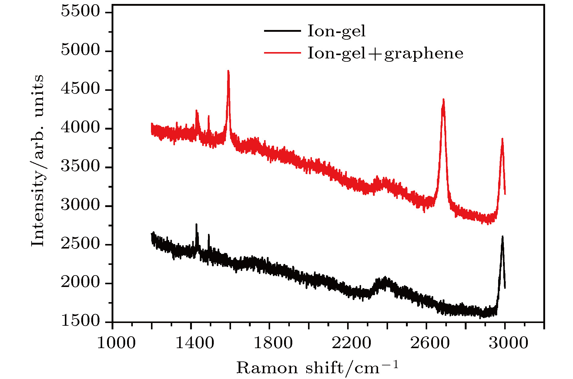 图 5 离子凝胶膜表面石墨烯拉曼光谱, 其中红线为转移石墨烯后的离子凝胶膜拉曼曲线, 黑线为未转移石墨烯的离子凝胶膜拉曼曲线
Figure5. Roman spectra of graphene on ion-gel. Red line corresponds to the ion-gel film with transferred graphene. Black line corresponds to the ion-gel film without graphene
2
3.2.扫描电子显微镜表征
图6为离子凝胶膜表面的SEM图像和转移石墨烯后离子凝胶膜表面的SEM图像. 通过图像对比可以看出, 石墨烯转移至离子凝胶膜后完全贴合在膜表面, PMMA基本去除干净, 石墨烯表面基本完整. 图 6 离子凝胶膜表面石墨烯SEM图像 (a) 未转移石墨烯的离子凝胶膜表面; (b) 转移石墨烯后的离子凝胶膜表面
Figure6. SEM images of ion-gel film: (a) The ion-gel film without graphene; (b) the ion-gel film with transferred graphene
2
3.3.电学特性
众所周知, 金属的导带和价带是重叠的, 半导体的导带和价带是分开的(有能带间隙), 而石墨烯的导带和价带刚好交于一点, 此点即为狄拉克点(图7(a)), 通过掺杂等手段可使石墨烯的能带打开(图7(b)), 进而提高开关比. 室温环境下GFET的转移特性曲线(图8(a))中的最低点对应的电压称为狄拉克电压(VDirac), 理论上在无栅极电压作用下(Vg = 0), 石墨烯沟道内载流子浓度达到最低, 电导率也达到最低; 然而图8中GFET转移曲线皆出现往右偏移, 主要是因为实验采用湿法转移石墨烯, 附着在表面的水分子和氧气能够束缚住σz轨道自由电子而表现出还原性电子转移[21-23], 相应位置产生空穴, 使得石墨烯出现p型掺杂. 以图9石墨烯能级示意图为例, 在Vg = 0时(图9(a)), p型掺杂的石墨烯的费米能级(EF)位于本征费米能级(EFi)之下, 平衡状态下仍存在少数空穴载流子, 形成弱p型沟道. 当Vg < 0时(图9(b)), 石墨烯导带能级(Ec)和本征费米能级进一步远离费米能级, 而价带能级(Ev)更接近于费米能级, 此时沟道内部产生空穴堆积, 形成强p型沟道; 当0 < Vg < VDirac时(图9(c)), 石墨烯本征费米能级接近费米能级, 此时沟道内的少数空穴载流子被中和, 导电性最低; 当Vg > VDirac时(图9(d)), 石墨烯的费米能级位于本征费米能级之上, 导带能级更接近于费米能级, 沟道内部产生电子堆积, 形成n型沟道, 导电性回升. 图 7 石墨烯能带示意图
Figure7. Band diagram of graphene
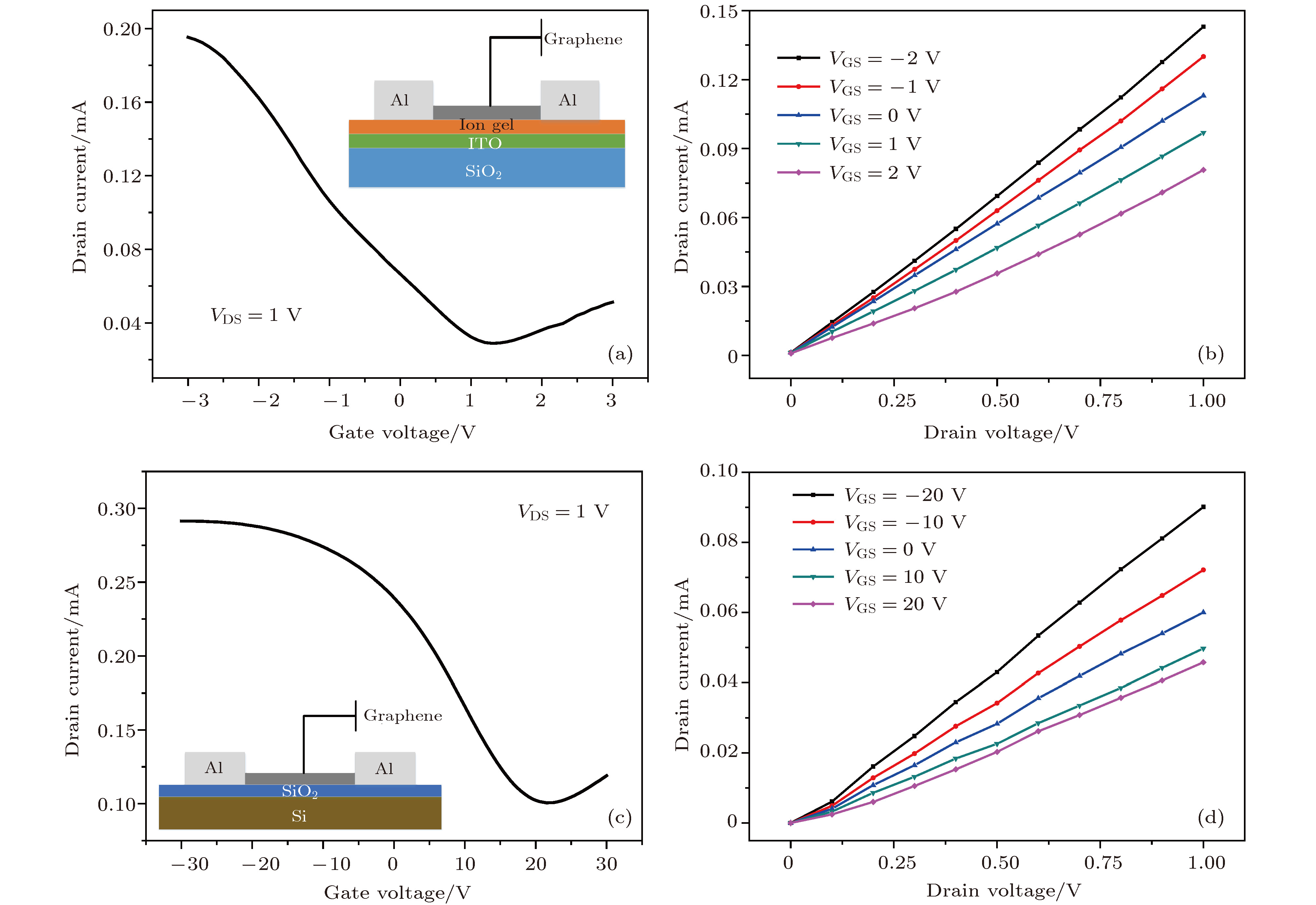 图 8 室温环境下GFET电学特性曲线 (a)离子凝胶栅介GFET的转移特性曲线; (b)离子凝胶栅介GFET的输出特性曲线; (c) SiO2栅介GFET的转移特性曲线; (d) SiO2栅介GFET的输出特性曲线
Figure8. Electrical characteristic curves of GFET at room temperature: (a) The transfer characteristic curve of GFET with ion-gel film gate; (b) the output characteristic curve of GFET with ion-gel film gate; (c) the transfer characteristic curve of GFET with SiO2 gate; (d) the output characteristic curve of GFET with SiO2 gate
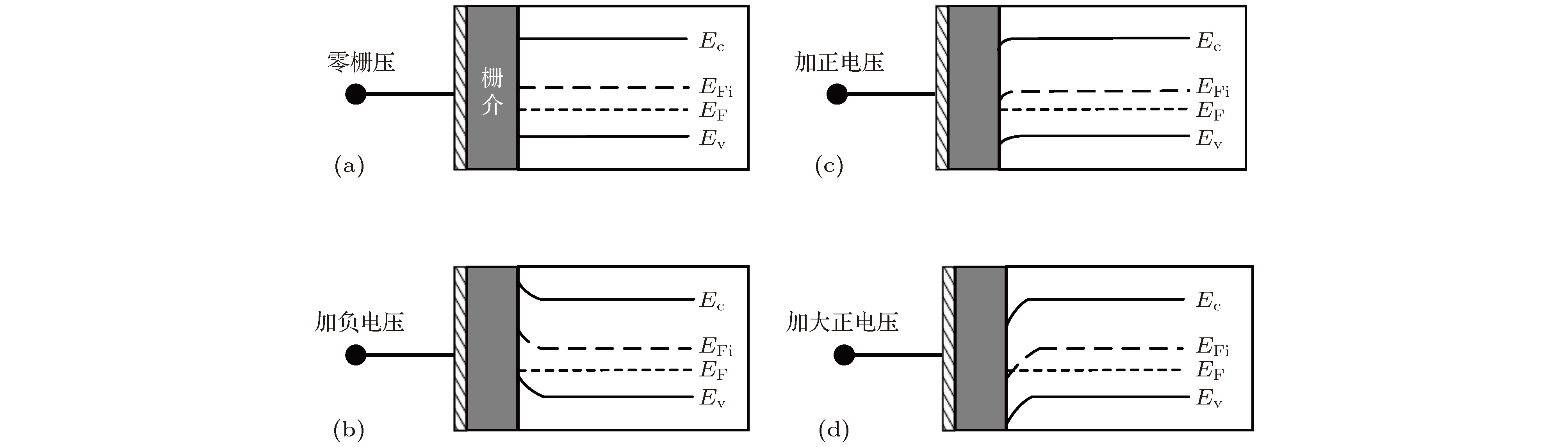 图 9 p型掺杂石墨烯能级示意图
Figure9. Energy level of p-type doped graphene
转移特性曲线中SiO2栅介GFET (图8(c))的狄拉克电压约在22 V, 而离子凝胶膜栅介GFET (图8(a))的狄拉克电压降低至1.3 V左右. 转移特性曲线的跨导(gm)根据I-V曲线最大斜率进行计算, 反映出栅极电压对源漏极电流的调控作用. 计算公式如下:


输出特性曲线中SiO2栅介GFET (图8(d))栅压变化范围为–20—20 V, 离子凝胶栅介GFET (图8(b))栅压变化范围为–2—2 V, 源漏电压(VDS)均控制在1 V以内. 可以看出源漏电流(IDS)随着Vg的改变而变化, Vg对IDS起着调控作用, 两者的IDS与VDS均呈线性关系, 说明石墨烯与电极之间为欧姆接触. 由综合转移特性曲线和输出特性曲线可以看出, 离子凝胶膜可以有效降低狄拉克电压, 提高GFET跨导和开关比, 同时降低控制电压范围, 从而提高GFET电学性能.
2
3.4.空气对GFET的影响
底栅型GFET最大的特点是石墨烯上表面暴露于外界环境中, 空气中的水分子、氧气等杂质分子会吸附在石墨烯表面. 将GFET位于真空干燥箱内持续抽真空, 不断将腔室内的空气排除的同时也将附着在石墨烯表面的水分子、氧气等杂质分子进行脱附. 从GFET的转移特性曲线(图10(a))可以看出, 随着空气杂质分子脱附的进行, I-V曲线逐渐向左偏移, 狄拉克点也向零点方向偏移. 30 min以后GFET狄拉克电压达到最低0.4 V, 主要是因为空气杂质分子的脱附使得被捕获的σz轨道电子重新成为自由电子, 相应的空穴减少, 费米能级更接近于本征费米能级. 相关研究[11,12]采用的双栅极结构中在背栅电压施加前先在顶栅加载一定的电压, 相当于对石墨烯施加掺杂效应, 从而影响非工作状态下石墨烯沟道内的单一载流子(电子或空穴)浓度, 进而改变GFET的狄拉克电压和电流开关比. 而空气杂质分子产生的p型掺杂也仅属于弱掺杂, 对于GFET开关比的影响有限.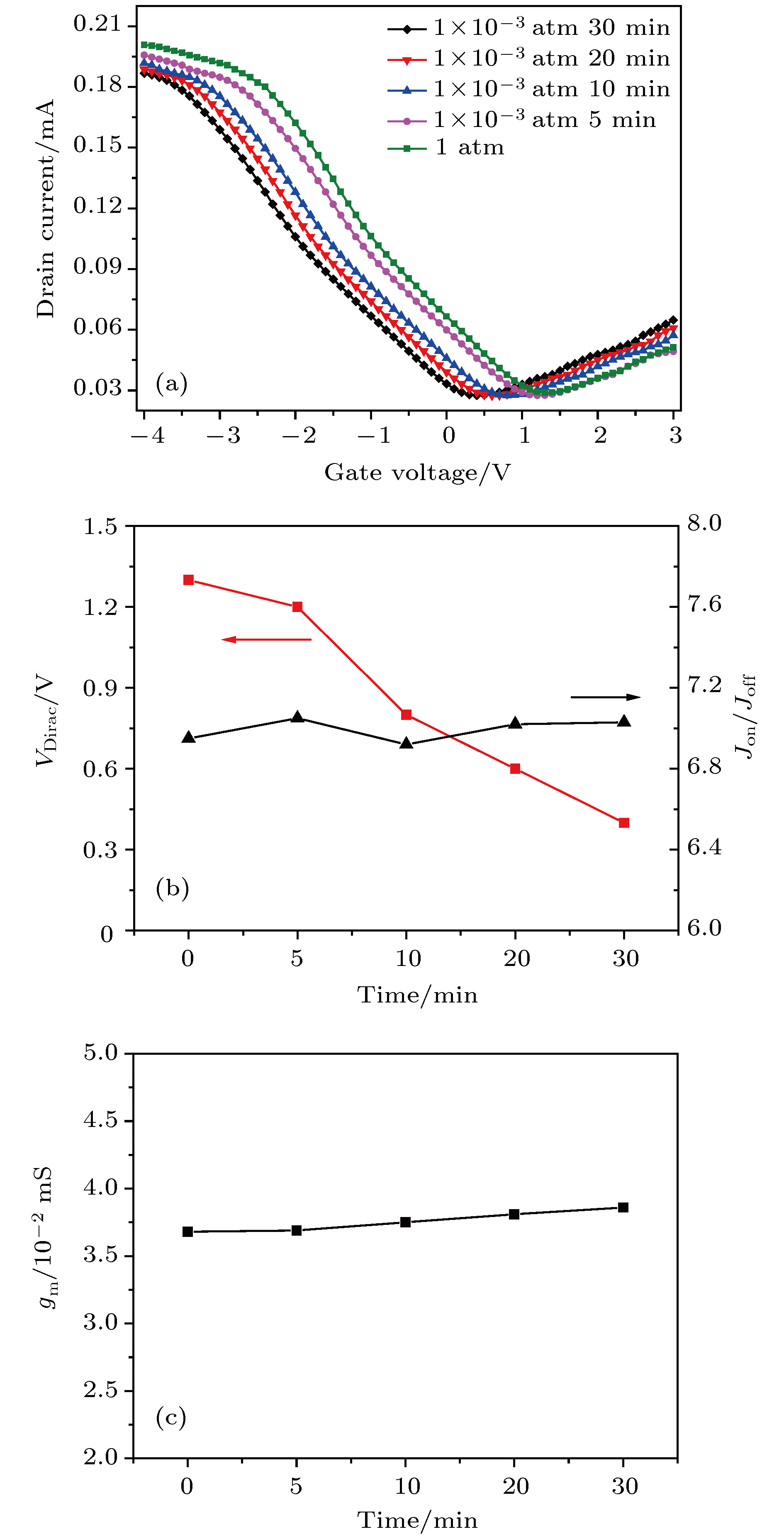 图 10 真空对GFET电学特性的影响 (a) 转移特性曲线; (b) 狄拉克点电压和开关比; (c) 跨导
Figure10. Effect of vacuum on the electrical properties of GFET: (a) Transfer characteristic curve; (b) Dirac point voltage and current switching ratio; (c) transconductance
2
3.5.温度对GFET的影响
温度对GFET电学特性的影响如图11所示. 在真空环境下排除空气杂质分子的干扰后, 逐渐升高温度, 狄拉克电压基本没有变化, 而在相同栅压下电流值逐渐升高. 根据I-V曲线对GFET的跨导进行计算, 可以得到在温度升高至125 ℃时跨导达到最大, 为6.11 × 10⁻² mS. 电导率的大小决定于半导体载流子浓度和载流子迁移率, 随着石墨烯表面杂质脱附, 受掺杂效应的影响降到最低, 所以随着温度升高本征激发开始起作用, 载流子浓度开始增大, 而迁移率会随温度的升高而降低(晶格振动加剧, 导致声子散射增强所致); 晶体管中的栅介离子凝胶膜却因为温度升高, 非晶体系中的离子扩散更容易[24], 电容值也会随之升高, 进而会提高石墨烯的载流子迁移率来抵消因为温度升高造成的影响, 所以晶体管的电导率会逐渐升高. 温度对狄拉克电压和开关比影响不明显, 可能是石墨烯能带的变化受温度影响有限, 而更多地与自身缺陷掺杂有关[25-27].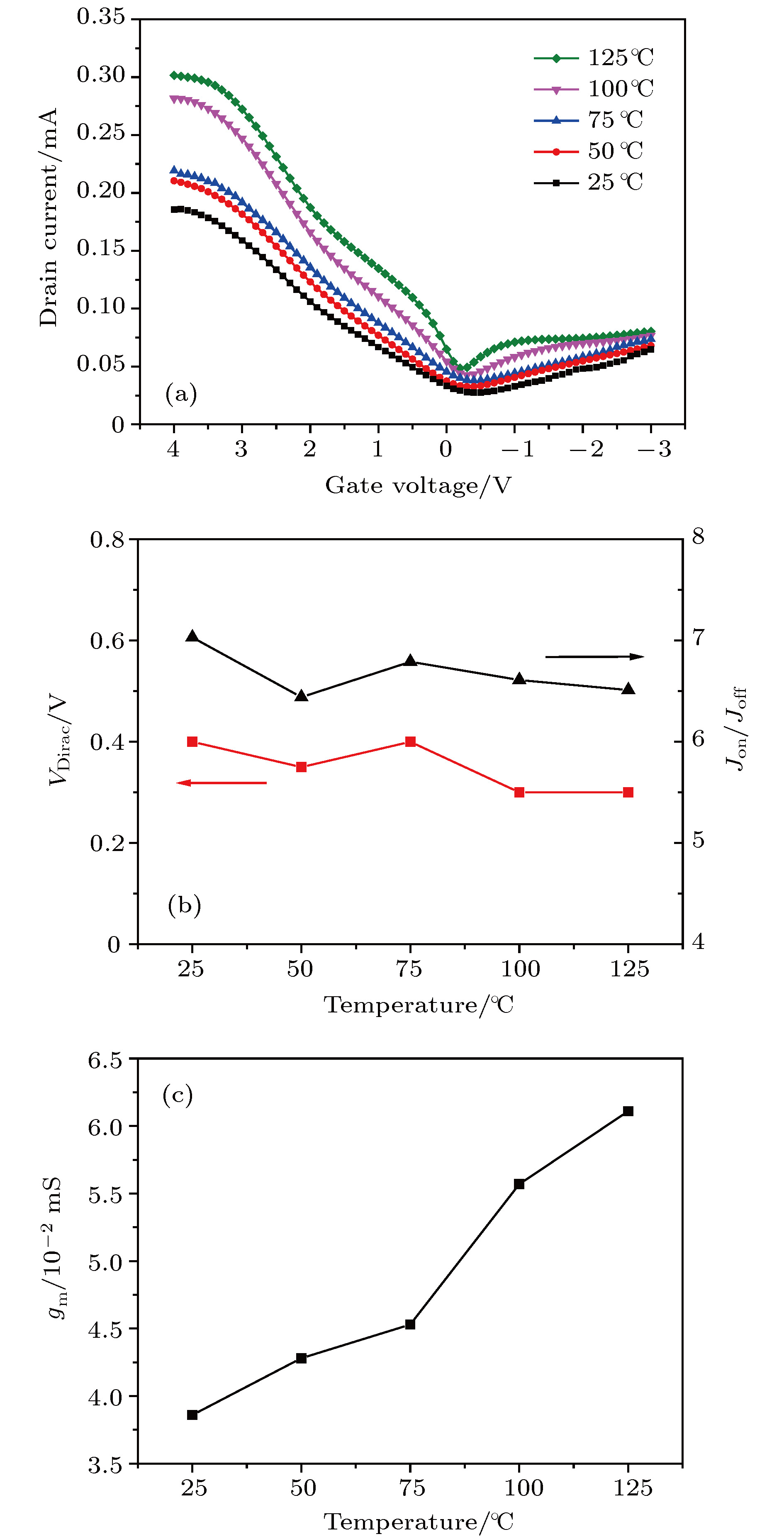 图 11 温度对GFET电学特性的影响 (a) 转移特性曲线; (b) 狄拉克点电压和开关比; (c) 跨导
Figure11. Effect of temperature on the electrical properties of GFET: (a) Transfer characteristic curve; (b) Dirac point voltage and current switching ratio; (c) transconductance
