Key Laboratory of Materials Modification by Laser, Ion, and Electron Beams, Ministry of Education, School of Physics, Dalian University of Technology, Dalian 116024, China
Fund Project:Project supported by the National Natural Science Foundation of China (Grant Nos. 12020101005, 11975067)
Received Date:22 March 2021
Accepted Date:24 April 2021
Available Online:28 April 2021
Published Online:05 May 2021
Abstract:The capacitive CF4/Ar discharges driven by a dual frequency source based on the electrical asymmetry effect (EAE) are studied by using a one-dimensional fluid coupled with Monte-Carlo (MC) model and a two-dimensional trench model. The effects, induced by varying the relative gap distance, on self-bias voltage, electronegativity, ion flux, neutral flux and other plasma characteristics are systematically discussed. In this asymmetric discharge, as the gap distance increases, the absolute value of the self-bias voltage and electronegativity decrease. Meanwhile, the plasma density and absorption power increase accordingly because the effective discharge area expands but the boundary loss is still limited. In addition, both $ \mathrm{\alpha } $ mode and drift-ambipolar (DA) mode can play their important roles in the discharges with different gap distances, though DA mode is weakened in large gap discharge. Owing to the fact that the self-bias is larger and electronegativity is stronger for the case of smaller gap distance, the sheath expansion electric field at the powered electrode and the bulk electric field heat the electrons, leading the ionization rate to greatly increase near the collapse of the sheath at the grounded electrode. Besides, at the larger gap distance, the maximum value of the ionization rate decreases due to the reduction of electrons with relatively high-energy, and the ionization rate near the grounded electrode is reduced evidently. Moreover, with the increase of the gap distance, the maximum ion energy decreases and the ion energy distribution width becomes smaller due to the reduction of the self-bias voltage. Meanwhile, the etching rate increases a lot since the neutral flux increases significantly near the powered electrode. However, as the gap distance increases to 5 cm, the etching rate stops increasing and the trench width at the bottom becomes narrow because the neutral flux increases greatly compared with ion flux, forming a thick layer of polymer. So, besides separately controlling the ion energy and flux, optimizing the synergistic effect of ion flux and neutral group flux to adjust the etching rate and improve the etching morphology is also an interesting topic in the asymmetric CF4/Ar discharges. Keywords:electrical asymmetry effect/ the synergy of ions and neutrals/ gap distance/ discharge mode
图 3 在不同电极间距(a) 3 cm, (b) 4 cm, (c) 5 cm下时空演化的电子密度 Figure3. Spatio-temporal evolution of electron density for different gap distance of (a) 3 cm, (b) 4 cm, (c) 5 cm.
图5给出了时空演化的体区电场在不同电极间距下的变化情况. 受非对称电压波形影响, 除了在基频周期下随着鞘层扩张和回缩, 体区电场出现峰值, 在半个基频周期附近, 随着鞘层振荡也会出现局域的次峰值. 特别是在间距小的情况下, 电负性强、体区电子密度低、电导性差, 为维持放电导致体区电场增强, 这种现象就更加明显. 随着电极间距的增加, 体区电场逐渐变弱, 但是峰值仍然存在. 经过计算发现, 随着电极间距的增加体区压降变化不大, 分别为0.619, 0.44, 0.369 V, 但是体区有效放电宽度增大, 分别约为2.07, 2.96, 3.95 cm. 此外, 还可以看到, 当间距为3 cm时, 由于电负性较强, 不仅体区电场强, 在鞘层附近, 特别是接地电极处在0.25 T到0.75 T时间范围内出现较强的双极扩散场, 其峰值绝对值可达到–11.5 V/cm左右; 而当间距为5 cm时, 体区电场变弱的同时, 电场在功率极板附近的峰值相对比较容易观察到(0.9 T), 大约7.5 V/cm. 图 5 在不同电极间距下时空演化的电场 (a) 3 cm; (b) 4 cm; (c) 5 cm Figure5. Spatio-temporal evolution of electric field for different gap distance of (a) 3 cm, (b) 4 cm, (c) 5 cm.
图6给出了在不同电极间距下时空演化的电子功率吸收($ {J}_{\mathrm{e}}\cdot E $)的变化情况. 通常, 容性耦合放电主要有$ \mathrm{\alpha } $模式和迁移扩散(DA)模式两种放电加热模式. 其中, 把鞘层振荡加热引起的放电模式称为$ \mathrm{\alpha } $模式, 而把电子在体区受到漂移场加速和鞘层附近受到双极性电场加速的放电模式称为DA模式, 后者通常发生在电负性气体放电中[41]. 从图6可以看出, 特别是间距在3 cm和4 cm时, 鞘层振荡加热、漂移场和双极电场加热都能明显观察到, 考虑到这里是Ar和CF4混合放电, CF4只占10%, 共同作用是合理的. 随着电极间距的增加, 体区电负性和电场都相对变弱, 导致了体区电子加热相应减小. 虽然放电空间大自偏压变低, 鞘层振荡仍然是主要的加热方式. 图7给出了在不同电极间距下电子能量分布函数(EEDF)基频周期平均空间演化情况. 从图7可以看出, 电极间距为3 cm时, 电子能量分布高能尾加强, 在体区和鞘层附近电子都可以获得相对较高能量, 与图5、图6中电场、电子加热时空分布相符. 图 6 在不同电极间距下时空演化的电子功率吸收 (a) 3 cm; (b) 4 cm; (c) 5 cm Figure6. Spatio-temporal evolution of electron power absorption rate for different gap distance of (a) 3 cm, (b) 4 cm, (c) 5 cm.
图 7 在不同电极间距下, 基频周期平均的电子能量分布函数(EEDF)的空间演化图 (a) 3 cm, (b) 4 cm, (c) 5 cm Figure7. Time averaged EEDF for different gap distance of (a) 3 cm, (b) 4 cm, (c) 5 cm.
图8给出了在不同电极间距下Ar电离率的时空演化情况. 这里的电离率是指电子连续性方程中与电离有关的电离源项, 电离率与电子和Ar的密度以及(2)式相对应的速率系数有关. 我们知道, Ar的电离阈值在15.7 eV, 只有能量高于该阈值的电子才能参与Ar的电离过程, 图8反映了高能电子的时空分布情况. 从图8可以看出, 放电模式始终是α和DA的混合模式. 对比来看, 在较小的放电间距时(例如3 cm和4 cm), 电离率在接地极板附近出现了最大值(图中红色圆圈位置), 呈现了比较强的电离过程. 在基频周期起始时刻, 功率电极附近鞘层开始扩张, 此时自偏压、体区电场最强, 电子受鞘层作用获得能量, 并同时受体区较强电场作用加速打向接地电极. 电子到达接地极板附近时正遇鞘层塌缩, 而且双极扩散场很强, 此时该位置电子密度也比较高, 所以电离率很快达到峰值. 但随着电极间距的增加, 自偏压减小, 体区电场变弱, 这种电子被加速并在接地极板附近发生集中电离的现象逐渐消失, 在极板间距为5 cm时就基本没有观察到这种现象. 此外, 如图8所示, 另外一个电离率峰值发生在功率极板附近电场峰值所在位置, 这个次电离峰值在不同的极板间距条件下都能被观察到. 通过分析发现, 这个峰值是接地极板鞘层扩张、体区加速、功率极板鞘层塌缩、双极扩散场加热电子所引起的. 但是, 可以看到, 在放电区域小的时候, 由功率极板附近鞘层扩张电子加速打到接地极板鞘层附近的电离相对较强, 而放电间隙较大时, 电离源项的最大值发生在功率极板附近. 图 8 在不同电极间距下时空演化的电离率(Ar+e→Ar++2 e) (a) 3 cm; (b) 4 cm; (c) 5 cm Figure8. Spatio-temporal evolution of ionization rate (Ar+e→Ar++2 e) for different gap distance of (a) 3 cm, (b) 4 cm, (c) 5 cm.
下面讨论与刻蚀相关的离子能量分布函数、离子和中性基团通量及刻蚀形貌. 图9给出了基频周期平均Ar+, ${\rm{CF}}_3^+ $, ${\rm{CF}}_2^+ $的离子能量分布函数在不同电极间距下的演化情况. 可以看出, 随着电极间距的增加, 离子能量的最大值会逐渐减小, 分别为122, 116, 114 eV. 这和自偏压有关, 自偏压越大离子在鞘层电场作用下获得更多能量的概率就会越大, 相应的能量分布展宽也会变窄. 此外, 还发现在电极间距为3 cm时, 离子能量分布函数更趋向于单能; 而随着电极间距增大, 离子能量分布呈现两个甚至3个能量峰值, 这种现象产生的原因比较复杂, 受多个因素的影响, 比如鞘层压降、离子和中性基团的碰撞及离子渡越鞘层的时间, 值得之后的工作来进一步研究分析. 图 9 在电极间距为(a) 3 cm, (b) 4 cm, (c) 5 cm下功率电极处的离子能量分布函数. Figure9. Ion energy distribution (IED) at the powered electrode for different gap distance of (a) 3 cm, (b) 4 cm, (c) 5 cm.
图10给出功率电极附近的离子通量和中性基团通量随着电极间距的变化图. 从图10可以看出, 随着极板间距的增大, 电离阈值较低(10—20 eV左右)的离子, 例如Ar+, ${\rm{CF}}_3^+ $, ${\rm{CF}}_2^+ $的通量值有略微增加, 而电离阈值相对大(20—35 eV左右)一些的离子CF+, F+, C+通量呈现一个减小的趋势. 从图7可知, 电离阈值较高的离子通量减小的原因主要是高能电子在放电区域大的时候所占的比率减小导致的. 而随着电极间距的增加, 实际馈入功率和等离子体密度都会相应增大, 电子密度有所上升导致电离阈值较低的离子通量有所增加. 各种中性基团通量同样呈现一个增加的趋势, 如图10(b)所示. 中性基团的解离能量阈值和Ar+, ${\rm{CF}}_3^+ $, ${\rm{CF}}_2^+ $的电离相当, 阈值都在10—20 eV范围内, 所以随着电极间距的增加, 中性基团通量的增加和Ar+, ${\rm{CF}}_3^+ $, ${\rm{CF}}_2^+ $通量的增加的原因类似, 是电子密度增加引起的. 图 10 功率电极附近基频周期平均的(a)离子通量和(b)中性基团通量在不同电极间距下的变化情况 Figure10. (a) Ion flux and (b) neutral flux at the powered electrode for different gap distance.
图11给出了在不同电极间距刻蚀时间均为70 s下的刻蚀形貌图, 其中白色位置是材料被移除的位置, 浅灰色表示光刻胶, 黑色表示SiO2, 其他颜色表示钝化层、聚合物. 在相同的刻蚀时间下, 刻蚀的深度越深, 说明在该条件下的刻蚀速率越快. 从图11可知, 随着电极间距的增加, 刻蚀速率先增加后减小. 我们知道中性基团通量明显增加, 比如CF2和CF, 一方面增加钝化层的覆盖度, 加速目标材料的刻蚀, 另一方面, 如果中性基团过多就会形成大量的聚合物附着在钝化层上面, 阻碍了离子对钝化层的刻蚀. 通常, 会利用变量$A= $$({\varGamma }_{{\mathrm{C}\mathrm{F}}_{2}}\!+\!{\varGamma }_{\mathrm{C}\mathrm{F}})/({\varGamma }_{{\mathrm{A}\mathrm{r}}^{+}}\!+\!{\varGamma }_{{\mathrm{C}\mathrm{F}}_{3}^{+}}\!+\!{\varGamma }_{{\mathrm{C}\mathrm{F}}_{2}^{+}}\!+\!{\varGamma }_{{\mathrm{C}\mathrm{F}}^{+}}{+\varGamma }_{{\mathrm{F}}^{+}}\!+\! {\varGamma }_{{\mathrm{C}}^{+}})$, 即功率极板处中性基团通量和离子通量的比值来解释刻蚀槽形貌的变化情况, 这里只有CF2和CF能参与生成聚合物. 随着电极间距的增加, A值分别为16.42, 30.68, 51.77, 这说明中性基团相比于离子的增加幅度更高, 这是因为中性基团的损失源项相比离子少所导致的. 从刻蚀形貌来看, 图11(a)和图11(b), A值从16.42增加到30.68, 中性基团增加并与离子协同, 使得刻蚀速率增加. 但是如果A值继续增大到51.77, 如图11(c), 刻蚀速率开始减慢, 聚合物在钝化层表面的覆盖削弱了离子对目标材料的刻蚀. 所以, 在电非对称波形下调节电极间距能够使离子和中性基团在一定程度上解耦, 有助于调节中性基团的覆盖度, 达到控制刻蚀速率及优化刻蚀形貌的目的. 图 11 在电极间距为(a) 3 cm, (b) 4 cm, (c) 5 cm下刻蚀形貌 Figure11. Etching profiles for different gap distance of (a) 3 cm, (b) 4 cm, (c) 5 cm.


 图 1 非对称双频电压波形图


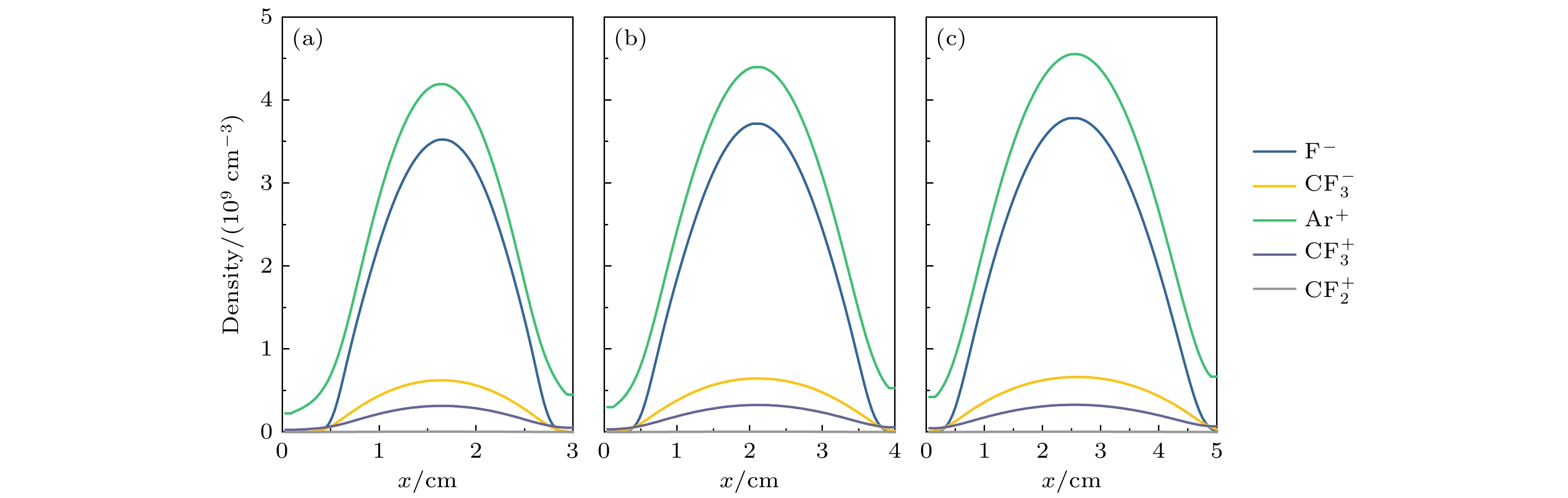 图 2 电极间距为(a) 3 cm, (b) 4 cm, (c) 5 cm下主要离子F–,


 图 3 在不同电极间距(a) 3 cm, (b) 4 cm, (c) 5 cm下时空演化的电子密度


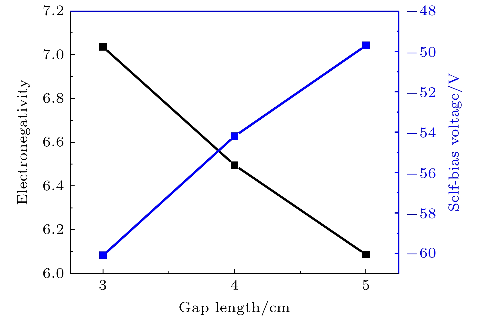 图 4 不同电极间距下的自偏压以及时空平均的电负性
 图 5 在不同电极间距下时空演化的电场 (a) 3 cm; (b) 4 cm; (c) 5 cm


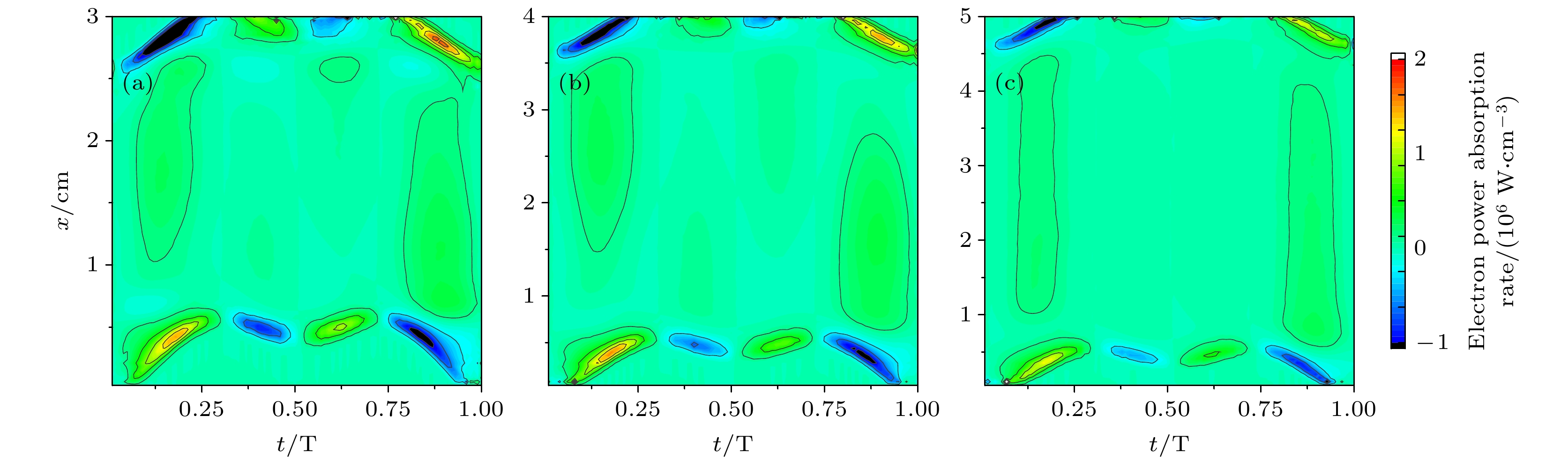 图 6 在不同电极间距下时空演化的电子功率吸收 (a) 3 cm; (b) 4 cm; (c) 5 cm
 图 7 在不同电极间距下, 基频周期平均的电子能量分布函数(EEDF)的空间演化图 (a) 3 cm, (b) 4 cm, (c) 5 cm
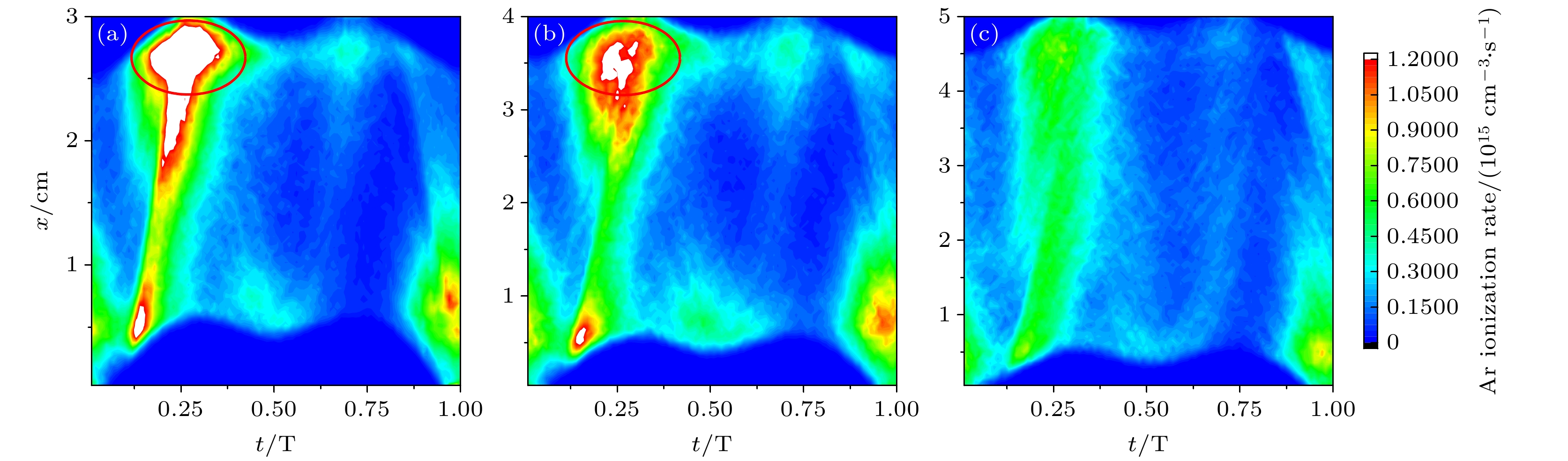 图 8 在不同电极间距下时空演化的电离率(Ar+e→Ar++2 e) (a) 3 cm; (b) 4 cm; (c) 5 cm

 图 9 在电极间距为(a) 3 cm, (b) 4 cm, (c) 5 cm下功率电极处的离子能量分布函数.


 图 10 功率电极附近基频周期平均的(a)离子通量和(b)中性基团通量在不同电极间距下的变化情况

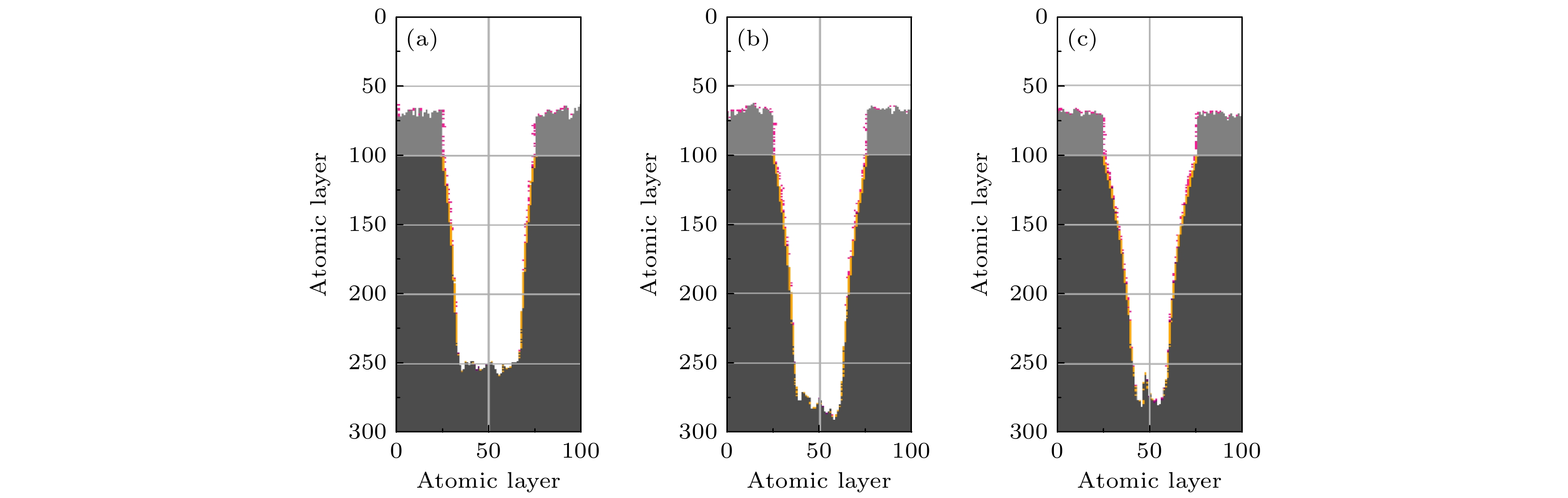 图 11 在电极间距为(a) 3 cm, (b) 4 cm, (c) 5 cm下刻蚀形貌
