1.School of Physics and Electronics, Central South University, Changsha 410012, China 2.State Key Laboratory of Powder Metallurgy, Powder Metallurgy Research Institute, Central South University, Changsha 410083, China 3.School of Physics and Technology, Xinjiang University, Urumqi 830046, China
Fund Project:Project supported by the National Natural Science Foundation of China (Grant Nos. 51272291, 52073308) and the Central South University Research Fund for Sheng-Hua Scholars, China (Grant No. 502033019)
Received Date:09 November 2020
Accepted Date:21 December 2020
Available Online:24 April 2021
Published Online:05 May 2021
Abstract:Based on the first principles calculations, the effects of substitutional doping of nitrogen, halogen and 3d transition metal elements on the electronic structure of monolayer Janus transition metal dichalcogenides WSeTe are studied in this paper, where the VASP software package is used based on density functional theory to perform calculations through using both the projector augmented wave method and the GGA-PBE functional method. A monolayer WSeTe hexagonal crystal system with 4 × 4 supercells is established, which contains 48 atoms. When VA (VIIA) element substitutes for monolayer WSeTe, one of the Se atoms is replaced with a nitrogen (halogen) atom; when the 3d transition metal element substitutes for monolayer WSeTe, one of the W atoms is replaced with a transition metal atom. Through the analysis of band structure, charge transfer and magnetism, it is found that VA (VIIA) nonmetallic elements doped monolayer WSeTe due to the introduction of the hole (electronic) doped, makes the Fermi level shift downward (upward), thus transforming into a p(n) type semiconductor. The Ti and V element substitutional doped monolayer WSeTe will present semiconductor-metal transformation. A doping for each of Cr, Co, Mn, Fe element doesn’t lead semiconductor material properties to change, but the each of Co, Mn, Fe element doped monolayer WSeTe can create a band gap of less than 20 meV. The VIIA (VA) non-metallic element and 3d transition metal element doped monolayer WSeTe will not have a huge influence on the original geometric structure of the material. Due to the charge transfer and doped atoms on the top of the valence band hybridization phenomenon, the Rashba spin splitting intensity near the Γ point of the top valence band increases with the increase of the atomic number of the doped atoms in the same main group when VIIA and VA non-metallic elements are doped. Moreover, the increase in atomic number and charge transfer have a greater influence on the strength of Rashba spin-orbit coupling than the change in electronegativity. The 3d transition metal element substitution doped single-layer WSeTe has obvious spin polarization phenomenon, which produces valley polarization near the Fermi level and introduces magnetism. In particular, since Cr-doped WSeTe retains the original semiconductor properties of WSeTe and has a large energy valley polarization, it may have a wide range of applications, such as in the field of spintronic devices. The monolayer WSeTe doped separately with Cr, Mn and Fe element produces an impurity band with fully polarized spin electrons in the band gap. The results are of great significance in systematically understanding the properties of monolayer WSeTe doping model and can provide theoretical reference for designing the monolayer WSeTe based electronic devices. Keywords:first principles calculation/ Janus WSeTe/ displacement doping
全文HTML
--> --> --> 1.引 言石墨稀、六方氮化硼(h-BN)、过渡金属硫族化合物(TMDs)、过渡金属氧化物和磷稀等二维材料由于其卓越的性能和丰富的物理化学性质[1-5], 为其应用和基础研究提供了可能性, 在太阳能电池、晶体管(场效应晶体管)、发光二极管、光电探测器、激光等新型电子和光电子器件中有非常理想的应用前景[6-11]. 在这些二维材料中, TMDs因其可调节的带隙以及独特的电子、光学和机械性能而备受关注[12]. Janus过渡金属硫族化合物由于两种硫族原子的电负性以及它们与过渡金属原子之间的键长存在差异使得二维材料产生了面外非对称的电势梯度, 这种面外电势梯度的不对称性引入了Rashba自旋劈裂[13,14]. 与其他单层的Janus过渡金属硫族化合物相比, 研究表明WSeTe具有更大的自旋劈裂[15], Janus过渡金属硫族化合物独特的性质使其在压电效应和自旋电子器件等诸多领域具有很好的应用前景. 通过化学气相沉积法, 用Se原子完全取代了MoS2的最上层所有S原子, 成功地合成了极性MoSSe[16]. 除此之外, 通过自下向上和自上向下的方法, 使用机械剥离、液相剥离、物理气相沉积、溶液化学过程和化学气相输运[17-20]等方法都可以成功制备Janus二维过渡金属硫族化合物. 已有的工作对单层Janus过渡金属硫族化合物在光催化剂、电子结构、磁性、声子输运以及析氢反应的催化[21-25]等方面都进行了广泛的研究. 原子替位掺杂是一种改变低维体系电子结构十分简单且有效的方式. 例如Cd掺杂使Bi2Se3薄膜由n型半导体到p型半导体的转变[26]. 在石墨烯中掺杂B和N原子在狄拉克点附近打开带隙[27]. 3d过渡金属元素掺杂在非磁的二维材料中引入磁性[28,29]等. 本文通过第一性原理计算系统地分析了VA (N, P, As, Sb)和VIIA (F, Cl, Br, I)非金属元素替换一个Se原子以及3d过渡金属(Ti, V, Cr, Mn, Fe, Co)元素替换一个W原子掺杂单层WSeTe超胞对电子结构的影响. VA (VIIA)非金属元素掺杂会引入空穴(电子); 3d过渡金属元素掺杂会破坏时间反演对称性从而引入磁性和能谷极化现象[30]. 2.计算模型与方法本文使用基于密度泛函理论(DFT)的VASP软件[31,32]包进行计算, 采用投影缀加平面波[33]和广义梯度近似下的Perdew-Burke-Ernzerhof (PBE)[34]泛函的方法同时设置截断能为400 eV. 为了消除周期性边界条件下其他原子对单层WSeTe的影响, 在Z轴方向上设置了一个20 ?的真空层. 能量的收敛标准设为10–5 eV, 力的收敛标准设为0.02 eV/?. 利用Monkhorst-Pack[35]方法对第一布里渊区进行采样, 由于超胞较大布里渊区K点网格设置为4 × 4 × 1. 在过渡金属元素替位W原子掺杂的计算中, 加入了自旋轨道耦合(SOC)并采用DFT + U的方法(Hubbard参数Ueff = 3 eV)[36]. 3.计算结果与讨论首先建立了一个单层WSeTe六角晶系的4 × 4超胞含有48个原子. 在VA (VIIA)元素替位掺杂单层WSeTe时将其中的一个Se原子替换为氮族原子(卤族原子); 在3d过渡金属(TM)元素替位掺杂单层WSeTe时将其中的一个W原子替换为过渡金属原子, 掺杂浓度为2.08%, 对x, y方向的晶格常数进行了优化, 所有结构都经过了充分弛豫. 如图1(c)所示, 一个没有掺杂的4 × 4 WSeTe超胞导带底和价带顶都处于K点, 是一个带隙为0.98 eV的直接带隙半导体, 与文献上计算得到的原胞能带结构符合较好[15]. 图 1 (a) VA (VIIA)和(b) TM元素替位掺杂单层WSeTe的俯视图(上)和侧视图(下)及其布里渊区和高对称点示意图; (c) 4 × 4的单层WSeTe超胞的能带结构 Figure1. (a), (b) The top view (top) and the side view (bottom) of the substitutionally doped monolayer WSeTe of VA (VIIA) and TM elements, as well as the schematic diagram of Brillouin zone and high symmetry points; (c) the energy band structure of 4 × 4 monolayer WSeTe supercell.
23.1.VIIA (VA)元素替位掺杂单层WSeTe -->
3.1.VIIA (VA)元素替位掺杂单层WSeTe
首先对VIIA (VA)元素替位Se原子掺杂单层WSeTe的结构进行了优化, 表1的结果表明Cl, Br, I, N, P, As, Sb掺杂后具有稳定的几何结构以及低的形成能$ {E}_{\mathrm{f}} $.
Doped atom
Se
Cl
Br
I
N
P
As
Sb
$ {d}_{\mathrm{W}-\mathrm{D}} $/?
2.570
2.547
2.680
2.826
2.021
2.424
2.555
2.799
$ {E}_{\mathrm{f}} $/eV
0
0.16
0.35
0.46
–0.48
–0.2
0.25
0.65
$ \Delta Q $/e
–0.47
–0.55
–0.46
–0.26
–1.23
–0.48
–0.24
–0.02
$ \alpha $/(eV·?)
0.21
0.18
0.19
0.22
0.04
0.13
0.14
0.21
表1未掺杂体系的Se原子或VA (VIIA)掺杂原子和W原子之间的键长$ {d}_{\mathrm{W}-\mathrm{D}} $、体系形成能$ {E}_{\mathrm{f}} $、掺杂原子得到的电荷数$ \Delta Q $以及Rashba常数$ \alpha $ Table1.Bond length $ {d}_{\mathrm{W}-\mathrm{D}} $ between VA (VIIA) doped atoms or Se atoms in an undoped system and W atoms, binding energy $ {E}_{\mathrm{f}} $, the number of charges obtained by doping atoms $ \Delta Q $ and Rashba constant $ \alpha $.
其中${E}_{\rm{D}\text{-}\rm{W}\rm{S}\rm{e}\rm{T}\rm{e}}$是原子替位掺杂WSeTe后的能量, $ {E}_{\mathrm{D}} $是一个孤立掺杂原子的能量, $ {E}_{\mathrm{W}\mathrm{S}\mathrm{e}\mathrm{T}\mathrm{e}} $是WSeTe超胞的能量, $ {E}_{\mathrm{S}\mathrm{e}\left(\mathrm{W}\right)} $是一个孤立的Se (W)原子能量. F原子半径较小且电负性较强使得F原子更多是以间隙掺杂或吸附的形式存在于WSeTe中, 因此F原子替位掺杂单层WSeTe无法优化得到一个稳定的结构. 随着原子序数的增大, VIIA (VA)掺杂原子与W原子之间的键长$ {d}_{\mathrm{W}-\mathrm{D}} $会逐渐增加. VIIA元素替位掺杂单层WSeTe时由于卤族元素最外层比Se原子多了一个电子, 因此卤族元素替位掺杂WSeTe相当于引入了电子掺杂并且能带中的费米能级上移到了原本导带底的位置使得材料变为n型半导体. 图2(a)中使用PBE + SOC方法得到的掺杂后的能带结构仍然保留了较宽的禁带, 只有导带底K点附近较窄的区域穿过费米能级. 通过对比Cl, Br, I掺杂后的能带结构图可以发现, 随着原子序数的增大, 加入SOC得到的能带中最高占据态(最低未占据态)会略微上(下)移, 减小禁带宽度. 从单个原子的投影态密度(PDOS)图2(d)可以看出, 费米能级附近能带主要来源于材料本身W原子的贡献. 由于掺杂浓度较低且掺杂原子对费米能级附近能带贡献较小, 不同的卤族元素掺杂时能带结构并没有明显的变化. 为了了解VIIA元素掺杂过程中电荷的转移情况, 计算了它们的差分电荷密度图, 从图2(e)可以发现, 电荷转移主要发生在卤族原子和与其最近邻的3个W原子中, 并且与掺杂原子最近邻的3个W原子转移的电荷是完全相同的, 而Se原子和Te原子以及其他位置的W原子在卤族元素替位掺杂前后并没有发生比较明显的电荷转移. 图 2 (a), (b), (c) Cl, Br, I原子掺杂单层WSeTe能带结构图; (d) Br原子掺杂单层WSeTe中单个原子的投影态密度图; (e) VIIA原子掺杂单层WSeTe的差分电荷密度的俯视图(上)和侧视图(下), 红色代表等值面0.01 a.u., 蓝色代表等值面–0.01 a.u. Figure2. (a), (b), (c) The WSeTe band structure of Cl, Br and I atom doped, respectively; (d) the project density of state for each single atom in monolayer WSeTe doped by Br atom; (e) the top view (top) and side view (bottom) of the differential charge density of a monolayer WSeTe doped with VIIA atoms, red represents the isosurface 0.01 a.u. and blue represents the isosurface –0.01 a.u..
VA元素掺杂单层WSeTe时由于氮族元素最外层比Se原子少了一个电子, VA元素替位掺杂单层WSeTe相当于引入了空穴掺杂并且能带中的费米能级向下移动到了原本价带顶的位置使得材料变为p型半导体. 通过对比图3的能带结构可以看出, N, P原子替位掺杂单层WSeTe时费米能级附近的能带更加局域, 在WSeTe的禁带中引入了杂质能级. 如图3(b)和图3(d)所示, 通过计算单个原子的PDOS发现, 在费米能级附近掺杂原子对能带的贡献随着原子序数的增大而减小, 因此N, P掺杂单层WSeTe得到的能带在费米能级附近杂化现象更强, 而As, Sb原子掺杂单层WSeTe由于杂化现象较弱得到的能带与本征的单层WSeTe能带结构在价带顶差异较小, 尽管如此我们仍然可以看到对于加入SOC的能带, As, Sb原子掺杂对材料的电子结构尤其是价带顶的Rashba自旋劈裂仍然产生了很大的影响. 对于单个原子而言, Sb掺杂单层WSeTe时费米能级附近的能带主要来源于W原子和掺杂原子的贡献; 而对于原子序数较小的N掺杂单层WSeTe, 在费米能级附近Se原子和Te原子对能带也具有相当大的贡献. 图 3 (a), (b), (c), (d) N, P, Sb, As掺杂单层WSeTe的能带结构图和单个原子的PDOS图; (e) VA原子掺杂单层WSeTe的差分电荷密度的俯视图(上)和侧视图(下), 红色代表等值面0.01 a.u., 蓝色代表等值面–0.01 a.u. Figure3. (a), (b), (c), (d) The band structure diagram of N, P, Sb and As doped single-layer WSeTe and the PDOS diagram of a single atom, respectively; (e) the top view (top) and side view (bottom) of the differential charge density of a monolayer WSeTe doped with VA atoms, red represents the isosurface 0.01 a.u and blue represents the isosurface –0.01 a.u..
表2掺杂原子与Se (Te) 原子之间的键长$ {d}_{\mathrm{S}\mathrm{e}-\mathrm{D}} $($ {d}_{\mathrm{T}\mathrm{e}-\mathrm{D}} $)、结合能$ {E}_{\mathrm{f}} $、能谷极化的大小$ \Delta {E}_{K-K'} $及体系总的磁矩$ {M}_{\mathrm{t}\mathrm{o}\mathrm{t}\mathrm{a}\mathrm{l}} $ Table2.Bond length $ {d}_{\mathrm{S}\mathrm{e}-\mathrm{D}}\left({d}_{\mathrm{T}\mathrm{e}-\mathrm{D}}\right) $ between doped and Se (Te) atoms, binding energy $ {E}_{\mathrm{f}} $, energy valley polarization $ \Delta {E}_{K-K'} $ and total magnetic moment $ { M}_{\mathrm{t}\mathrm{o}\mathrm{t}\mathrm{a}\mathrm{l}} $
计算了Ti, V, Cr, Mn, Fe, Co过渡金属元素替位W原子掺杂单层WSeTe的能带结构, 从图4可以看出, 价带顶自旋方向相反的电子产生了能谷极化现象, 从表2可以发现, Cr, Mn, V元素掺杂会产生较大的能谷极化. 以Ti掺杂为例, 过渡金属掺杂在图1中的高对称点K和K'谷处对自旋相同的电子产生相同的自旋劈裂能量, 而SOC在K和K'谷处对自旋相同的电子产生相反的自旋劈裂能量, 使得SOC增加了K谷的自旋劈裂能量, 减小了K'谷的自旋劈裂能量, 所以K谷的自旋劈裂大于K'谷[39]. 其中掺杂Ti, V元素会导致体系由半导体向金属的转变, 掺杂Co, Cr, Mn, Fe元素不会导致材料的半导体性质发生变化, 但Co, Mn, Fe元素掺杂后的能带具有极小的带隙(小于20 meV), 不过可以通过调控费米能级或带隙的方法使材料变为半金属或宽带隙半导体, 从而获得更好的应用前景. 而Cr元素掺杂WSeTe由于其很好地保留了WSeTe原本的半导体性质并且具有较大的能谷极化, 在自旋电子器件领域具有很好的应用前景, 遗憾的是Cr元素掺杂WSeTe能带的价带顶仅仅在布里渊区K点附近很小的区域有自旋极化向下的电子. Ti, V元素掺杂的体系虽然是金属性质但在最高轨道占据态的K和K'点周围大范围内全部由自旋向下(上)的电子所占据, 拥有大量可调控的自旋电子. 除了能谷极化现象外, 由于过渡元素的掺杂破坏了原本的周期性势场, Cr, Mn, Fe元素掺杂单层WSeTe会在原本的禁带中产生自旋电子完全极化向下的杂质能级, 杂质能级之下的能带是由自旋极化向上的电子构成, 可以通过外加电场等方式调控费米能级位置来达到自旋翻转的效果, 这对自旋电子的调控具有重要意义. 图 4 3d过渡金属元素掺杂单层WSeTe的能带图, 自旋在z轴方向的期望值$ \left\langle {S}_{z} \right\rangle $的正负分别用红色和蓝色来表示, $ \left\langle {S}_{z} \right\rangle $绝对值的大小用点的大小来表示; 所有的能带经过平移使费米能级对齐, 同时费米能级固定在0 eV处 Figure4. Band diagram of 3d transition metal elements doped monolayer WSeTe. The positive and negative values of the expected value $ \left\langle {S}_{z} \right\rangle $ of the spin in the z-axis direction are represented by red and blue respectively, and the magnitude of the absolute value of $ \left\langle {S}_{z} \right\rangle $ is represented by the magnitude of the points. The spin projection along z-direction is depicted by the magnitude of the point. All the bands are shifted to align the Fermi level which is fixed at 0 eV.
 图 1 (a) VA (VIIA)和(b) TM元素替位掺杂单层WSeTe的俯视图(上)和侧视图(下)及其布里渊区和高对称点示意图; (c) 4 × 4的单层WSeTe超胞的能带结构


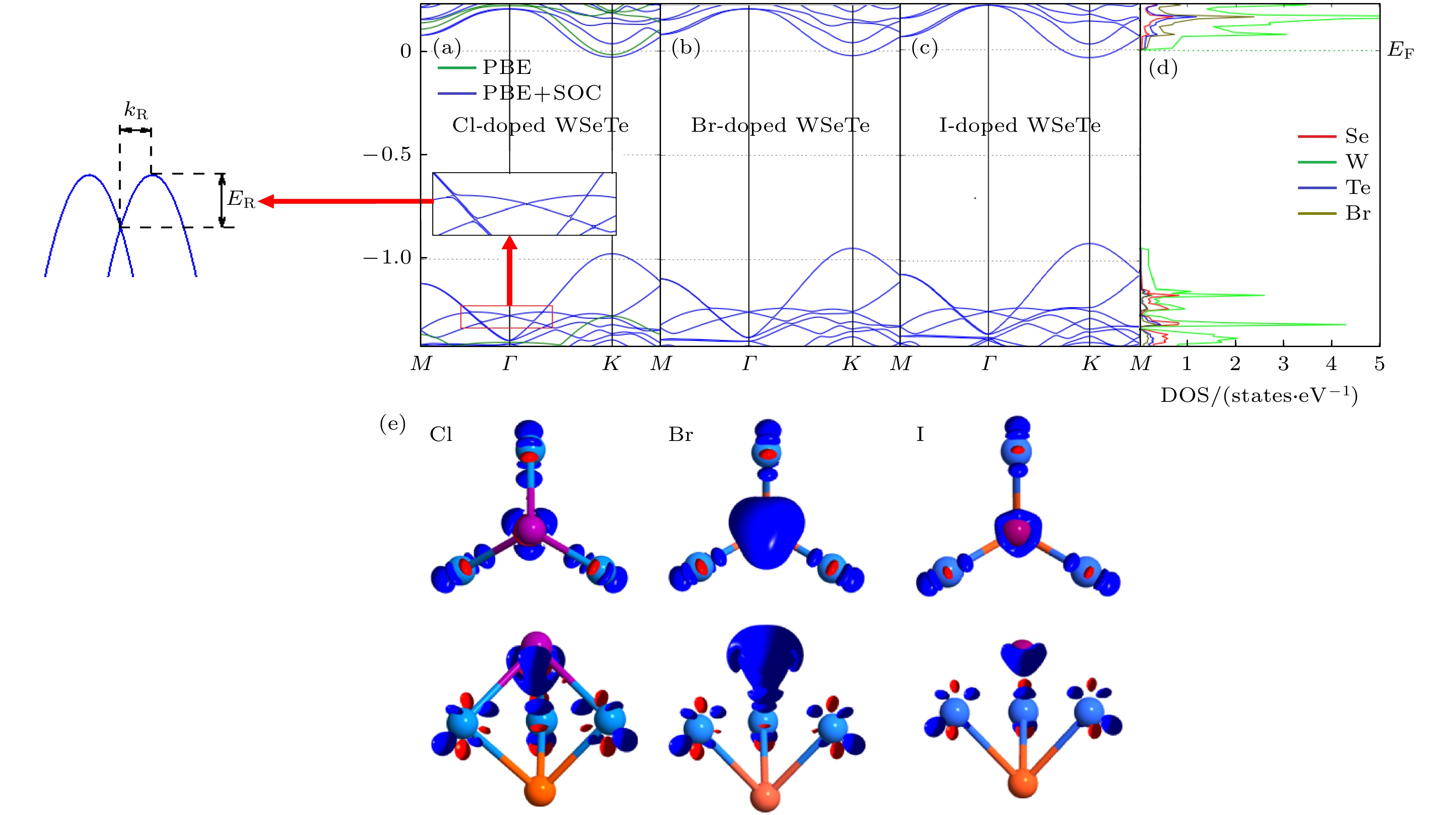 图 2 (a), (b), (c) Cl, Br, I原子掺杂单层WSeTe能带结构图; (d) Br原子掺杂单层WSeTe中单个原子的投影态密度图; (e) VIIA原子掺杂单层WSeTe的差分电荷密度的俯视图(上)和侧视图(下), 红色代表等值面0.01 a.u., 蓝色代表等值面–0.01 a.u.
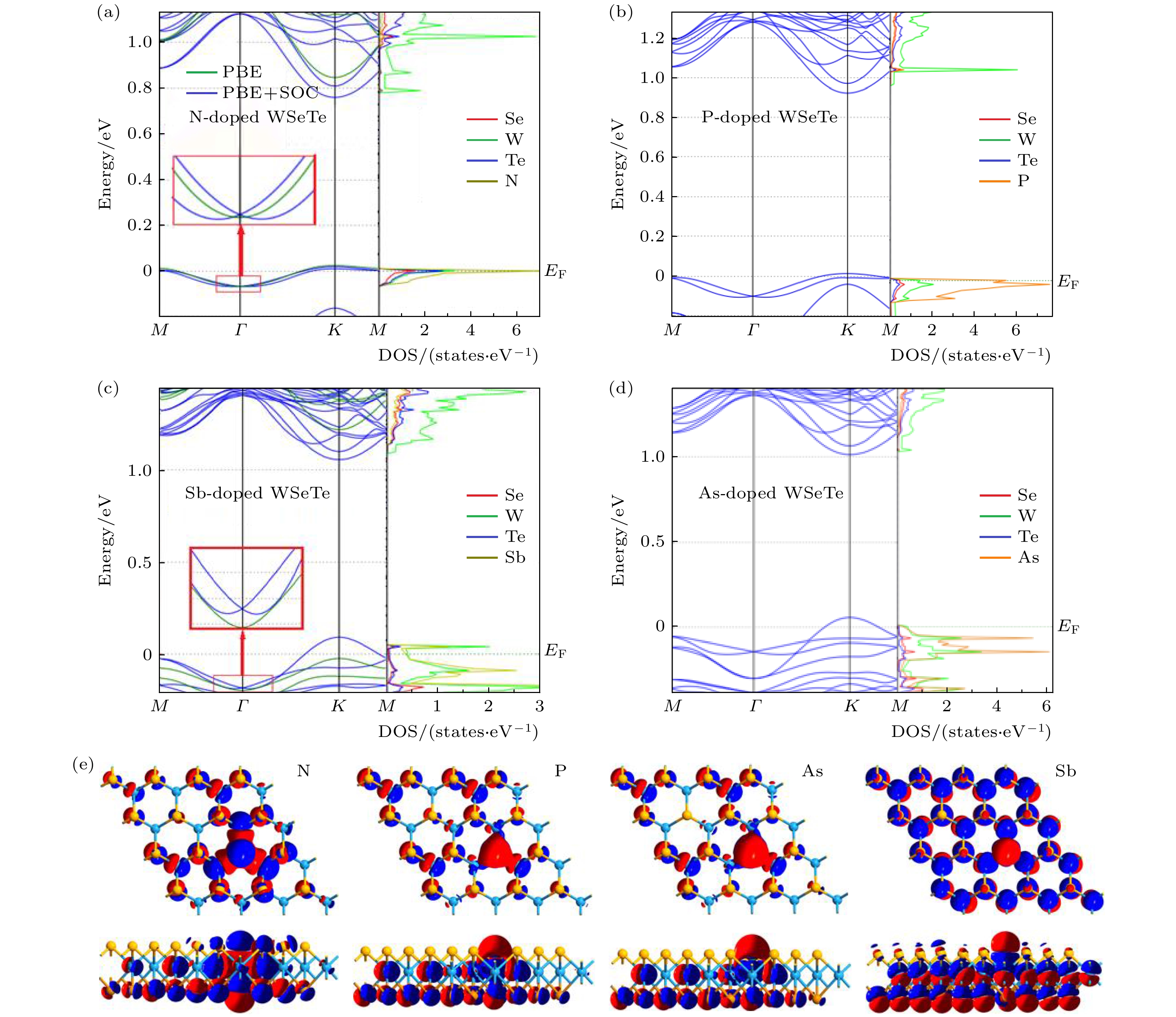 图 3 (a), (b), (c), (d) N, P, Sb, As掺杂单层WSeTe的能带结构图和单个原子的PDOS图; (e) VA原子掺杂单层WSeTe的差分电荷密度的俯视图(上)和侧视图(下), 红色代表等值面0.01 a.u., 蓝色代表等值面–0.01 a.u.


 图 4 3d过渡金属元素掺杂单层WSeTe的能带图, 自旋在z轴方向的期望值


