全文HTML
--> --> -->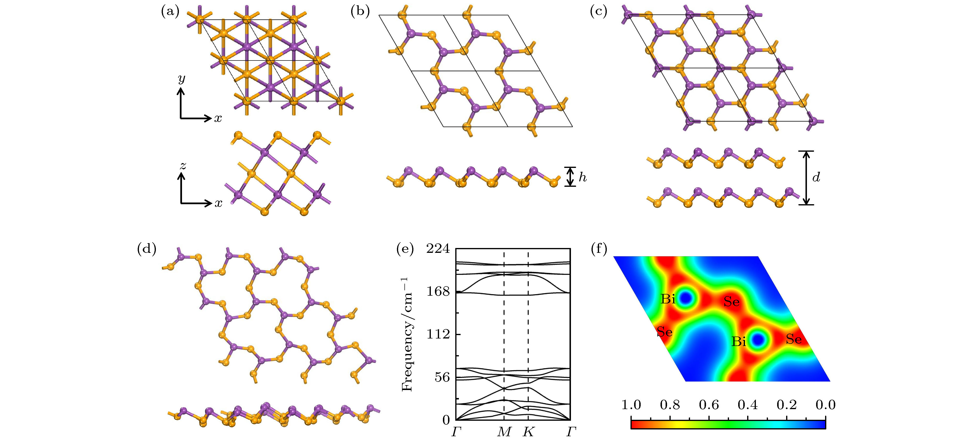 图 1 (a) α-Bi2Se3的原子结构; (b)单层β-Bi2Se3结构的俯视图(上图)和侧视图(下图); (c)双层β-Bi2Se3结构的俯视图(上图)和侧视图(下图); (d)经过10 ps第一性原理分子动力学模拟, 得到了300 K时Bi2Se3单层的平衡结构; (e) β-Bi2Se3的声子谱; (f) β-Bi2Se3单层的电子局域函数
Figure1. (a) Atomic structure of α-Bi2Se3; (b) the top and side views of monolayer β-Bi2Se3; (c) the top and side views of bilayer β-Bi2Se3; (d) snapshots of the equilibrium structures of the β-Bi2Se3 monolayer at 300 K after 10 ps ab initio molecular dynamic simulation; (e) phonon dispersion of monolayer β-Bi2Se3; (f) electron localization function for monolayer β-Bi2Se3.
对于具有特定化学计量比的二维材料, 由于原子杂化方式的不同, 可能存在多种同素异构体, 而异构体的不同原子结构赋予了它们独特的物理和化学性质. 例如石墨烯和石墨炔是二维碳材料的同素异构体: 石墨烯具有sp2杂化的蜂巢结构, 是零带隙半导体, 拥有线性色散关系的狄拉克锥[16]; 石墨炔是由碳的sp和sp2轨道杂化而成, 它具有不同方向变形的狄拉克锥[17]. 黑磷和蓝磷是二维磷烯的同素异构体: 黑磷具有约2 eV的直接带隙和高载流子迁移率等优点[18,19], 可用于可见光范围的光电器件; 蓝磷具有2.73 eV的间接带隙, 在紫外区域吸收较强[20,21], 是紫外探测器件的备选材料. 因此, 探寻新型二维材料可能存在的同素异构体对于研究新奇物理效应、开发具有特定功能的材料体系具有重要推动作用.
本研究首次提出一种新型Bi2Se3同素异形体—β-Bi2Se3. 在密度泛函理论框架下, 采用基于粒子群算法的结构预测方法, 搜索了化学计量比为2∶3的Bi2Se3二维结构, 并进一步计算其稳定性和物理性质. 结果表明, 我们预测的β-Bi2Se3具有良好的动力学稳定性和热稳定性, 它是能隙为2.40 eV的直接半导体, 载流子有效质量低至0.52m0, 在可见光范围内具有高达105 cm–1的光吸收系数, 能带边缘位置适中, 可用于光催化水分解制氢气. 此外, 由于镜面对称性破缺, β-Bi2Se3具有垂直平面的面外压电系数(0.58 pm/V). 因此, β-Bi2Se3在微电子、光电子和压电器件, 以及光催化等领域应用上具有很好的潜力.
为了研究β-Bi2Se3的动力学稳定性, 我们采用基于密度泛函微扰理论(DFPT)和VASP相结合的Phonopy程序计算声子谱[27,28]. 采用以PAW方法和PBE泛函为基础的从头计算分子动力学(AIMD)方法预测Bi2Se3的热稳定性[29]. 在AIMD模拟中, 以3 × 3 × 1的Bi2Se3超胞为初始结构, 模拟了温度为300 K的NVT系综, 总时长为10 ps, 步长为1.0 fs, 温度采用Nosé-Hoover方法控制[30].
采用CALYPSO程序中的粒子群优化(PSO)算法搜索二维(Bi2Se3)n (n = 1—4)单层的结构[31,32], 种群大小和代数都设置为30. 结构搜索的计算使用VASP5.4程序, 基于PBE泛函进行结构弛豫[22].
 图 A1 CALYPSO搜索得到的几个较低能量的Bi2Se3单层结构(a)及对应的声子谱(b), 其中Bi2Se3-1, Bi2Se3-2, Bi2Se3-3的形成能分别为–0.15, –0.12, –0.09 eV/atom
FigureA1. Some typical low-energy structures (a) of freestanding Bi2Se3 monolayer predicted by the CALYPSO code and corresponding phonon dispersions (b). The formation energy of Bi2Se3-1, Bi2Se3-2, Bi2Se3-3 are –0.15, –0.12, –0.09 eV/atom respectively.
 图 A2 温度为300 K时β-Bi2Se3单层的能量-时间变化 曲线
FigureA2. Variations of temperature and energy with the time of AIMD simulation for β-Bi2Se3 monolayer at 300 K.
为了评估β-Bi2Se3的能量稳定性, 我们首先计算了它的形成能, 定义为


 图 2 α-Bi2Se3和β-Bi2Se3体系表面自由能的化学势相图
Figure2. Chemical potential phase diagram of surface free ener-gy for α-Bi2Se3 and β-Bi2Se3.
接着计算β-Bi2Se3单层的电子能带结构和局域态密度(LDOS), 如图3所示. 采用HSE06杂化泛函, β-Bi2Se3在Γ点具有2.66 eV的直接带隙; 考虑自旋轨道耦合效应(SOC)后, 带隙为2.40 eV, 比未考虑SOC减小了约10%, 说明β-Bi2Se3具有较强的SOC. 而考虑SOC情况下单层α-Bi2Se3仅具有0.88 eV的间接带隙, 这个结果与前人的理论计算结果相符合(大约为1.0 eV)[34], 同时实验上所制备的多层α-Bi2Se3带隙随着厚度的增加逐渐减小(0—0.25 eV)[35], 由此推断单层α-Bi2Se3将具有更大的带隙, 与本文计算值定性相符, 说明了我们计算结果的可靠性. LDOS分析表明, β-Bi2Se3价带的边缘主要由Se原子的4p轨道占据, 部分来自Bi原子的6p轨道, 而导带边缘是由Bi原子的6p轨道和Se原子的4p轨道共同贡献. 同时, 在费米能级附近的LDOS的大面积重叠表明: Bi和Se原子的轨道之间具有较强的杂化作用.
 图 3 (a)不考虑SOC和(b)考虑SOC时, 采用HSE06泛函计算得到的β-Bi2Se3的能带结构和LDOS
Figure3. The electronic band structures (left panel) and LDOS (right panel) (a) without and (b) with SOC effect for monolayer β-Bi2Se3 using HSE06 functional, respectively.
由于实验上合成的二维材料薄片可能为多层, 我们还考虑了双层β-Bi2Se3的几种高对称堆叠构型(见附录图A3), 其中图1(c)所示的堆叠方式是最稳定的双层结构, 晶格常数为7.01 ?, 层间距为3.14 ?, 大于Bi—Se键长(2.69 ?), 层间结合能为–0.065 eV/atom, 与石墨烯(–0.065 eV/atom)[36]、磷烯(–0.055 eV/atom)[37]、h-BN(–0.065 eV/atom)[36]的值相近, 说明层间作用为范德瓦耳斯力, 多层或块体β-Bi2Se3不会在层间形成共价键发生重构. 双层β-Bi2Se3的带隙为0.77 eV(见图4). 我们还考察了β-Bi2Se3块体的性质, 其晶格常数为7.00 ?, 层间距为2.37 ?, 考虑SOC计算得到的带隙为0.87 eV, 并且保持了直接带隙的特点. 由此可见, 二维β-Bi2Se3的层厚对电子结构有较大影响: 双层(0.77 eV)和块体(0.87 eV)的带隙很接近, 并且远小于单层的带隙(2.40 eV), 但是体系的厚度并不会影响直接带隙的特点. 电子和空穴的有效质量可以通过拟合导带最小值(CBM)和价带最大值(VBM)附近的二次函数得到. 计算β-Bi2Se3的单层、双层、块体的载流子有效质量范围分别为0.66m0—7.88m0, 0.52m0—2.55m0, 0.63m0—0.67m0(见表1). 值得注意的是, 沿y方向的载流子有效质量可低至0.52m0, 说明载流子在β-Bi2Se3中可能具有较高的迁移率. 而且对于单层和双层β-Bi2Se3, 空穴和电子载流子的有效质量具有很大差异, 将有利于对空穴和电子的筛选, 在太阳能转换方面具有优势. 为了考察应力对能带的影响, 我们进一步计算了单层β-Bi2Se3在双轴应变下的能带结构(见图4(b)), 发现在–3%到3%的应变下, 单层β-Bi2Se3的带隙从2.61 eV线性降低到2.22 eV, 并且依然保持直接带隙的特征.
| β-Bi2Se3 | VBM/eV | CBM/eV | mxh | mxe | myh | mye |
| Monolayer | –5.82 | –3.43 | 7.88 | 0.70 | 5.69 | 0.66 |
| Bilayer | –5.00 | –4.24 | 2.55 | 0.52 | 2.36 | 0.52 |
| Bulk | — | — | 0.65 | 0.63 | 0.65 | 0.67 |
表1单层、双层和块体β-Bi2Se3相对真空能级的价带顶VBM和导带底CBM, 空穴和电子沿着x和y方向的有效质量(mxh, myh, mxe, mye). 载流子有效质量以自由电子的静止质量m0为单位
Table1.The VBM and CBM related to vacuum level for monolayer, bilayer and bulk β-Bi2Se3, and the corresponding carrier effective mass. m0 is the electron rest mass.
 图 4 (a)采用HSE06泛函并且考虑SOC效应的双层(左图)和块体(右图)β-Bi2Se3的能带结构; (b)单层β-Bi2Se3带隙随双轴应变的变化
Figure4. (a) The electronic band structures for bilayer (left panel) and bulk (right panel) β-Bi2Se3 based on HSE06 level with SOC effect; (d) effect of biaxial strain on band gap of monolayer β-Bi2Se3.
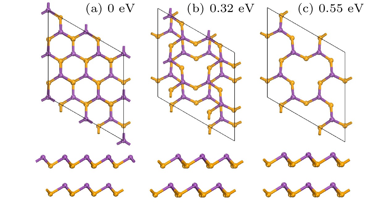 图 A3 不同堆叠方式的双层β-Bi2Se3 (a)能量最低的β-Bi2Se3双层结构, 将它的能量设定为0 eV; (b)相对能量为0.32 eV;(c)相对能量为0.55 eV
FigureA3. β-Bi2Se3 bilayer with different stacking types and their relative energies: (a) the atomic structure of β-Bi2Se3 bilayer with the lowest energy, and its energy is set to 0 eV; the bilayer structures with relative energies of 0.32 eV (b) and 0.55 eV (c), respectively.
接着, 我们探索了β-Bi2Se3用于光催化水分解的可能, 其中一个重要条件是催化剂的带边必须跨越水的氧化还原电势. 对于水分解反应, 标准还原电势为


 图 5 (a)单层β-Bi2Se3的VBM和CBM对比pH = 7和pH = 0的氧化还原电势; (b)单层β-Bi2Se3的光吸收系数, λ是波长, 虚线中间区域表示可见光区
Figure5. (a) The location of VBM and CBM relative to vacuum energy of monolayer β-Bi2Se3 at pH = 0 and 7; (b) optical absorption coefficient for monolayer β-Bi2Se3. λ is the wave length, and the area between the red and the purple represents the visible range
最后, 我们研究了单层β-Bi2Se3的压电性质. 由于单层β-Bi2Se3属于C3V对称点群, 在z方向不具有对称性, 因此β-Bi2Se3具有垂直层面的压电效应. 为了计算β-Bi2Se3的压电系数, 我们采用Duerloo等[43]发展的方法估算不同单轴应变下的弹性常数和极性的变化. 面内的弹性常数可以通过下列公式得到:
感谢内布拉斯加大学林肯分校化学系Zeng Xiao Cheng教授的讨论.
附录
