全文HTML
--> --> -->随着光电信息技术的快速发展, 光电探测器已经成为日常生活中不可或缺的一部分, 包括环境监控、光通信、热成像及军事化应用[7,19]等. 常规的硅基光电探测器[20,21]在可见到近红外波段占据了当前光电探测器的主导地位, 但是硅基光电探测器的应用也存在着一些限制. 随着硅基半导体的制造技术接近“摩尔定律”的极限, 器件尺寸进一步缩小时, 经典物理理论将不再适用; 硅基探测器对光的吸收率不高和吸收光谱窄也限制了它的广泛应用, 此外硅基光电探测器也难以在柔性器件中[22,23] 应用. 当前对光吸收效率高、宽频谱及柔韧性好的新材料的需求日益增长, 以及对二维材料硏究的不断深入, 这些新颖的二维材料为高性能光电探测器的设计和制备提供了新的机遇, 弥补硅基探测器应用上的一些限制. 二维光电探测器[14,24]技术的突破有望实现柔性化、高性能、宽频谱探测, 在未来光电探测器的应用上有很好的前景.
在本文中, 我们首先介绍光电探测器性能参数指标和光栅局域调控的工作原理; 进而总结了基于光栅效应的二维材料及范德瓦耳斯力异质结的光电探测器应用; 最后对光栅局域调控二维探测器未来的挑战进行简要的总结和展望, 并对光栅局域调控探测器提出了新的结构.
2
2.1.光电探测器主要性能参数
一般来说, 可以采用一些参数评价光电探测器的性能, 下面将简要介绍这些参数.光响应度(R)[34]指光电流或光生电压与入射光功率之比. 表达式为


光增益(G )[35]揭示探测器灵敏度的重要指标, 指单位时间内收集的载流子与吸收光子之比. 具体计算公式为

噪声等效功率(noise equivalent power, NEP)[36]是指带宽为1 Hz时, 信噪比达到1所需的最小入射光功率, 公式表示为

探测率(D*)[37]用于判断的不同结构的光电探测器性能的重要参数, 排除了器件面积和带宽的影响, 用公式表示为


响应时间(τ)[38]是光电探测器的重要工作参数之一. 其中上升时间(


2
2.2.光栅局域调控工作原理
光栅效应是指在光照作用下, 吸收光子产生的电子或空穴处于陷阱态, 电荷陷阱态作为局域光栅对导电沟道进行调制的现象, 如图1(a)所示[39]. 图 1 光栅效应特性 (a) 光栅效应示意图[39]; (b) 光照后, 转移特性曲线
Figure1. The characteristics of the photogating effect: (a) Schematic diagram of the photogating effect[39]; (b) the

光栅效应是光电导效应的一种特殊情况, 也表现为在光照下电导率的改变. 光激发会产生两种载流子, 其中一种载流子会被陷阱捕获, 另一种载流子在导电沟道中进行传输, 被陷阱状态捕获的载流子这时可看作为局部光栅, 来调制沟道的电导率[40]. 若 陷阱捕获空穴带正电, 则转移特性曲线左移; 若陷阱捕获电子带负电, 则转移特性曲线右移, 如图1(b)所示. 因此, 基于光栅效应光电探测器产生的光电流可能小于暗电流, 也可能大于暗电流. 根据已报道的文献, 形成


基于光栅效应的光电探测器产生的光电流可能小于暗电流, 会出现负电导(negative photoconductance, NPC)[41,42], 如图1(b)所示, 光照后, 转移特性曲线向正方向移动, 表明由捕获电子引起负栅压(


图1(b)中的


NPC是指在光照的条件下材料的电导下降的现象[43]. 由于NPC需要多数载流子和多数载流子陷阱状态的共存, 导致NPC更有可能在异质结结构中被发现, 而不是在单一材料二维探测器中. 通常, 大多数载流子陷阱状态在光照之前已被大多数载流子填充, 使其难以产生明显的光电压, 异质结构中的NPC现象也成为了光栅效应的有力证据[44].
2
3.1.石墨烯光电探测器
Liu等[6]设计出超带宽的石墨烯光电探测器, 由两层石墨烯夹着薄隧道势垒组成, 如图2(a)所示. 与常规的光电晶体管及横向石墨烯器件[53,54]相比, 光生载流子会隧穿进入底层石墨烯, 减少了载流子的复合. 因此, 顶部石墨烯积累了大量载流子, 导致较强的光栅效应, 对底部石墨烯沟道层进行调控. 利用这种结构, 实现了从可见光到中红外光的探测范围, 器件光响应度超过1000 A/W. 通过改变隧穿层的材料, 还可以进一步提高光响应度. 现有光电探测器器件受到光栅效应的限制, 实现超高光响应度的同时牺牲了响应时间. 为解决光栅效应中响应时间慢的问题, Guo等[55]采用石墨烯/SiO2/轻掺杂Si结构, 如图2(b)所示, 利用界面栅控机制来平衡超快响应和超高响应度之间的差距. SiO2/Si之间存在正电荷局部界面态, 并在界面附近的硅中感应出负耗尽层, 并形成内建电场. 光照时, 在内建电场作用下, 轻掺杂Si中的光生电子空穴对被分离, 电子聚集在SiO2/Si界面处形成负栅压对石墨烯导电沟道进行调控. 利用这个原理, 器件能够检测 < 1 nW的信号, 响应度高达1000 A/W, 光响应时间缩短为400 ns, 并且光谱响应范围从可见光扩展到近红外. 这项工作为基于石墨烯的高性能光电器件开辟道路, 而且在超快微弱信号检测方面也具有巨大潜力. 图 2 单一二维材料光电探测器 (a) 双层石墨烯异质结中的光激发热载流子隧穿[6]; (b) p型轻掺杂Si/SiO2衬底上的石墨烯光电探测器的示意图[55]; (c) p型InSb衬底上石墨烯场效应晶体管的示意图[59]; (d) 电荷陷阱模型和简化的能带图[40]; (e) 光响应度与顶栅Vtg的关系[65]; (f) 不同衬底下的光响应度[58]; (g) 在不同入射功率下, 在最大跨导附近实现最大光电流[35]; (h) 光电流与时间的关系[67].
Figure2. Single two-dimensional material photodetector: (a) Photoexcited hot carrier tunnelling in graphene double-layer heterostructures[6]; (b) schematic diagram of the graphene photodetector on lightly p-doped silicon/SiO2 substrate[55]; (c) schematic diagram of the InSb-based graphene field effect transistor (FET)[59]; (d) charge trapping model and simplified energy band diagram[40]; (e) the relationship between photoresponsivity and Vtg[65]; (f) photoresponsivity under different substrates[58]; (g) the maximum photocurrent is realized near the maximum transconductance at different incident power[35]; (h) the relationship between photocurrent and time[67].
为了进一步提高石墨烯探测器响应度, Howell等[56]提出了一种基于深耗尽的石墨烯-绝缘体-半导体的光电探测器. 器件绝缘体层选用50 nm HfO2, 由于HfO2层的介电常数大[57], 能削弱载流子间的库仑相互作用, 因此减少了载流子散射, 提高了迁移率. 深耗尽的低掺杂硅衬底内产生的光生载流子聚集在半导体/绝缘体界面形成的势阱中, 产生光生栅压对石墨烯场效应晶体管进行调控, 增加导电沟道浓度. 由此产生的器件在可见光波长范围内显示出高达2500 A/W响应度. 改变器件衬底也是提升器件性能的方法[58], Fukushima等[59]利用光栅效应制造了基于锑化铟(InSb)衬底的中波长红外(MWIR)波长的高响应性石墨烯光电探测器, 如图2(c)所示. 利用InSb响应入射的红外光而生成的光载流子, 产生光生栅压, 调制了石墨烯导电沟道, 并感应出大的光电流. 在50 K时实现了33.8 A/W的超高响应度, 为提高光响应度提供了新的思路. Cao等[60]设计出混合InGaAs-SiO2-石墨烯光电探测器, 此探测器将窄带隙InGaAs作为光吸收层, 石墨烯作为透明的沟道传输层. 对比于InGaAs PIN光电二极管, 混合结构光电探测器表现出了从紫外到近红外波段的宽频谱响应, 在弱光照下, 光响应度高达103 A/W, 响应时间提高到了微秒级别.
2
3.2.其他光电探测器
除了石墨烯光电探测器外, TMDs作为典型的二维材料, 具有较大的带隙和适中的载流子迁移率, 适合在电子/光电子器件方面的研究. 其中, MoS2光电探测器在性能方面就表现优异[40,61-63].Furchi等[40]研究了MoS2中的光电导机理时, 确认了光栅效应和光电导效应是并存. MoS2/SiO2界面处或附近分子的光生载流子充当额外的栅极电压并导致转移曲线漂移. 同时, 带尾态捕获的多余载流子有助于形成局域光栅, 如图2(d)所示. 与光电导相比, 光栅效应的光电流分量幅度较大, 但速度较慢. 同样的现象也被Kufer等[63]发现, 通过控制栅极电压, 可以将MoS2器件的响应度和时间响应上调几个数量级. 当施加强负

除了MoS2之外, 还有很多其他二维材料例如BP和ReS2等也在光电器件中使用光栅效应来加强光响应度. Guo等[17]利用光栅效应实现了具有高增益的MIR BP光电探测器. 光电探测器的光电流在阈值电压附近的最大跨导点处达到峰值, 这与公式Iph = gmΔVg 一致, 如图2(g)所示, 也意味着这是光栅效应主要的位置. 实验表明在3.39 μm波长下, 探测器具有很高的内部增益, 光响应度达到82 A/W. Thakar等[67]制作了两种ReS2光电探测器, 一种ReS2和SiO2衬底直接接触, 另一种ReS2悬空在SiO2衬底上. 他们对直接接触和悬空的ReS2光电晶体管的响应速度和响应速度的体系结构, 激光功率和栅极偏置依赖性进行了全面研究. 尽管悬空会导致栅极调控能力的削弱, 但界面缺陷的减少使之能达到和前者相同的响应速度. 通过栅极电压的调节, 两种结构的器件的光响应度均能达到约4 A/W, 响应时间最短能达到20 μs, 如图2(h)所示, 是目前为止速度最快的光电探测器.
4.1.与石墨烯构成的异质结
自从2004年石墨烯被发现以来, 多种二维材料不断被发现, 研究人员对二维材料的研究也不断深入, 这些新颖的二维材料为高性能光电器件的设计和制备提供了新的机遇, 特别在光电探测器方面[68]. 在室温下, 石墨烯的光电响应波段可以到中波红外[69-71]乃至到太赫兹波段[72], 其具有超高的载流子迁移率, 超过15000 cm2·V–1·s–1[73]可用于制作超快响应速度的射频器件. 但是石墨烯作为光电探测器, 受到厚度的限制, 对光的吸收不高, 因此光响应率一直都不是很高, 在几到几十A/W的量级[74-76]. 另外石墨烯的零带隙和高导电率, 使得暗电流较大, 探测率也会大大降低. 在如何充分利用石墨烯迁移率高、吸收波段宽等优势, 而又解决石墨烯探测器光响应度不高、暗电流大等劣势, 利用光栅局域调控在解决这些问题上起着很大作用.光增益

| Material | Responsivity/(A·W–1) | Gain | Response time/ms | Detection range/nm | Ref. |
| Gr/MoSe2 | 1.3 × 10⁴ | — | 22000.0 | 550 | [83] |
| Gr/MoTe2 | 970.82 | 4.69 × 10⁸ | 78.0 | 1064 | [86] |
| Gr/ReS2 | 7 × 10⁵ | — | 30.0 | 550 nm | [85] |
| Gr/WS2 | 950 | — | — | 340–680 nm | [84] |
| Gr/MoS2 | 107 | 108 | — | 650 | [87] |
| Gr/BP | 55.75 | — | 36.0 | 655 | [82] |
| Gr/BiI3 | 6 × 10⁶ | — | 8.0 | 532 | [88] |
| Gr/PbSe | 6613 | 7824 | 25.0 | — | [16] |
| Gr/Bi2Te3 | 35 | 83 | 8.7 | 532—1550 | [78] |
| Gr/MoS2 | 5 × 10⁸ | — | — | 635 | [77] |
| Gr/Bi2Se3 | 8.18 | — | — | near-IR 750—2500 | [38] |
表1基于石墨烯异质结(Gr)的光栅局域调控光电探测器
Table1.Graphene(Gr)-based photodetectors with grating photogating.
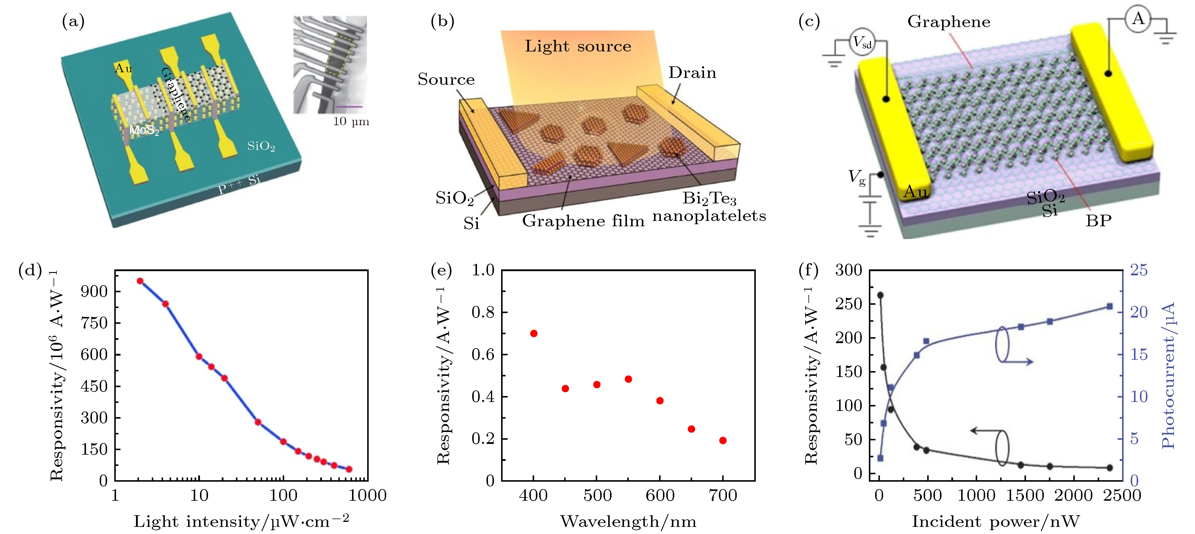 图 3 石墨烯异质结光电探测器: (a) 石墨烯/ MoS2异质结光电探测器的示意图; (b) 石墨烯/Bi2Te3异质结光电探测器的示意图; (c) 石墨烯/BP异质结光电探测器的示意图; (d)光响应度与光照强度的关系; (e)光响应度与波长的关系(VD = –3 V, VG = –30 V); (f)在波长为980 nm, 光电流和光响应随入射光强的关系 (VDS = 1 V, VG = 0 V).
Figure3. The photodetectors based on graphene heterostructures: (a) Schematic of device architecture graphene/MoS2 photodetector[77]; (b) schematic of the heterostructure phototransistor device[78]; (c) graphene/BP heterostructure photodetector[82]; (d) the relationship between photoresponsivity and light intensity[89]; (e) responsivity as a function of the wavelength (VD = –3 V, VG = –30 V)[85]; (f) photocurrent and photoresponsivity versus incident light power at 980 nm. (VDS = 1 V, VG = 0 V)[86].
2
4.2.不同二维材料构成的异质结
4.1节主要介绍了基于石墨烯的异质结光电探测器, 接下来将讨论其他非石墨烯异质结的光电性能. 利用pn异质结构成的强烈内建电场可有效地分离光生电子空穴, 缩短响应时间的同时, 还可以用静电作用调控载流子的浓度及能带结构来提高光电探测器的性能.Qi等[89]采用两次CVD生长的方法实现了超快响应、性能稳定的PbI2/WS2红外波长的光电探测器, 如图4(a)所示, 其中顶层的PbI2既为封装层也为载流子传输层, WS2作为光栅层来调节载流子浓度. 由于pn异质结中的强烈的内建电场, 加速了光激发电子-空穴对的分离和抑制了光生载流子的复合, 从而导致高达5.57 × 10² A/W的光响应性, 上升时间和衰减时间也分别只有24 ms和33 ms, 如图4(b)所示. 其中, 光响应度是其他气相生长垂直pn异质结构中的最高值, 与单纯PbI2相比, PbI2/WS2异质结光电探测器的光响应性提高了3个数量级. 此外, 在施加–60 V的栅极电压偏置时, 可将其进一步提高至7.1 × 10⁴ A/W; 在栅极电压为–40 V时, 探测率超过4.9 × 10¹³ Jones. Yang等[90]利用CVD制备了毫米级大尺寸WSe2/SnS2纵向双层异质结, 如图4(c)所示. Krause等[91]用第一性原理计算出的双层WSe2/SnS2异质结构的相对能带排列. 由于异质结中WSe2的价带高于SnS2的导带, 形成了Ⅲ型断裂能带结构[92], 如图4(d)所示, 抑制了光生载流子的复合, 从而提高了光响应度. 他们利用多电极的背栅场效应晶体管, 测出3种不同工作模式: 纯WSe2晶体管、WSe2/SnS2串联晶体管及WSe2/SnS2并联晶体管. 其中, 串联模式WSe2/SnS2 pn结具有极低的漏电流, 只有10–14 A, 开关比高达107. 在光电方面, 串联模式WSe2/SnS2异质结光响应性为108.7 mA/W, 探测率为4.71 × 10¹⁰ Jones和响应速度为500 μs. 相较于文献所报道的CVD生长的纵向异质结探测器, 其光电性能有了一定的提升, 甚至优于部分机械剥离堆叠而成的异质结光电探测器. Ye等[93]以BP为光敏层、WSe2为沟道层, 制备出了纵向光栅结构的BP/WSe2的高带宽光电探测器, 如图4(e)所示. 在光激发条件下, BP和WSe2都可以产生光生载流子, 内建电场促使BP中的光生电子转移到WSe2中, 导致沟道材料WSe2中更多的电子被收集从而形成更大的光电流. 而WSe2中的光生空穴被内建电场转移到BP中并留在BP, 作为光栅对沟道进行调制. 室温下可见光和红外光响应率分别可以达到103和5 × 10⁻¹ A/W, 探测率分别高达1014和1010 Jones, 如图4(f)所示. 器件利用BP具有各向异性[10]特点, 测得器件在1550 nm波长下偏振依赖光响应度最大约40 mA/W, 其入射光沿水平轴偏振(定义为0°); 最小响应度约68 mA/W, 其偏振方向沿竖直方向(定义为90°), 器件表现为比较敏感的极化红外光照探测. Guo等[94]提出一种新结构, 通过引入陷阱层来提高增益, 实现了超高的光响应度, 如图4(g)所示. 光照时, p型WSe2纳米片作为光敏栅极提供外部电压对ZnO导电沟道内的耗尽区域进行调制, 如图4(h)所示. 其中, 光电探测器的增益和响应时间分别由场效应调制和光驱动晶体管的转换速度确定, 利用此机制光电探测器的光响应度和增益分别达到4.83 × 10³ A/W和104, 同时, 也得到了较快的响应时间为10 μs, 如图4(i)所示.
 图 4 基于光栅效应的PN异质结光电探测器 (a) PbI2/WS2异质结构光电探测器; (b) PbI2/WS2光电探测器的光响应时间[89]; (c) WSe2 /SnS2多电极异质结构背栅器件的示意图; (d) WSe2/SnS2异质结的能带结构和光激发、层间弛豫过程的示意图[90]; (e)基于光栅效应的WSe2/BP光电探测器示意图; (f) 在1 mW/cm2的入射功率密度和0.5 V偏置下, 光增益G和探测率D对不同波长照明的依赖关系[93]; (g) 在637 nm光照下器件的示意图; (h)顶栅电极侧面和重叠区域之间形成导电通道Vtg; (i)一个调制周期: 上升时间为10 μs、下降时间为10 μs的快速分量和20 μs的慢速分量组成[94].
Figure4. PN heterojunction photodetector based on photogating effect: (a) Schematic device structure of PbI2/WS2 photodetector fabricated on SiO2/Si substrate; (b) time-resolved photoresponse of PbI2/WS2 phototransistors[89]; (c) schematic diagram of the multi-electrode WSe2/SnS2 vdW heterostructure backgate device; (d) schematic diagram of WSe2/SnS2 heterostructure band structure and photoexcitation, interlayer relaxation process in WSe2/SnS2 heterojunction[90]; (e) schematic illustration of the BP on WSe2 photodetector with photogate structure; (f) the dependence of the photogain


为了解决以上问题, 未来可在以下方面进行探究: 优化材料的合成方式, 实现能规模化制备的方法; 改善器件结构, 可将石墨烯和pn异质结结合起来, 利用石墨烯的高迁移率获得高增益和高响应度, 同时pn结中的内建电场加速电子空穴对的分离与复合提高响应速度, 如图5所示, 进一步去提高二维光电探测器的性能. 总的来说, 光栅局域调控在改善二维光电探测器性能有着优异的表现, 在未来光电探测器应用上有着巨大潜力.
 图 5 基于光栅效应的光电探测器新结构 (a)器件结构示意图; (b)器件结构能带图
Figure5. New structure of photodetector based on photogating effect: (a) Schematic diagram of device structure; (b) sche-matic diagram of energy band structure
