Key Laboratory of Advanced Semiconductor Devices and Materials, School of Electronic Engineering, Xi’an University of Posts & Telecommunications, Xi’an 710121, China
Fund Project:Project supported by the National Natural Science Foundation of China (Grant No. 61306131) and the Natural Science Basic Research Program of Shaanxi Province, China (Grant No. 2020JM-581)
Received Date:01 April 2020
Accepted Date:15 May 2020
Available Online:25 May 2020
Published Online:20 August 2020
Abstract:Gallium oxide (Ga2O3) single crystal nanoribbons have the potential applications in electronic devices due to their unique properties. However, the current small surface area makes the fabrication of device based on this nano-material very complex and challenging, and the introduction of catalyst also makes the growth process of Ga2O3 nanomaterial complicated and hard to control. Therefore, it is very important to study the growth method and physical mechanism of Ga2O3 nanoribbon with the larger surface area without catalyst. In this paper, the carbothermal reduction method is used to grow the Ga2O3 nanomaterial. In this paper, the gallium oxide powder mixes with the carbon nanotubes at a mass ratio of 1:1.5 without the catalyst, and then they are put into a high temperature diffusion furnace for the growth of Ga2O3 nanomaterials with different structures on silicon-based substrates by controlling the reaction temperature. In this paper, it is found that the reaction temperature directly affects the diameter and ratio of gallium oxide nanostructures. The reason is that the bonding energy of gallium oxide crystal is different in different crystal directions which leads to the different growth speed. The interface energy along the growth direction is the smallest and the growth speed is the fastest, while the growth speed along the vertical direction is slow. Finally, the crystal gradually grows into nanoriband, nanometer sheet and other structures. In addition, the ultra-wide β-Ga2O3 single crystal nanobelt up to the millimeter level was prepared in this paper. This nanobelt’s lateral dimension is observed to reach 44.3 μm under the scanning electron microscope (SEM), and the transmission electron microscope (TEM) is used to confirm that the nanoribbons have a single crystal structure. Further, Raman spectroscopy (Raman) shows that the β-Ga2O3 nanoribbons grown by this method have the smaller strain and the lower defect density. Additionally, the room temperature photoluminescence spectrum (PL) test shows that the gallium oxide nanoribbon emits a stable and high-brightness blue light at 425 nm at the excitation wavelength of 295 nm. This growth method can provide a useful way for the preparation of device-level gallium oxide nanoribbons in the future. Keywords:β-Ga2O3/ carbothermal reduction/ crystal nanoribbons/ defect density
图2进一步给出氧化镓纳米带更加精细的表面形貌结构. 图2(a)为样品C在中低倍镜下的特征, 可以观察到合成的氧化镓纳米带的长度达到2—3 mm. 图2(b)中, 在高倍镜下可以清楚观察到样品C的横向尺寸已经超过44.3 μm, 整体呈膜状结构. 同时, 图2(c)显示样品C的纳米带相互缠结并弯曲, 证明其有良好的可塑性, 可以承受较大的变形. 图2(d)为样品D, 高倍镜下可以观察到在950 ℃下纳米带尺寸未有明显提高, 但表面凝结大量块状结构, 样品形貌受温度影响强烈, 此时形貌已经开始恶化, 已不再适宜于生长. 基于上述结果, 氧化镓纳米带最佳生长温度应为900 ℃, 在此温度下可以产生大量表面形貌均匀且稳定的超长氧化镓纳米带. 图 2 (a) 低倍镜下样品C超长的氧化镓纳米带; (b) 样品C高倍率下单个氧化镓纳米带; (c)互相缠绕弯曲的纳米带; (d) 高倍镜下样品D纳米带表面结块恶化 Figure2. (a) The ultra-long gallium oxide nanoribbons of sample C under low magnification; (b) single gallium oxide nanoribbon at high magnification of sample C; (c) intertwined curved nanoribbons; (d) under high power, the agglomeration of the surface of the sample D nanoribbons deteriorates.

 图 1 样品A—D在不同生长温度下的SEM图像 (a) 样品A (800 ℃); (b) 样品B (850 ℃); (c) 样品C (900 ℃); (d) 样品D (950 ℃)
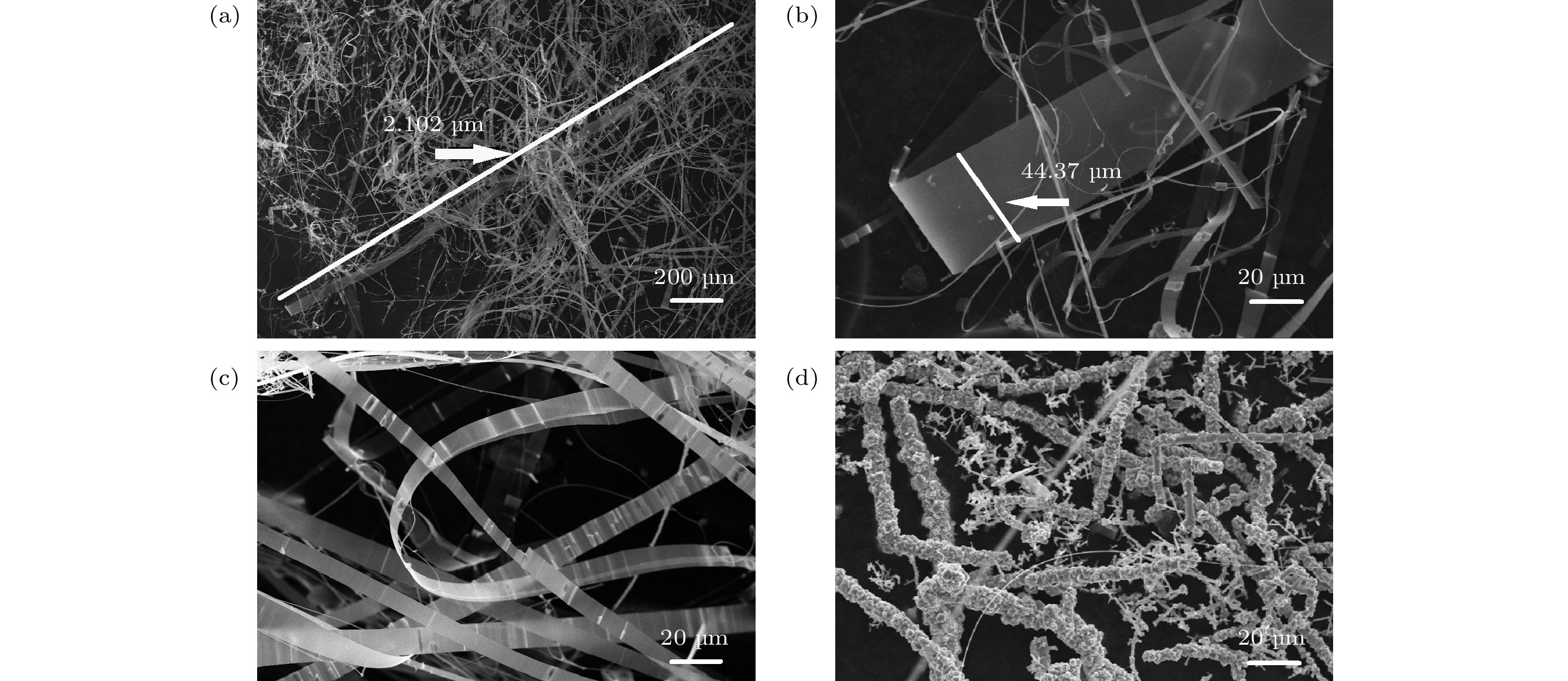 图 2 (a) 低倍镜下样品C超长的氧化镓纳米带; (b) 样品C高倍率下单个氧化镓纳米带; (c)互相缠绕弯曲的纳米带; (d) 高倍镜下样品D纳米带表面结块恶化
 图 3 (a)样品C的X射线衍射图; (b)样品C的拉曼光谱
 图 4 (a) 样品C的TEM图像, 插图显示了SAED模式; (b) 样品C的HR-TEM图像
 图 5 β-Ga2O3纳米带的室温PL光谱