全文HTML
--> --> -->光谱椭偏仪是一种典型的光学散射仪, 其基本测量原理是通过将实际测量数据与模型仿真数据进行匹配来反演出待测纳米结构参数值[11]. 其中, 测量数据由椭偏仪探测待测纳米结构的反射光或透射光而直接获得, 根据测量数据类型的不同, 测量仪器又可分为传统椭偏仪和Mueller矩阵偏振仪; 模型仿真数据的计算和待测参数值的反演提取则涉及到以下两个光学散射测量理论算法: 一是“正向”光学特性的建模; 二是“逆向”待测参数的提取. 正向光学建模是由已知的纳米结构参数、材料光学常数以及测量条件配置等, 利用电磁场理论计算出待测结构的理论数据[12]; 逆向几何参数求取则是将实际测量数据与模型计算数据进行匹配反演得出待测参数值[13]. 在以计算电磁波理论为基础的光学特性建模求解方法[12,14,15]中, 由于严格耦合波分析(rigorous coupled-wave analysis, RCWA)可对任意周期性结构建模, 而且具有数值求解过程比较简单、实现相对容易、精度高等优点而得到了广泛应用[16,17]. 纳米结构待测参数的逆向求解主要包括库匹配和非线性回归这两种方法[18], 由于前者的建库过程相当耗时, 后者的操作过程简单直接, 因而具有迭代收敛快速特点的列文伯格-麦夸特(Levenberg-Marquardt, LM)非线性回归优化算法目前被广泛应用于光学散射测量中的待测参数逆向求解[19,20].
在纳米结构三维几何形貌的逆向提取过程中, 为了降低待测参数之间的耦合性, 通常需要将已知的纳米结构参数、材料光学常数、入射测量条件配置等设为固定值, 而对待测的若干形貌参数进行浮动处理[6-10]. 考虑到纳米结构测量数据的质量完全取决于测量仪器本身, 无法轻易改变, 目前已有诸多文献通过优化入射测量条件配置以提高待测参数的测量精确度. 例如, Vagos等[21]基于不确定度与灵敏度分析进行了光学特性模型及方位角的优化; Littau等[22]针对采用不同方式进行入射角范围的选取, 从而提高了角分辨型椭偏仪的测量精度; 文献[23, 24]中分析了不同来源的系统误差对纳米结构参数测量准确度的影响, 进而优化了测量入射角和方位角; 此外, 文献[25]中还结合全局灵敏度分析方法实现了测量方位角的优化, 提高了纳米结构形貌参数的测量精度.
总体而言, 上述优化方法均是通过合理地选择测量条件配置, 以降低测量随机噪声或者系统误差对纳米结构待测参数逆向提取结果的影响, 进而在一定程度上提高测量准确度或精密度. 结构的材料光学常数获取方式通常为测量同一工艺中尚未制作出形貌结构的薄膜培片, 而后在纳米结构三维形貌参数的光学散射测量过程中使用测得的光学常数并假设其固定不变. 这一假设对于半导体制造工业中的绝大多数材料是成立的, 但某些感光材料诸如聚甲基丙烯酸甲酯(polymethyl methacrylate, PMMA)光刻胶[26,27]可能会随着椭偏仪入射光照射的影响而发生改变, 该误差则可能在一定程度上传递给待测形貌参数的逆向提取值. 为此, 本文结合实验与仿真开展了椭偏仪入射光照对PMMA光刻胶薄膜培片和光栅结构的光学散射测量研究, 以证明PMMA光刻胶光学常数随入射光照的变化对于纳米结构的光学散射测量不容忽视, 从而为更进一步提高光刻胶纳米结构三维形貌参数的测量精确度提供理论依据.
2.1.基于RCWA的正向光学特性建模
利用RCWA理论对周期性光栅结构进行光学特性建模的基本步骤可分为: 1)由Maxwell方程组求得入射区域和透射区域的电磁场的表达式; 2)对光栅区域内的介电常数及电磁场按Fourier级数展开, 并由Maxwell方程导出耦合微分方程组; 3)分别在光栅区域的上下边界运用电磁场边界连续条件, 通过数学求解各级衍射波的振幅, 进而计算各级衍射波的衍射效率或衍射场的强度分布等.以图1所示的光栅结构为例, 假设其周期为P, 占空比为f, 线高为d, 顶部线宽和底部线宽分别为DTC和DBC, 首先建立如图1(a)所示的直角坐标系, θ为入射角, 入射波波矢k1所在的铅垂面与xoz平面夹角为方位角φ, 电矢量E与k1所在平面的夹角为偏振角ψ. 然后, 将光栅截面进行纵向分层, 则可将图1(b)中的每个薄层等效为矩形光栅, 再将矩形光栅结构划分为3个区域, 即区域1 (入射/反射区域, z < 0), 区域2 (透射区域, z > d)以及光栅区域(0 < z < d). 区域1和区域2的复折射率分别记为n 1和n 2. 光栅区域包含了脊部和槽部两种介质的周期分布, 分别记其复折射率为n rd和n gr. 由于本文所研究对象的材料为各向同性材料, 因此光栅区域的相对介电常数ε仅为关于x的周期性函数, 而与z无关. 将光栅区域的相对介电常数展开成Fourier级数形式, 有
 图 1 (a) 线条光栅结构的几何形貌示意图; (b) RCWA建模的分层示意图
Figure1. (a) Geometry of the trapezoidal groove line grating; (b) layers division for inverse modeling based on RCWA.
将入射电场的振幅归一化后, 入射波的电场分量可表示成:
由Rayleigh展开可分别得到区域1 (z < 0)和区域2 (z > d)电场矢量的表达式:


由Maxwell旋度方程, Eg与Hg有如下的耦合关系:
考虑到仪器探测设备主要检测的是光强信息, 基于RCWA模型输出的相应为反射率、椭偏参数或Mueller矩阵等光学特性参量的计算值. 其中, 反射率的计算公式为
由偏振光学可知, 待测样品的光学特性则可以用2 × 2阶Jones矩阵J或者4 × 4阶Mueller矩阵M来表征. 例如, 对应于待测样品的Jones矩阵J有


2
2.2.基于LM局部优化算法的待测参数逆向求解
对于光学散射测量中的逆问题, 采用非线性回归法中的LM局部搜索算法对纳米结构的待测参数进行逆向求取, 该算法结合了梯度下降法和高斯-牛顿法, 是一种采用标准数值优化的快速算法[29]. 不失一般性, 在参数提取过程中, 利用S维列向量表示一组需依据评价函数值的大小进行浮动变化的参数, 并记为x = [x1, x2, ···, xS]T, 其中x1, x2, ···, xS可以表示光栅结构的顶部线宽、线高及侧壁角等待测参数; 将固定不变的参数组成的L维列向量记为a = [a1, a2, ···, aL]T, 其中a1, a2, ···, aL可以是测量条件、材料的光学常数, 还可以是纳米结构的已知测量值的几何特征参数, 如薄膜厚度等; 数据拟合时, 采用χ2形式的评价函数来衡量测量和计算得到的椭偏参数或者Mueller矩阵元素之间的拟合误差.以Mueller矩阵元素为例, 其测量值


为了方便起见, 将测量得到的Mueller矩阵元素


对于(16)式描述的逆问题, 本文利用LM优化算法提取待测参数的流程为: 首先设置一组迭代参数初值x0, 然后利用所建正向光学特性模型计算出待测纳米结构对应的理论光谱, 通过定义某种评价函数来进行理论计算光谱与测量光谱的比对, 若评价函数值大于其预设的精度值, 则根据一定准则修改当前参数值, 重复上述过程, 直到评价函数值小于预设的精度值时则认为实现了理论计算光谱与测量光谱的最佳拟合, 即可得到待测参数的输出结果

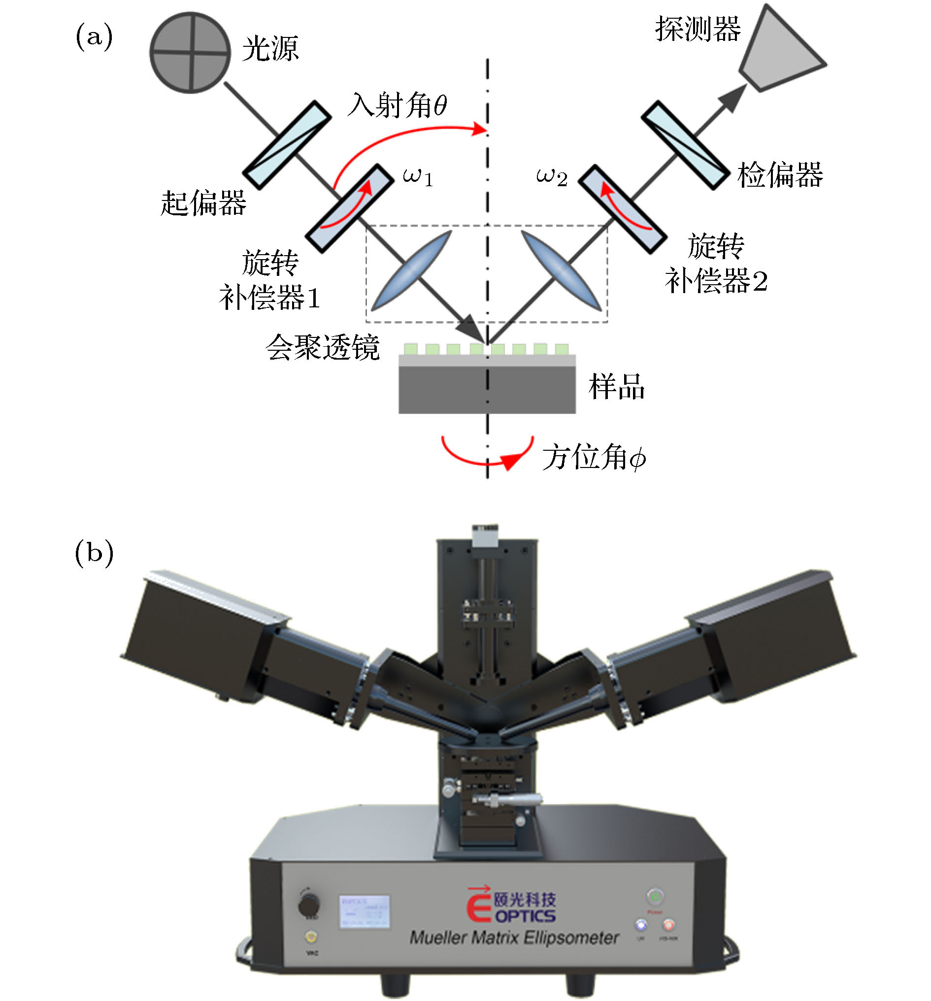 图 2 双旋转补偿器型Mueller矩阵椭偏仪 (a)基本光路; (b)仪器
Figure2. Principle and instrument of the dual rotating-compensator Mueller matrix ellipsometer: (a) Principle; (b) instrument.
实验样品为光栅制作前期工艺中的两个薄膜样品, 样品1是基底为标准硅片(silicon, Si)的单层二氧化硅(silicon dioxide, SiO2)薄膜结构, 其SiO2薄膜厚度的名义值为100 nm, 如图3(a)所示; 样品2为在上述SiO2薄膜结构表面旋涂了一层PMMA的光刻胶培片, 其PMMA薄膜厚度的名义值为385 nm, 如图3(b)所示. 其中, 第1个薄膜样品的待测参数包括SiO2薄膜的厚度值d 1、表面粗糙度c 1及其光学常数折射率n 1和消光系数k 1; 第2个样品的待测参数为PMMA薄膜的厚度值d 2、表面粗糙度c 2及其光学常数折射率n 2和消光系数k 2.
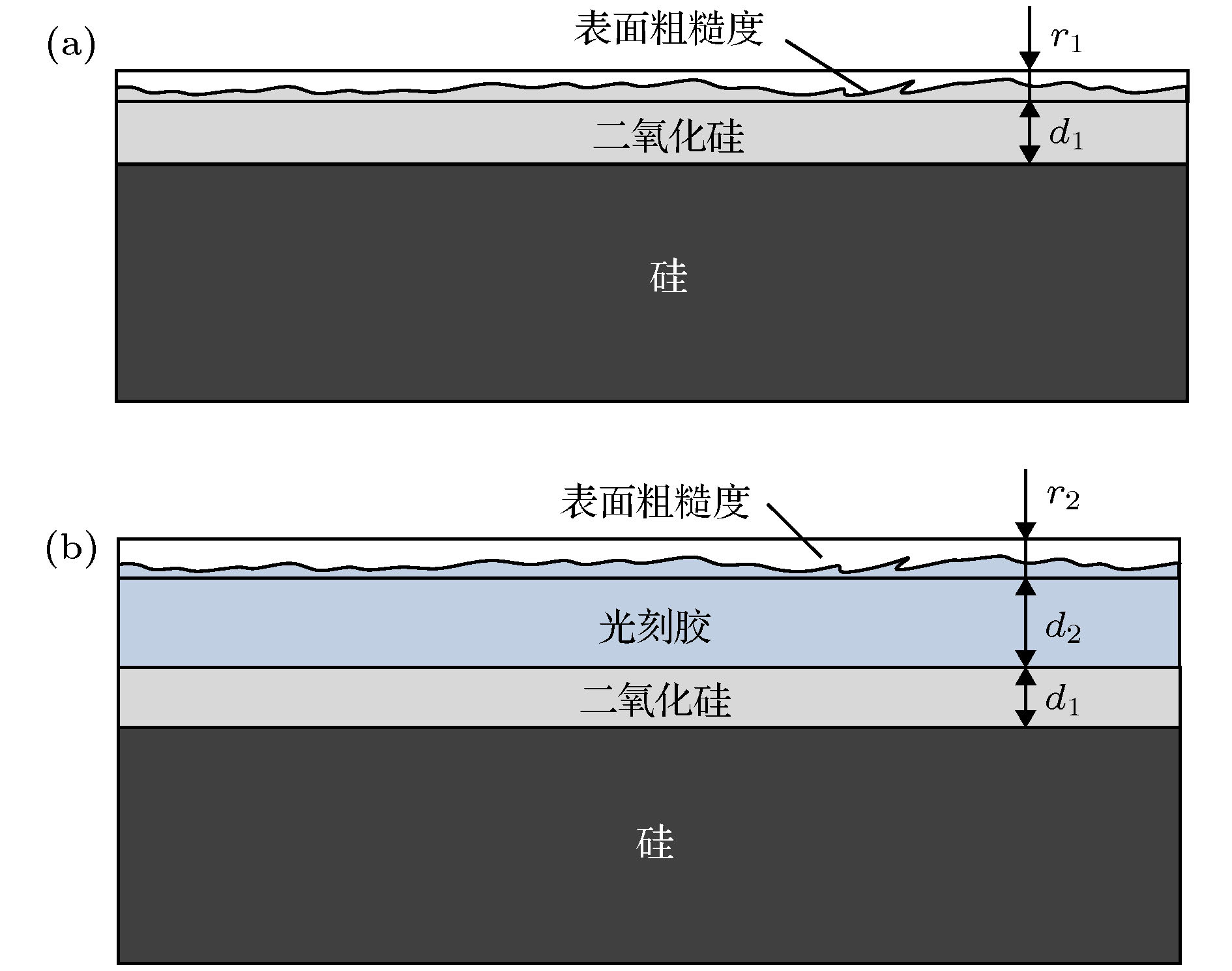 图 3 (a) SiO2薄膜样品; (b) 在SiO2表面旋涂PMMA光刻胶后的薄膜样品
Figure3. (a) The SiO2 sample; (b) the PMMA sample spinning coated on the surface of the SiO2 film.
为了分析椭偏仪入射光对PMMA光刻胶的影响, 首先, 利用ME-L型Mueller矩阵椭偏仪在65°入射角下分别对图3所示的两个薄膜样品进行了20次重复性实验, 各获得20组椭偏参数测量数据, 由于仪器测量时间以及人工操作的时间消耗, 单次测量过程大约耗时15 s, 因此每个样品在入射光下的总暴露时间约为300 s. 然后, 利用上述LM迭代算法分别从每组椭偏参数测量数据中提取出薄膜样品的所有待测参数.
在样品1的参数提取过程中, 对于SiO2光学常数中的n 1和k 1这两个待测参数, 我们采用Cauchy模型[31]对其进行建模, 通过一个三项式来描述材料的折射率n 1, 如(17a)式所示; Urbach尾部的指数吸收则采用(17b)式进行描述.

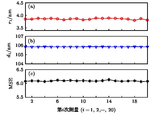 图 4 拟合得到的20组SiO2膜厚d1及其表面粗糙度等效膜厚r1 (a) r1; (b) d1; (c) MSE
Figure4. Extracted results of the thicknesses of SiO2 film h1 and equivalent surface roughness r1: (a) r1; (b) d1; (c) MSE.
 图 5 拟合得到的第1, 5, 10, 15和20组SiO2薄膜光学常数n1和k1的计算值, 以及文献[34]给出的折射率与消光系数 (a) n1; (b) k1
Figure5. Extracted results of the optical constants n1 and k1 of SiO2 film calculated by Cauchy model and the ones from Ref. [34]: (a) n1; (b) k1.
对样品2的待测参数进行逆向提取时, 除了将入射条件(如入射角、入射波长等)、基底硅的光学常数等设为已知量, 还将SiO2薄膜层的厚度、光学常数及粗糙度厚度均固定为样件一中20组提取结果的平均值; 对于PMMA光刻胶光学常数中的n2和k2这两个待测参数, 同样采用Cauchy模型对其进行建模, 其表面的粗糙结构也采用MGEMA模型将其等效为均匀且各项同性的一层薄膜. 在此基础上, 利用LM迭代算法分别对20组椭偏测量数据进行待测参数逆向求取, 待测参数包括d2和r2, 光学常数模型参数

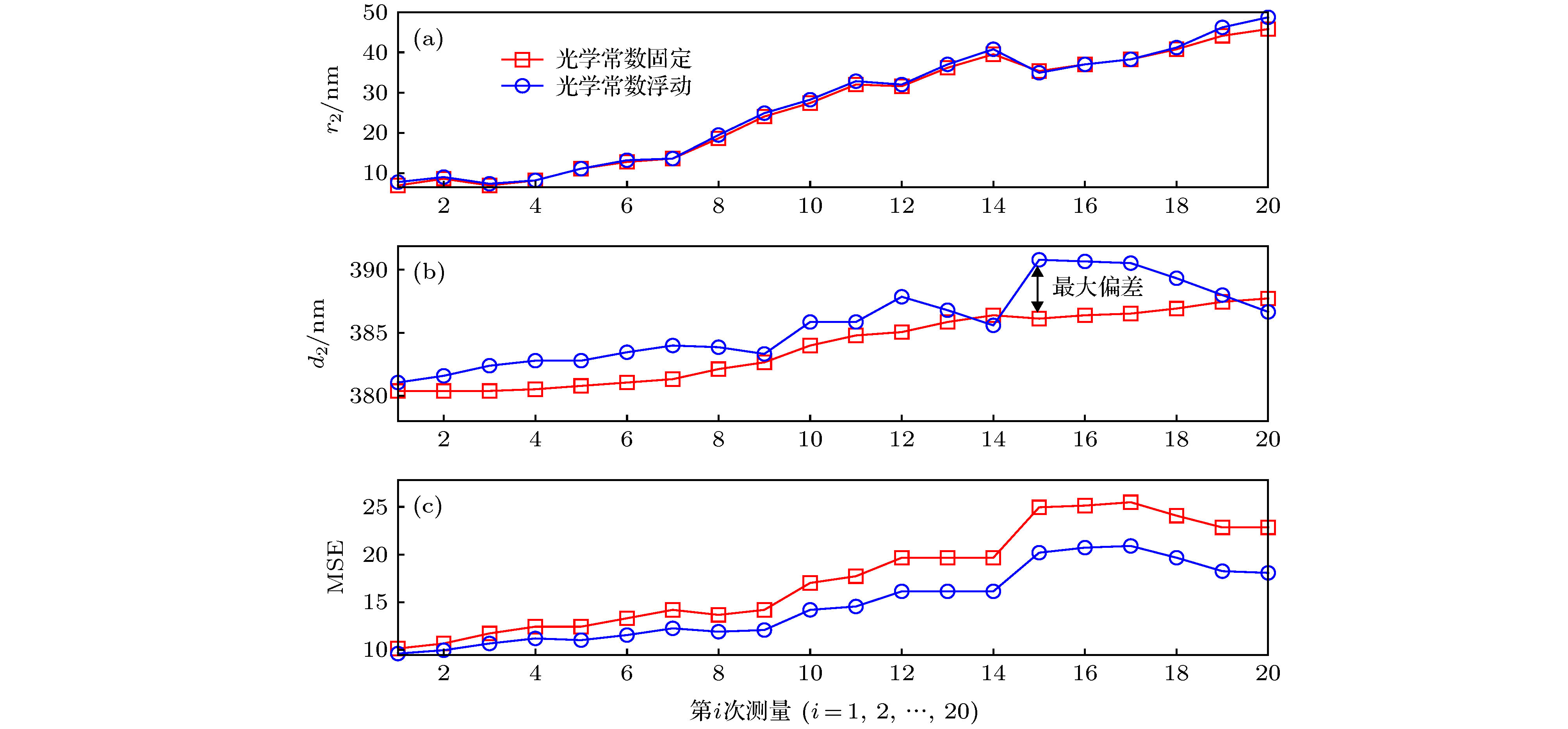 图 6 拟合得到的20组PMMA膜厚d2及其表面粗糙度等效膜厚r2 (a) r2; (b) d2; (c) MSE
Figure6. Extracted results of the thicknesses of PMMA film d2 and equivalent surface roughness r2: (a) r2; (b) d2; (c) MSE.
 图 7 拟合得到的第1, 5, 10, 15和20组PMMA薄膜光学常数n2和k2的计算值 (a) n2; (b) k2
Figure7. Extracted results of the optical constants n2 and k2 of PMMA film calculated by Cauchy model: (a) n2; (b) k2
从图4和图5可以看出, SiO2薄膜样品折射率n1的提取值与文献[34]中的结果几乎保持一致, 且k值的差别为10–5量级(由于k很小, 可忽略不计, 故文献[34]中设定k = 0); SiO2薄膜样品在20次重复性测量数据中拟合得到的折射率n1、消光系数k2以及薄膜厚度d1几乎一致, 其表面粗糙度参数r1的变化幅度也不大, 均位于3.82 nm左右. 由图6和图7可得, 随着入射光照射时间的增加, 重复20次提取得到的PMMA光刻胶折射率n2、消光系数k2、膜厚d2以及表面粗糙度参数r2均存在明显差异, 尤其是第20次得到的k2变化更为剧烈, 可能的原因为PMMA光刻胶到达一定曝光时间后, 其光学特性进入非线性变化区域[35]. 其中, 光刻胶厚度d2大约在380—392 nm的范围内上下波动, 而表面粗糙度r2的变化幅度较大且呈现上升趋势, 其第1次测量的拟合值为7.93 nm, 到第20次测量时为48.43 nm, 变化幅度高达40.5 nm. 对比图6(a)中光刻胶光学常数浮动(蓝色圆圈)与固定(红色方形)的提取结果可得, 光刻胶光学常数的变化对表面粗糙度r2的测量结果影响较小, 而光刻胶厚度d2 (红色方形)明显不同且小于在光学常数浮动时的拟合值(蓝色圆圈), 二者之间的最大差值达到3.5 nm. 此外, 在20次椭偏光谱数据的拟合中, 光学常数固定时得到MSE值均大于其浮动的结果, 即在光刻胶光学常数浮动时, 达到最佳拟合所对应的模型计算椭偏光谱与仪器测量光谱之间的匹配度更高. 上述实验结果表明, SiO2材料不受入射光照射的影响, 而PMMA光刻胶薄膜样品, 尤其是其折射率n2和消光系数k2受到显著影响, 若在待测PMMA薄膜的光学散射测量中将其作为固定量, 则会较大地降低样品薄膜厚度的测量精确度.
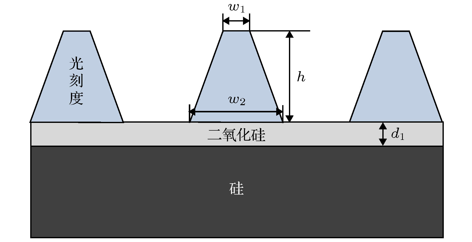 图 8 PMMA光刻胶仿真光栅的结构示意图
Figure8. Geometry of the simulated PMMA grating sample
具体的仿真过程为: 假设光栅结构的真实尺寸为P = 800 nm, w1 = 350 nm, h = 387.42 nm, w2 = 365 nm, PMMA的光学常数n2和k2均取值为图7中的第20次拟合结果, 硅基底和SiO2薄膜的光学常数、厚度等参数信息均与样品2的取值相同; 在入射角θ = 65°、方位角φ = 0°和入射波段为370—870 nm (步长为10 nm)的入射条件下, 利用所建立的基于RCWA的正向光学特性模型计算得到该PMMA光刻胶光栅的一组Mueller矩阵元素, 并将其看作“测量”光谱数据; 在其他参数保持不变的前提下, 将PMMA光学常数n2和k2的取值替换为图6中的第1次拟合结果后, 以顶部线宽w1、线高h和底部线宽w2为浮动的待测参数, 利用LM迭代寻优算法不断调用正向光学特性模型, 并将计算光谱与“测量”光谱进行匹配, 当二者实现最佳匹配后所对应的3个待测形貌参数的拟合值如表1所列, 图9所示为模型计算与“测量”光谱之间的拟合程度.
| 参数名称 | 真实值 | 拟合值 | 绝对误差 |
| 顶部线宽w1/nm | 350.00 | 352.90 | 2.90 |
| 线高h/nm | 387.42 | 387.90 | 0.50 |
| 底部线宽w2/nm | 365.00 | 368.50 | 0.35 |
表1对比PMMA仿真光栅3个待测形貌参数的拟合值与真实值
Table1.Comparison of these three true dimensions and the extracted results of the simulated PMMA grating.
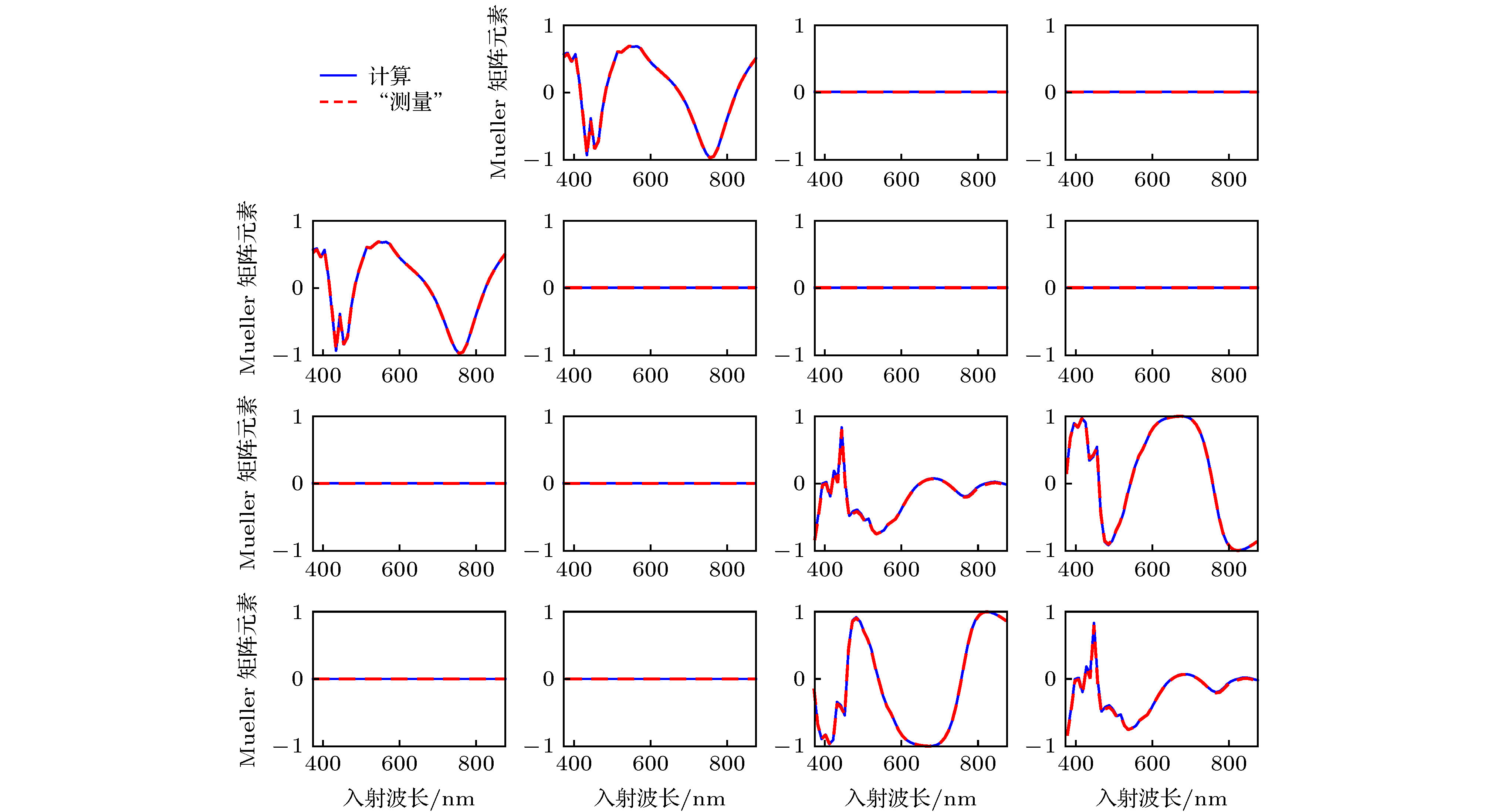 图 9 在入射角θ = 65°、方位角φ = 0°的入射条件下, PMMA光刻胶仿真光栅的模型计算Mueller矩阵光谱与“测量”光谱之间的拟合曲线
Figure9. Fitting results of the calculated and the “ellipsometer-measured” Mueller matrix elements at the incidence and azimuthal angles fixed at θ = 65° and φ = 0°.
由表1可得, 在对“测量”光谱进行待测参数提取时, 改变PMMA光刻胶光学常数n2和k2的取值后, 3个结构参数顶部线宽w1、线高h和底部线宽w2的提取结果在一定程度上偏离于真实值. 其中, 引起待测形貌参数顶部线宽w1的测量误差为最大, 达到了2.90 nm. 本文第3节中光刻胶薄膜的测量实验研究证明了光刻胶的光学常数受到椭偏仪入射光的照射影响后会发生明显的变化, 这里光刻胶光栅的仿真结果表明了光刻胶光学常数的变化将较大地降低光栅结构几何形貌参数的测量准确度. 因此, 针对半导体制造工业中光刻胶纳米结构的光学散射测量而言, 其光学常数会随着入射光照射时间增加而发生变化这个特性将不能再被忽略, 这对于实现光刻胶纳米结构三维形貌参数的高精确度测量具有较为重大的指导意义.
