全文HTML
--> --> -->自2004年Geim研究组成功获得石墨烯以来, 石墨烯及其相关器件的研究受到了广泛关注[31-34], 扶手椅型和锯齿型石墨烯纳米带[35,36]作为基本结构经常被用于石墨烯基分子电子器件设计. 氧化石墨烯/二氧化硅复合材料[37]被证明在323—473 K的温度范围内具有优异的介电常数和电磁干扰屏蔽性能. Cao等[38]系统地研究了二维材料的电子输运、偶极弛豫和磁共振等电磁响应起源, 他们还探讨了碳基材料和过渡金属化合物的电子结构、电磁响应和能量转换以及它们之间的关系[39]. Zhang等[40]系统地研究了图案化二维材料先进制造技术及其电子结构和物理特性. Fang等[41]基于玻尔兹曼输运方程和二维电子气理论建立了多层石墨烯电导率的计算模型. Cao等[42]提出“物质基因测序”方法, 从实验和理论上探讨热驱动的弛豫和电荷输运性质, 他们还发现超薄轻质石墨烯复合材料在高温下具有高效的微波吸收性能以及热稳定性介电常数[43]. Wen等[44]的研究表明, 多壁碳纳米管/二氧化硅复合材料在100—500 ℃的温度范围内对8.2—12.4 GHz范围内的微波辐射具有电磁干扰屏蔽性能. 此外, 喹啉是冶金、染料以及聚合物的重要中间体, 是结构比较简单的有机共轭小分子, 具有来源广泛、结构可设计、易于合成和便于化学结构修饰等特点, 是分子电子器件领域的研究热点之一, 从物理的角度探讨嵌于石墨烯纳米带电极间的同分异构喹啉分子电子器件的输运性质, 可为设计制作性能优良的分子电子器件提供理论依据.
本文基于密度泛函理论(DFT)与非平衡格林函数的(NEGF)相结合的第一性原理计算方法, 系统地研究了通过碳原子连接的同分异构喹啉分子嵌于石墨烯纳米带电极间的分子电子器件输运性质. 研究结果表明, 器件电流在偏压[–0.3 V, +0.3 V]范围内呈线性变化, 电流在[–0.4 V, –0.9 V]和[+0.5 V, +0.8 V]范围内随着偏压的增大而减小, 呈现显著的负微分电阻效应. 此外, 当喹啉分子平面与石墨烯纳米带电极间存在一定夹角时, 器件电流呈现明显的负微分电阻效应且与喹啉分子平面旋转方向无关; 当喹啉分子平面与石墨烯纳米带电极垂直时, 器件电流截止. 以上研究结果得到偏压窗内透射系数积分以及零偏压下实空间电荷密度分布的有力印证, 可为设计制作基于同分异构喹啉分子的分子开关和负微分电阻器件提供理论依据.
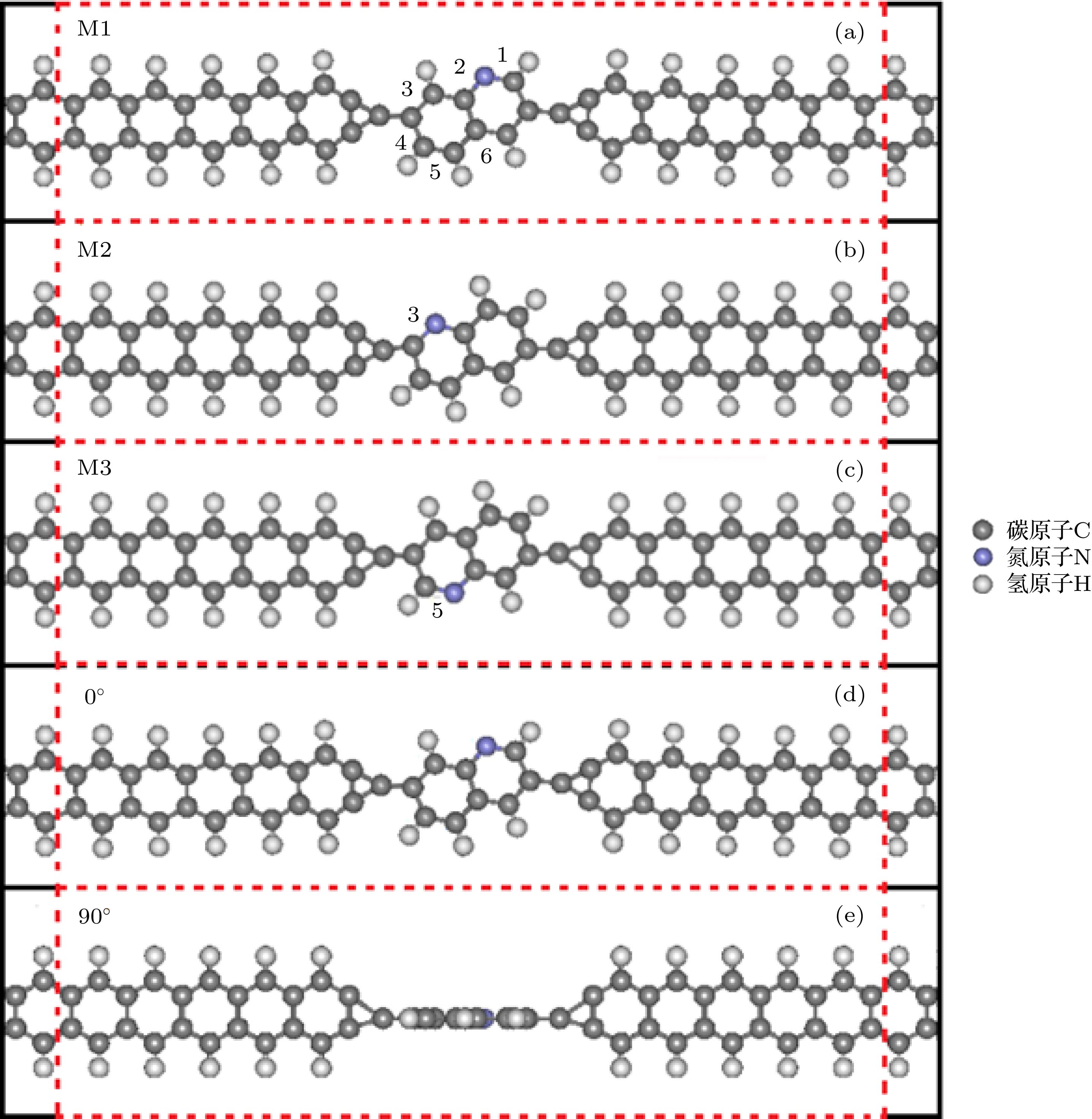 图 1 由半无限长锯齿型石墨烯纳米带左电极/中心散射区/半无限长锯齿型石墨烯纳米带右电极组成的ZGNR/C9H5N/ZGNR分子电子器件结构示意图, 红色方框区域表示中心散射区 (a)—(c)分别对应喹啉C9H5N分子中氮原子N处于编号2, 3和5处; (d)和(e)给出喹啉C9H5N分子平面与石墨烯纳米带电极平面成0°和90°时的模型
Figure1. ZGNR/C9H5N/ZGNR molecular electronic device schematic diagram consisted of a semi-infinite ZGNR left electrode/a central scattering region/a semi-infinite right ZGNR electrode, the red dashed line area represents the central scattering region. (a)?(c) denotes the marked 2nd, 3rd and 5th N atom of the C9H5N molecular; (d) and (e) illustrates the model of the 0° and 90° angle between the C9H5N molecule and graphene nanoribbon electrodes, respectively.
我们的计算采用DFT与NEGF相结合的第一性原理计算方法[45-48], 研究过程中选择自洽循环哈密顿量, 局部密度近似[49]LDA_PZ交换相关势, 费米温度为100 K, 能量截断半径取为80 Hartree, 对所有原子选用双极化DZP基函数组. x和y方向为真空方向, z方向为输运方向. 对应x, y和z方向, 左电极、中心散射区和右电极的K点取样分别为1 × 1 × 100, 1 × 1 × 1和1 × 1 × 100. 此外, 我们采用较大的基函数组、较高的能量截断半径以及广义梯度近似[50,51]下Perdew-Burke-Ernzerhof泛函[52-55]验证了研究结果的准确性.
基于格林函数方法计算得到的透射系数为

推迟格林函数

L/R代表左/右电极, E表示从做左电极L所有通道并散射到右电极R的能量, VB是左、右电极间的偏置电压,


 图 2 器件电流-电压(I-V)曲线(a)和电导(b)
Figure2. The current-voltage (I-V) curve (a) and conductance (b) of the device.
为进一步分析图2中电流-电压曲线和电导变化规律, 图3给出0, ± 0.4 V, ± 0.9 V以及 ± 1.5 V 偏压下器件M1, M2和M3的透射谱, 费米能级取为能量参考点, 偏压窗为[–VB/2, +VB/2]即图中的黑色虚线之间的区域. Landauer-Büttiker公式表明, 分子器件的电流可以通过对偏压窗内的透射系数积分得到[56]. 从图3(a)—图3(c)可以看出, 零偏压下费米能级处存在透射峰, 器件是金属性的, 电流在0—±0.3 V低偏压范围内呈线性变化(如图2(a)所示); 零偏压下费米能级处的透射峰随着偏压的增加逐渐降低. 随着偏压的增加, 低于费米能级的第一隧穿峰逐渐增大并向费米能级方向移动, 导致随着偏压窗的增大, 积分面积呈现先增大后减小再增大的变化, 有力印证了图2中电流和电导随偏压的变化.
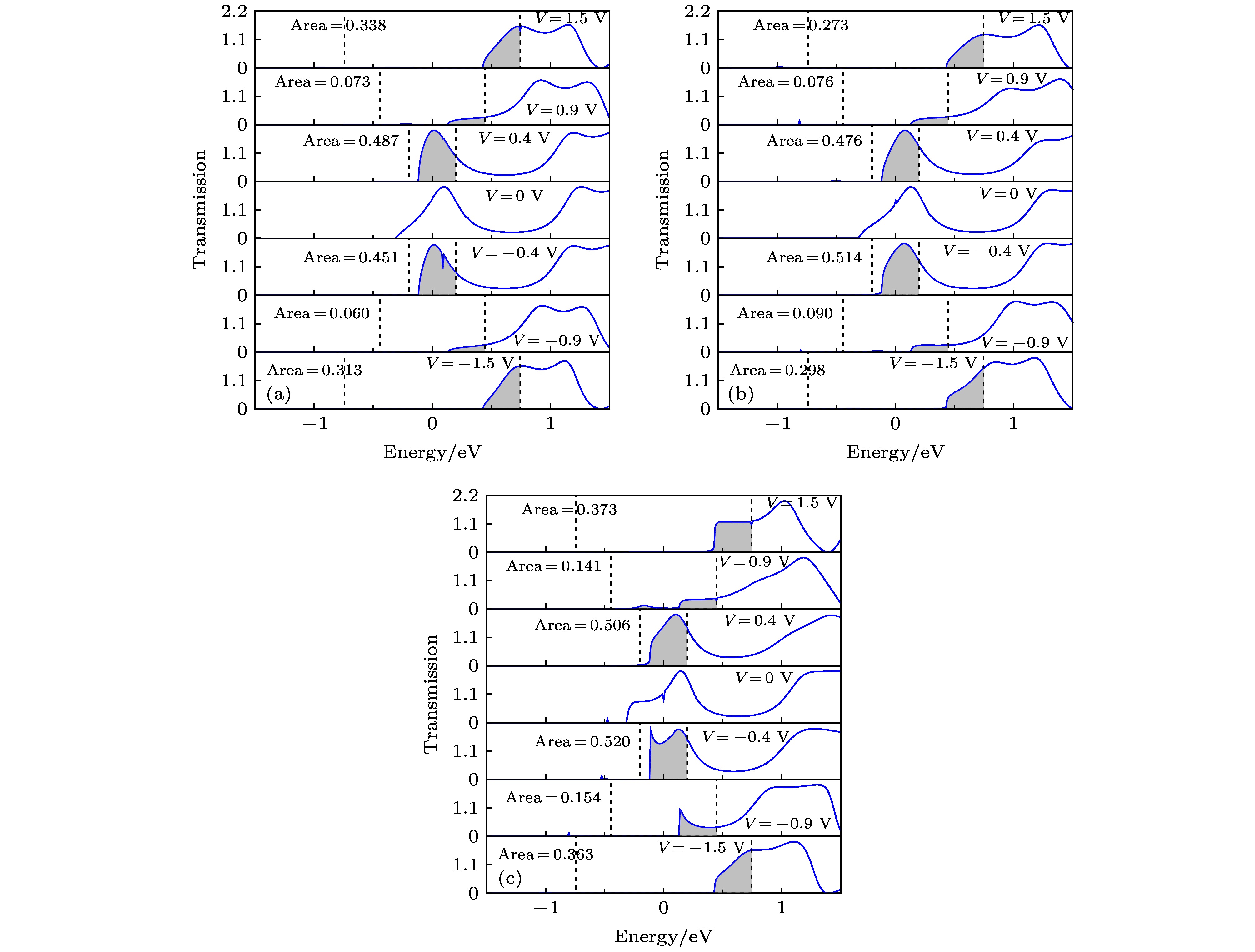 图 3 器件(a) M1、(b) M2和(c) M3在0, ±0.4 V, ±0.9 V以及±1.5 V偏压下的透射谱, 图中的黑色虚线和阴影部分面积分别表示偏压窗和偏压窗内的透射系数积分面积
Figure3. The transmission spectrum of the device (a) M1, (b) M2 and (c) M3 under the bias voltage of 0, ±0.4 V, ±0.9 V and ±1.5 V, where the (black) dashed lines and shaded area denote the bias window and the integrated area of the transmission coefficient in the bias window, respectively.
将喹啉C9H5N分子平面往垂直纸面向里旋转方向定义为正, 图1(d)和1(e)给出喹啉C9H5N分子平面与石墨烯纳米带电极成0°和90°时的模型. 图4中给出M1器件喹啉C9H5N分子平面与石墨烯纳米带电极成0°, 30°, 45°, 60°, 90°和–90°时的I-V曲线和电导. 在0—± 0.3 V偏压范围里, 如图4(a)中的方块标记的黑色实线、圆点标记的红色长虚线和上三角标记的蓝色短虚线所示, 喹啉C9H5N分子平面与石墨烯纳米带电极成0°, 30°和45°时的I-V曲线呈线性变化, 但电流在偏压绝对值超过0.3 V后随着角度的增大迅速减小; 当喹啉C9H5N分子平面与石墨烯纳米带电极成60°时, 如图4(a)中下三角标记的绿色点线所示, 电流在 ± 0.3 V偏压时大幅减小, 在 ± 0.8 V—± 1.2 V范围内趋近于0; 当喹啉C9H5N分子平面与石墨烯纳米带电极成 ± 90°时, 如图4(a)中的菱形标记的紫色点虚线和左三角标记的黄色点线所示, 电流几乎为0, 即电流截止, 且喹啉C9H5N分子平面与石墨烯纳米带电极成–90°时呈现与90°时同样的变化, 说明电流变化与喹啉分子平面旋转方向无关, 只与旋转的角度有关. 此外, 图4(b)中电导在偏压绝对值超过0.3 V后, 随着喹啉分子平面与石墨烯纳米带电极间夹角的增大迅速减小, 有力地印证了电流的变化规律.
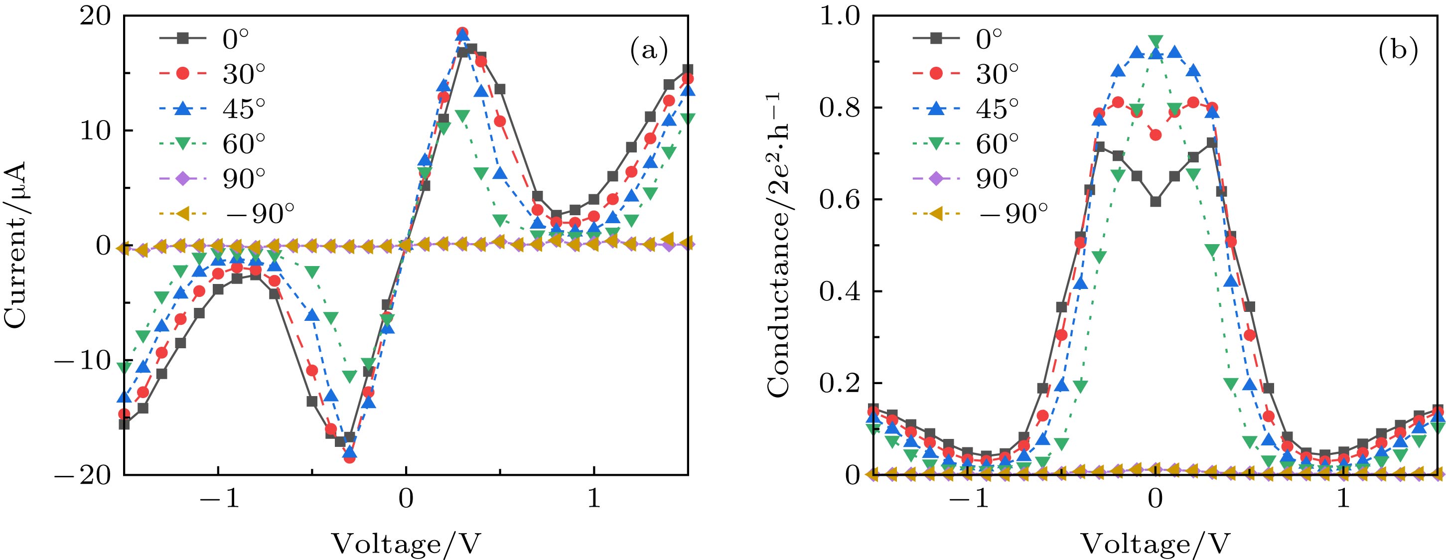 图 4 M1器件喹啉C9H5N分子平面与石墨烯纳米带电极成0°, 30°, 45°, 60°, 90°和–90°的(a)I-V曲线和(b)电导
Figure4. The (a) I-V curve and (b) conductance of the M1 device when the angle between the C9H5N molecule and graphene nanoribbon electrodes is 0°, 30°, 45°, 60°, 90° and –90°, respectively.
为进一步解释图4中电流和电导变化规律, 图5给出0, ± 0.3 V, ± 0.9 V以及 ± 1.5 V偏压下喹啉C9H5N分子平面与石墨烯纳米带电极成0°, 30°, 45°, 60°和90°的透射谱, 其中的黑色虚线和阴影部分面积分别表示偏压窗和偏压窗内透射系数的积分面积. 从图5(a)—(d)可以看出, 在0偏压下费米能级处存在透射峰, 器件是金属性的, 电流在低偏压范围内呈线性变化(如图4(a)所示), 费米能级处的透射峰随着偏压的增加逐渐降低, 直至最后消失. 随着偏压的增加, 低于费米能级的第一和第二隧穿峰逐渐增强并向费米能级移动, 导致随着偏压窗的增大, 积分面积先增大后减小再增大, 从而解释了图4中电流和电导变化的原因以及负微分电阻现象. 当喹啉C9H5N分子平面与石墨烯纳米带电极成60°角时, 积分面积在偏压为± 0.3 V附近大幅度减小, 当偏压增大到 ± 1.0 V时积分面积接近于0; 当喹啉C9H5N分子与石墨烯纳米带电极成90°时, 积分面积在所有偏压下趋于零, 即没有电流通过. 我们进一步研究了电极宽度对结果的影响, 发现电极宽度变大时, 所观测到的负微分电阻效应及开关效应仍然存在.
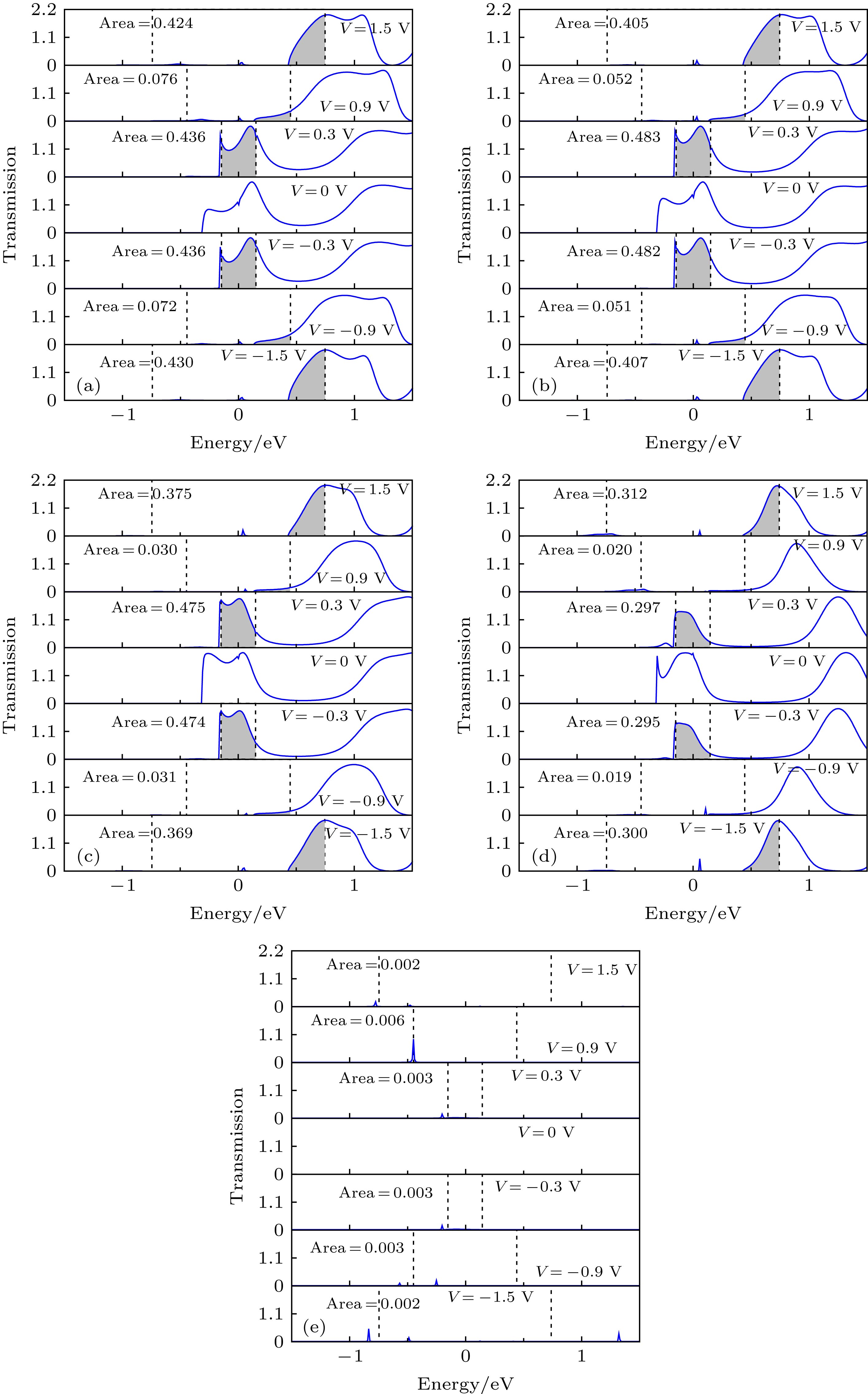 图 5 偏压0, ± 0.3 V, ± 0.9 V以及 ± 1.5 V下喹啉C9H5N分子平面与石墨烯纳米带电极分别成 (a) 0°, (b) 30°, (c) 45°, (d) 60°和(e) 90°时的透射谱, 图中的黑色虚线和阴影部分面积分别表示偏压窗和偏压窗内透射系数积分面积
Figure5. The transmission spectra for the angle between the C9H5N molecules and graphene nanoribbon electrodes is (a) 0°, (b) 30°, (c) 45°, (d) 60° and (e) 90°, respectively, under the bias voltage of 0, ± 0.3 V, ± 0.9 V and ± 1.5 V, where the (black) dashed lines and shaded area denote the bias window and the integrated area of the transmission coefficient in the bias window, respectively.
图6中给出零偏压下喹啉C9H5N分子平面与石墨烯纳米带电极成0°, 30°, 45°, 60°, 90°和–90°时的透射谱. 从图中可以看出, 喹啉C9H5N分子平面与石墨烯纳米带电极成0°, 30°, 45°和60°角度时, 费米能级处均呈现尖锐的透射峰; 当喹啉C9H5N分子平面与石墨烯纳米带电极成90°和–90°时, 透射谱在非常宽的带隙范围内为0, 很好地印证了图4中的电流-电压曲线以及电导变化规律.
 图 6 零偏压下, 喹啉C9H5N分子平面与石墨烯纳米带电极成0°, 30°, 45°, 60°, 90°和–90°角度下的透射谱, 其中红色虚线表示费米能级
Figure6. The transmission spectrum of the C9H5N molecule and the ZGNR electrodes at the angle of 0°, 30°, 45°, 60°, 90° and –90° under the 0 bias, where the (red) dashed line denotes the Fermi level.
图7给出零偏压下喹啉C9H5N分子平面与石墨烯纳米带电极成0°, 60°, 90°, –90°时的实空间电荷密度, 直观地展现电荷的分布情况. 从图7(a)和图7(b)可以看出, 当喹啉C9H5N分子平面与石墨烯纳米带电极成60°时, 中心区喹啉C9H5N分子电荷分布较多, 但是分子与电极连接处存在电荷缺口, 这就解释了喹啉C9H5N分子平面与石墨烯纳米带电极成60°时, 电导在0偏压下较大但随着偏压的增加急剧减小的原因. 比较图7(c)和图7(d)可以发现, 当喹啉C9H5N分子平面与石墨烯纳米带电极成90°或–90°时, 中心区喹啉C9H5N分子电荷分布较多, 电极上电荷分布较少, 不利于电荷输运, 从另一方面解释了喹啉C9H5N分子平面与石墨烯纳米带电极成90°或–90°, 电流几乎为0.
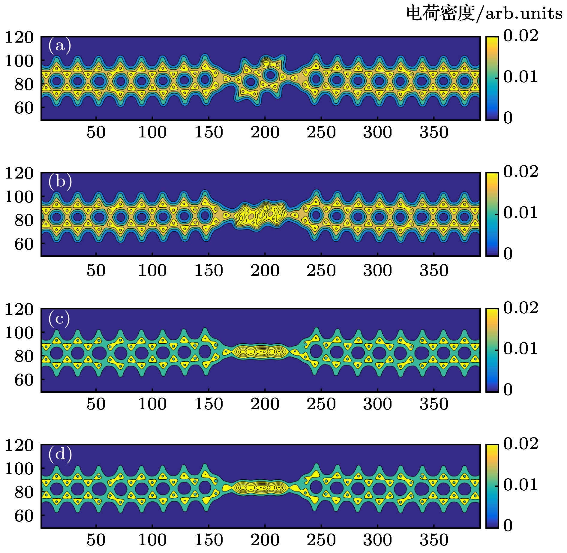 图 7 零偏压下, 喹啉C9H5N分子平面与石墨烯纳米带电极成 (a) 0°, (b) 60°, (c) 90°和(d) –90°时的实空间电荷密度
Figure7. The real space charge density for the angle between the C9H5N molecule and graphene nanoribbon electrodes is (a) 0°, (b) 60°, (c) 90° and (d) –90°, respectively under the 0 bias voltage.
