Abstract:Very recently, higher-order topological insulators and superconductors have attracted wide attention and aroused the great interest of researchers. Owing to their unconventional bulk-boundary correspondence, higher-order topological insulators and superconductors possess novel boundary modes whose dimensions are always lower than the first-order (or say conventional) topological insulators and superconductors, provided that their bulk dimensions are the same. The essence of higher-order topological phase is the formation of Dirac-mass domain walls on the gapped one-dimensional lower boundary. Roughly speaking, the origins of the formation can be classified as " intrinsic” and " extrinsic” type. For the former case, the formation of domain walls is forced by symmetry, suggesting that the resulting higher-order topological phases can be taken as topological crystalline phases. For this case, the domain walls are quite robust if the corresponding symmetry is preserved. For the latter case, the domain walls are formed simply because the one-dimensional lower boundary modes are gapped in a nontrivial way, however, the nontrivial way is not forced by symmetry. For this case, the domain walls are also stable against perturbations as long as the separations between them are large enough. The domain walls can have various patterns, which indicates that the higher-order topological phases are very rich. In this paper, we first reveal the connection between the higher-order topological phase and the first-order topological phase. Concretely, we show how to realize a higher-order topological phase by breaking some symmetries of a first-order topological phase, as well as stacking lower-dimensional first-order topological systems in an appropriate way. After these, we review the recent progress of theoretical and experimental study of higher-order topological insulators and superconductors. For the higher-order topological insulators, we find that the electronic materials are still laking though a lot of experimental realizations have been achieved. For higher-order topological superconductors, we find that their experimental realization and investigation are still in the very primary stage though quite a lot of relevant theoretical studies have been carried out. In order to comprehensively understand this newly-emerging field there are still many things to be done. Keywords:higher-order topological insulator/ higher-order topological superconductor/ bulk-boundary correspondence
全文HTML
--> --> --> 1.引 言寻找和理解新奇的物态并对它们进行分类是凝聚态物理发展的核心方向之一. 在二十世纪, 对物态的认识和理解的一大重要成就是朗道的相与相变理论. 根据此理论, 不同的物相由不同的局域序参数刻画, 而不同的序参数对应着不同的对称性破缺. 此理论的广泛适用性在很长一段时间内让物理学家以为所有的物态均可以由局域的序参数刻画, 而不同物态间的相变对应着不同的对称性破缺. 然而, 随着二维Kosterlitz-Thoulss相变理论[1]的提出和强磁场下二维电子气中的整数和分数量子霍尔效应的发现[2,3], 大家逐渐认识到存在新的物态, 且对这些物态的描述超越了朗道的相与相变理论[4]. 此类新的物态即所谓的拓扑物态. 与对称破缺有序相不同(如铁磁相), 拓扑物态无法由局域的序参数完美刻画, 而需要利用数学中的拓扑不变量的概念. 拓扑不变量刻画的是封闭流形的全局性质, 它最重要的特征是它只能取离散的数值而不能连续变化. 这意味着只要流形的几何没有发生突变, 如空洞的数目, 那么即使流形的几何性质在局域上发生了变化, 拓扑不变量也不会发生改变. 反映在物理上, 这对应拓扑物态存在非常稳定的物理性质. 在这方面最具代表性的例子是二维整数量子霍尔效应[2,5]. 根据半经典理论, 二维电子气的霍尔电阻应随着磁场线性增加, 然而在实验上却观察到一系列的平台[2]. 在低温下这些平台是如此地不依赖于样品的细节, 以至于现在它们被作为电阻的标准单位[6]. 拓扑物态的发现激发了广泛的关注和研究. 这一方面是由于发现拓扑物态具有非常丰富的物理, 如分数化现象, 分数统计等[7]; 另一方面则是由于拓扑物态呈现出诱人的应用前景. 在对拓扑物态的研究中, 人们发现拓扑物态存在一个普遍的特征, 即所谓的“体-边对应”. 它指如果刻画“体”的拓扑不变量非平凡, 那么在边界上将存在无能隙模式. 由于受拓扑保护, 这些无能隙模式具有无耗散或者低耗散的特征, 因而一个直接的应用就是电子器件. 整数量子霍尔效应呈现的霍尔平台即是由于边界上存在无能隙的手征模式. 这些手征模式由于无法被向后散射, 因而它们的传输没有耗散, 是理想的导电通道. 继整数和分数量子霍尔效应发现之后, 拓扑物态研究的一个重要突破来自于二维量子自旋霍尔效应(又称为二维拓扑绝缘体)的理论预言[8-11]和实验证实[12]. 二维量子自旋霍尔效应是全新的拓扑物态. 由于具有时间反演对称性, 它对应的无能隙边界态总是成对出现, 且每一对的两支模式总是沿着相反方向传输[8-11], 非常不同于整数量子霍尔效应的手征边界态. 二维量子自旋霍尔效应开启了拓扑能带理论的研究. 根据能带理论, 二维的量子自旋霍尔效应很快被推广到三维, 产生了三维拓扑绝缘体的概念[13-15]. 理论研究发现在只要求时间反演对称性的条件下, 二维和三维拓扑绝缘体能带的拓扑性质均可以用Z2不变量刻画[9,13-15], 这也和整数量子霍尔效应的整数分类完全不同. 另外, 在对二维拓扑绝缘体的研究中, 已认识到能带反转和自旋轨道耦合对实现拓扑绝缘体的重要性[11]. 能带反转提供了一个判断真实材料是否为拓扑绝缘体的简单判据. 在拓扑材料的预言和实验探测上, 这一简单的判据起到了非常重要的指导作用. 由于在哈密顿量的描述形式上, 绝缘体和超导体并无差异, 因此在拓扑绝缘体的概念出现之后, 拓扑超导体的概念也随之被提出. 相似地, 当超导体具有非平凡的拓扑性质时, 它的边界上也将存在无能隙模式. 不过, 一个重要的区别是拓扑绝缘体的边界态是带电的, 而拓扑超导体的边界态是电中性的. 这一区别具有重要的物理后果. 在对一维的p-波超导体的研究中, Kitaev[16]发现当超导体处于拓扑相时, 其每一端均存在一个稳定的Majorana零模, 即反粒子是自身的模式. 由于两个Majorana零模等价于一个狄拉克费米子, 而一个狄拉克费米子的占据和非占据两种状态可以构建一个量子比特, 这意味着一个量子比特的信息可以存储在两个分隔很远的Majorana零模上. 这种非局域的信息存储方式可以保证信息能够对抗环境的噪声. 另外, 研究发现Majorana零模具有非阿贝尔的统计[17]. 当存在多个Majorana零模时, 对它们进行编织操作等效于对量子比特做逻辑门操作, 因而可用于拓扑量子计算[18-20]. 正是由于在拓扑量子计算方面的潜在应用, 近年来实现拓扑超导体和探测其中的Majorana零模一直是凝聚态领域最活跃的研究方向之一[21-24]. 由于哈密顿量形式上的相似, 拓扑绝缘体和拓扑超导体可以放在同一框架下进行分类. 早期的拓扑分类是根据哈密顿量是否具有时间反演对称性、粒子-空穴对称性和手征对称性(或子格对称性)[25, 26]. 根据这三个对称性, 一共存在十个对称类[25, 26]. 在任意维度, 十个对称类中有五个对称类允许存在非平凡的拓扑相. 后来晶体对称性的重要性被认识到, 相应地产生了拓扑晶体绝缘体和拓扑晶体超导体的概念[27]. 由于晶体对称性的丰富, 拓扑物态的种类相应地也变得非常丰富. 在最新的研究中, 人们发现已知的几万种材料中有超过百分之二十是拓扑非平凡的材料[28-30], 展现出拓扑物态的普遍. 近年来对拓扑物态的研究进一步产生了高阶拓扑绝缘体和高阶拓扑超导体的概念[31-35]. 高阶拓扑物态的“高阶”体现在其体-边对应关系上. 对d维的传统拓扑绝缘体和拓扑超导体, 我们知道其具有(d-1)维的无能隙边界态[21,36]. 如三维的拓扑绝缘体具有二维的狄拉克表面态, 二维的拓扑绝缘体具有一维的螺旋边界态. 而对一个d维的n阶拓扑物态, 其具有(d-n)维的无能隙边界态, 其中$ 1 \leqslant n \leqslant d $, 如图1所示. 例如, 二维二阶拓扑绝缘体具有零维的边界态, 而三维二阶拓扑绝缘体具有一维的无能隙边界态. 根据这个定义, 传统的拓扑绝缘体和拓扑超导体也被称为一阶拓扑绝缘体和一阶拓扑超导体. 图 1 拓扑物态的边界态示意图 $n = 1$的行对应传统的拓扑物态, 其具有比系统维度低一维的无能隙边界态; $n \geqslant 2$的行对应高阶拓扑物态, 其具有比维度低n维的无能隙边界态 Figure1. A schematic diagram of the boundary modes of topological matter. The line with $n = 1$ corresponds to conventional topological matters which host gapless modes whose dimensions are one-dimensional lower than the system dimension. The lines with $n \geqslant 2$ correspond to higher-order topological matters which host gapless modes whose dimensions are n-dimensional lower than the system dimension.
其中, ${{{\sigma}}_{x, y, z}}$和${{{s}}_{x, y, z}}$为泡利矩阵, 分别作用在子能带(subbands)自由度和自旋自由度上; 为了简化表达式, 晶格长度在本文中将自始至终设置为1; A, B和M为常数. 不失一般性, 我们考虑A和B均为正数. 刻画此哈密顿量的${Z_2}$不变量[37]具有下面的形式:
其中$A(\ell ) = A$, 而$m(\ell )$在I, II, III, IV四个边界上的取值分别为$ - \varLambda M/2 B$, $\varLambda M/2 B$, $ - \varLambda M/2 B$, $\varLambda M/2 B$. 由此可以看出, 在角的地方$A(\ell )$保持不变, 而$m(\ell )$的符号将发生改变. 这意味着在角的地方正好形成了一个狄拉克质量的畴壁. 根据Jackiw-Rebbi理论[39], 这样的畴壁将束缚一个零维的零能量束缚态. 由于四个角都形成了畴壁, 因此一共存在四个零能量束缚态. 由于这些零能量束缚态存在于系统的角上, 因此它们也被称为角模(corner modes). 利用边界态理论, 可以清晰地看出如何从一阶拓扑物态转变为高阶拓扑物态. 简言之, 如果从一个d维的一阶拓扑物态出发, 要实现一个d维的高阶拓扑物态, 首先需要破坏保护一阶拓扑物态无能隙边界态的对称性, 如保护一阶拓扑绝缘体的时间反演对称性; 其次, 破坏对称性的方式需要具有各向异性的特点. 虽然利用边界态理论时为了分析上的简单, 我们假设了新引入的项可以当作微扰, 但这并不意味着上面的图像和结论只有当Λ很小时成立. 为了显示这一事实, 直接根据(9)式中的格点哈密顿量数值计算Λ项对边界态的影响. 计算结果确定了即使Λ项不能当作微扰, 上述的图像依然成立, 如图2所示. 图 2 从一阶拓扑绝缘体到二阶拓扑绝缘体 (a) 沿x方向取开放边界条件(${L_x} = 100$), 沿y方向取周期边界条件, 参数为$M = B = A = 1$, $\varLambda = 0$, 对应BHZ模型, 能谱反映出无能隙边界态的存在; (b) 插图中红点对应的能量本征态的波函数分布, 参数同(a), 但沿x和y两个方向均取开放边界条件; 红色的深浅对应波函数分布概率的大小, 可以看出对一阶拓扑绝缘体, 波函数分布在整个边界上; (c) 边界条件和参数同(a), 除了此处$\varLambda = 0.5$, 可看出Λ项的出现让边界态打开了能隙; (d) 零模的波函数分布, 参数同(c), 但沿x和y两个方向均取开放边界条件; 从插图中可发现存在四个零模, 这四个零模的波函数局域在四个角上 Figure2. From first-order topological insulator to second-order topological insulator. (a) Energy spectra for a sample with open boundary condition in the x direction (the system size ${L_x} = 100$) and periodic boundary condition in the y direction. Parameters are $M = B = A = 1$, $\varLambda = 0$, which corresponds to the original BHZ model. The energy spectra reflect the existence of gapless boundary modes. (b) the density profile of a boundary mode. The parameters are the same as in (a), but now open boundary conditions are taken both in the x and y directions. One can see that the density profile of the boundary mode distributes over the whole boundary. (c) the boundary conditions and parameters are the same as in (a), except now $\varLambda = 0.5$. One can see that the presence of the Λ term opens a gap for the boundary modes. (d) the density profiles of zero modes.The parameters are the same as in (c), but now open boundary conditions are taken both in the x and y directions. One can see that there are four zero-energy modes in the inset. Their wave functions are found to be localized around the corners.
其中${t_x}$和${t'_x}$为最近邻格点间的跃迁系数, 如图3(a)所示. ${{{\sigma}} _i}$为泡利矩阵, 作用在$ ({\rm{A}}, {\rm{B}})$子格上. 此模型由于具有子格(或手征)对称性(算符为${{{\sigma}} _z}$), 其拓扑性质由绕数(winding number)刻画, 图 3 从一维一阶拓扑绝缘体到二维二阶拓扑绝缘体 (a) 一维SSH链的示意图; (b) 利用一维SSH链构造二维二阶拓扑绝缘体, 每个单位元胞中有一个${\text{π}}$磁通 Figure3. Constructing two-dimensional second-order topological insulator by using one-dimensional topological insulator: (a) A schematic diagram of the SSH chain; (b) using the one-dimensional SSH chains to construct a two-dimensional second-order topological insulator, within each small square, there is a ${\text{π}}$-flux.

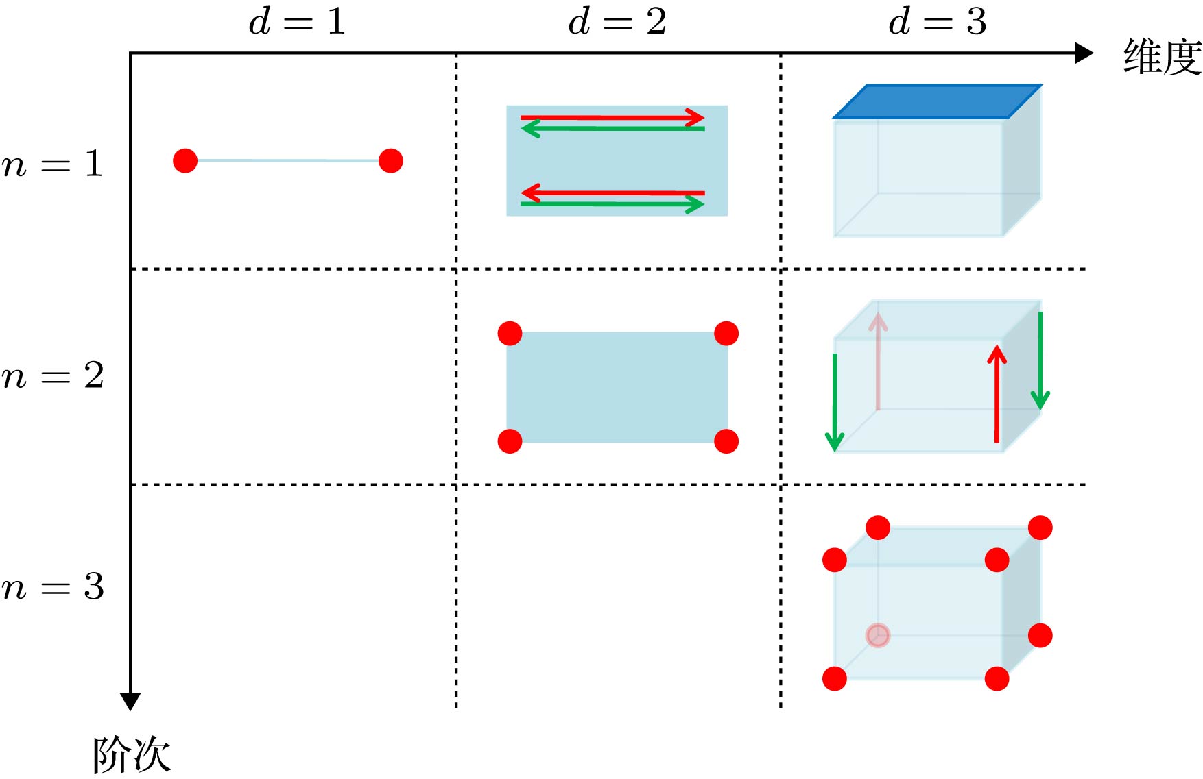 图 1 拓扑物态的边界态示意图


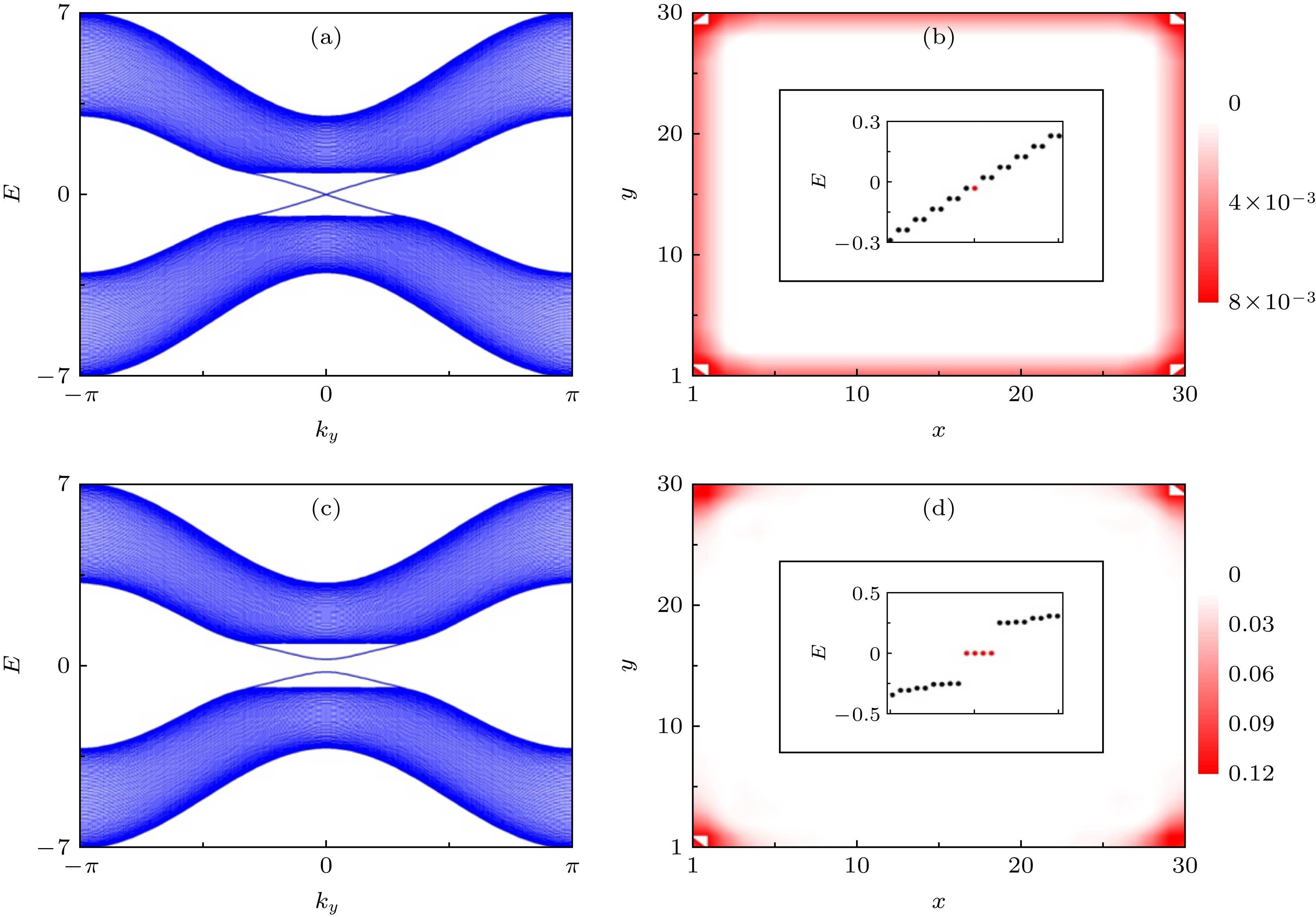 图 2 从一阶拓扑绝缘体到二阶拓扑绝缘体 (a) 沿x方向取开放边界条件(


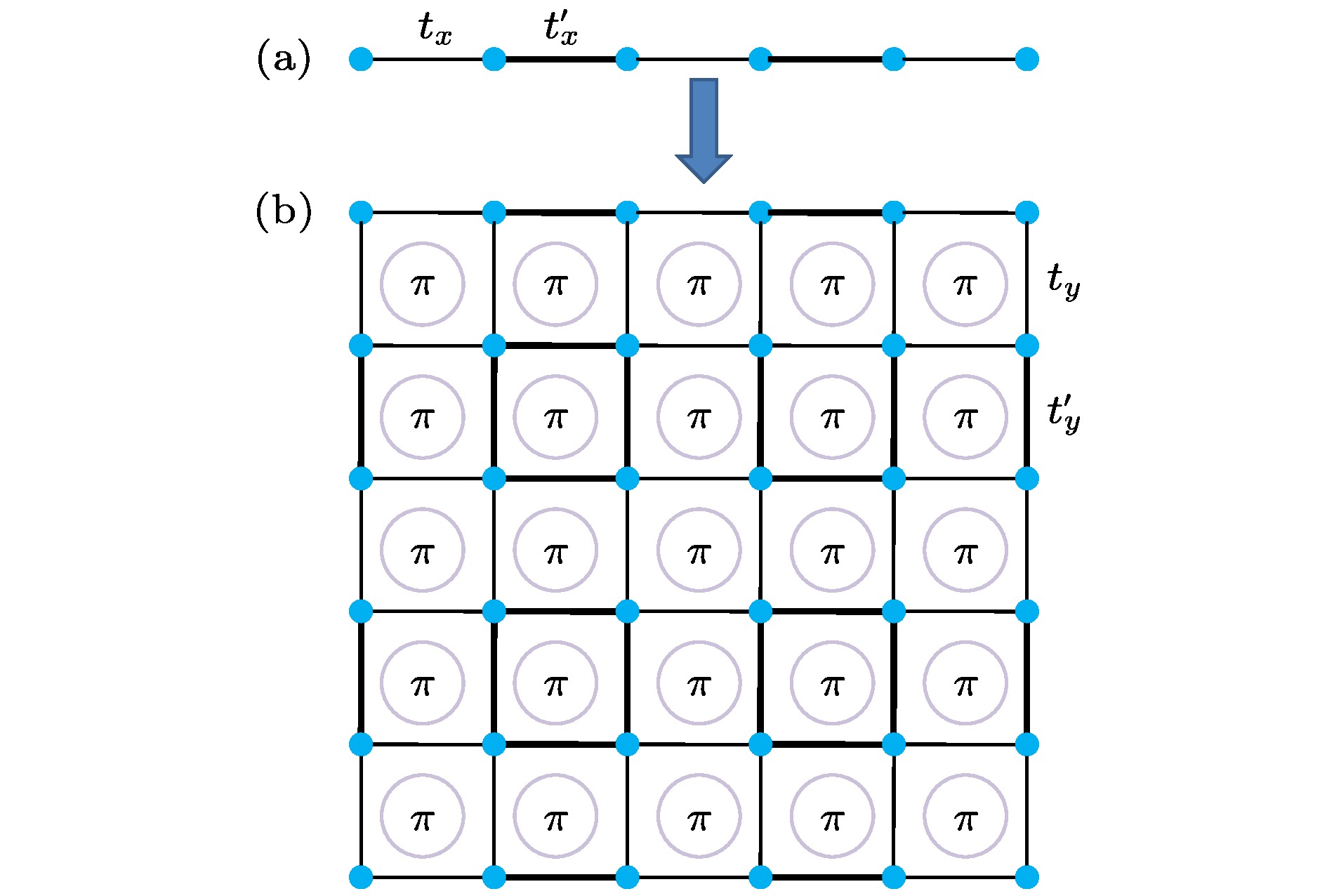 图 3 从一维一阶拓扑绝缘体到二维二阶拓扑绝缘体 (a) 一维SSH链的示意图; (b) 利用一维SSH链构造二维二阶拓扑绝缘体, 每个单位元胞中有一个


