Abstract:Vertical cavity surface emitting lasers (VCSELs) are widely used in the field of short-range optical communication and optical interconnection because of their advantages such as low threshold current, large modulation bandwidth, easy two-dimensional integration, easy coupling with optical fibers and low cost. The VCSELs and heterojunction bipolar transistor (HBT) are longitudinal current devices, so they can be well integrated on the same wafer, and the output light power can be modulated by the HBT base current. Integration of VCSELs and HBT are designed in this paper. The VCSELs and PNP InGaP/GaAs HBT form a direct series structure. The reflectivity of DBR is 99.72% at a resonant wavelength of 850 nm and 99.57% after adding HBT separately. Therefore, the addition of HBT has little influence on the reflectivity of DBR at the resonant wavelength. The electro-optical characteristics of the integrated structure are simulated by using PICS3D software. An interim collector is added into the model in order to ensure that the simulation can be carried out smoothly. Firstly, HBT is conducted and the current flows from the emitter to the interim collector. Then, the voltage across the interim collector and the N-type electrode is increased to make VCSELs conducted and the current of the transition collector drop to zero. The interim collector can be removed from the actual structure because the current is zero. The simulation results show that the current gain coefficient is 400, and the maximum modulation rate of the base current to the output light power rises up to 280 mW/mA. The maximum temperature in the active region increases with the base current increasing, and the output light power first increases and then tends to be saturated. The ac optical gain characteristics of the integrated structure is simulated by PICS3D, and the simulation result shows that cutoff frequency exceeds 1 GHz. The addition of HBT limits the modulation rate of the integrated structure, and further optimization of HBT structure parameters and geometric dimension are needed to improve the modulation rate. The integrated structure and simulation method established in this paper can also be used to integrate LED, LD, DFB or other luminescent devices with HBT. Keywords:vertical cavity surface emitting lasers/ heterojunction bipolar transistor/ opto-electronic integrated circuits
图 8 不同基极电流下输出光功率随N型电极电压的变化 Figure8. Output power varying with V1 at different base currents.
图 9 (a)基极电流为10 μA时器件内部温度分布; (b)有源区温度和输出光功率随基极电流的变化(V1 = –6 V) Figure9. (a) Temperature distribution of the device at a 10 μA base current; (b) temperature in active region and output power varying with the base current (V1 = –6 V).
本文利用PICS3D模拟了集成结构的交流光增益特性. 图10显示了基极电流为10 μA时交流光增益的模拟结果, 从图10可以看出其截至频率超过1 GHz. 单独模拟VCSEL得到其调制响应的–3 dB带宽为25 GHz, 由(8)式可知加入HBT限制了集成结构的调制速率, 需进一步优化HBT结构参数和几何尺寸来提高调制速率. 图 10 集成结构的交流光增益 Figure10. The ac power gain of integration structure.
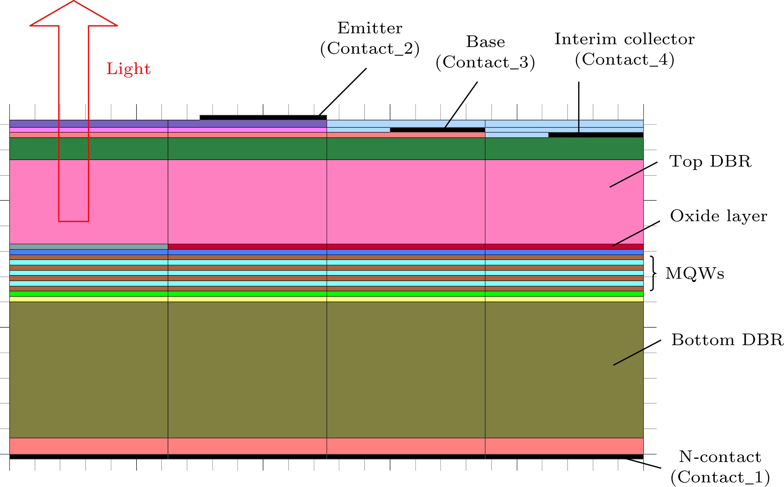 图 1 VCSELs与HBT集成结构示意图


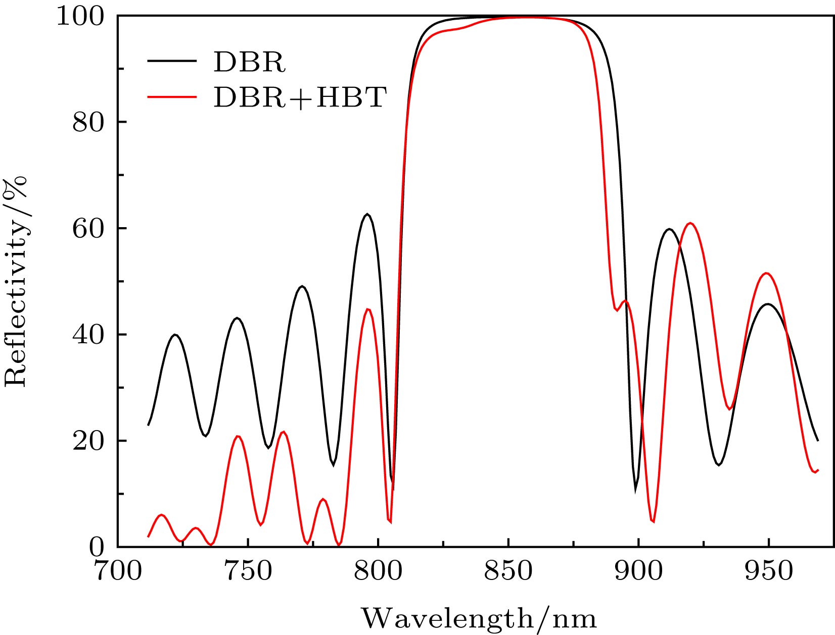 图 2 不同结构DBR反射率
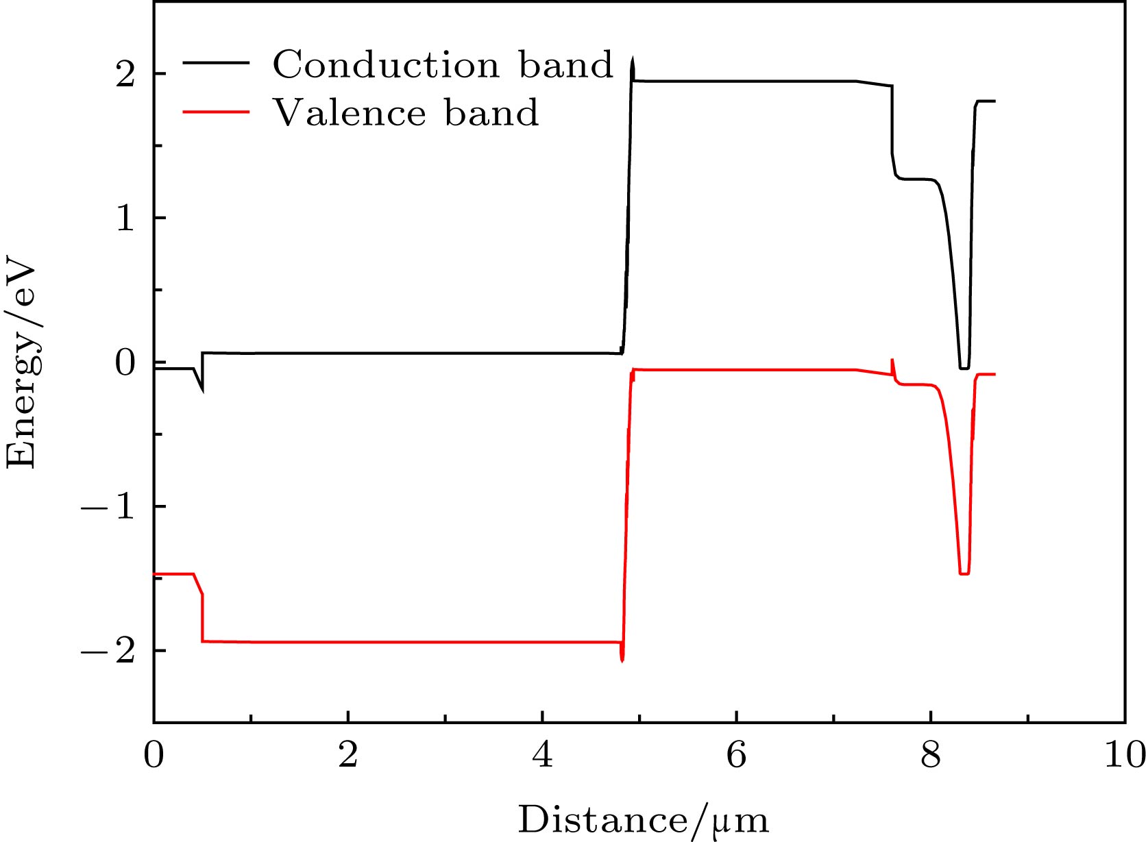 图 3 平衡态时集成结构的能带
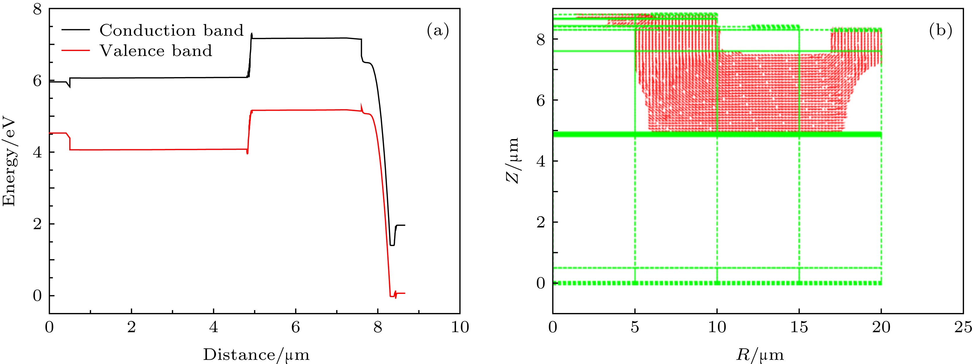 图 4 HBT处于放大状态时的(a)能带图, (b)集成结构内部电流分布
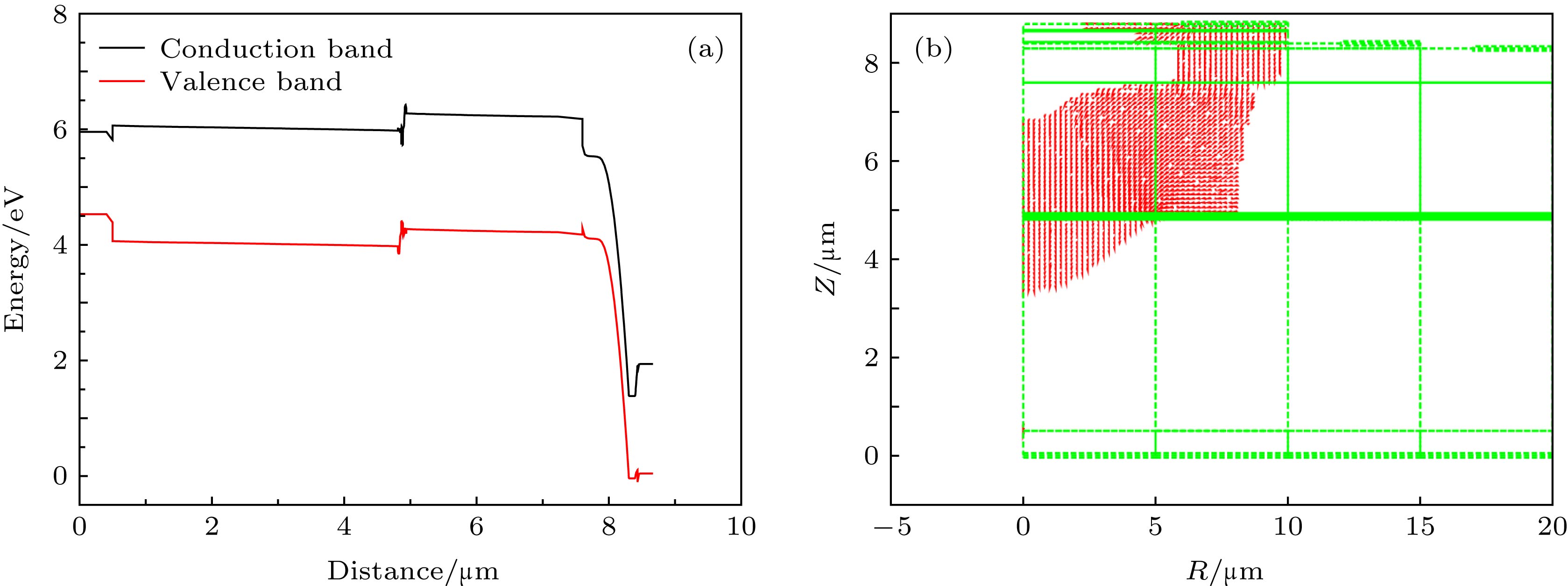 图 5 HBT和VCSEL同时导通时的集成结构 (a)能带图; (b)内部电流分布
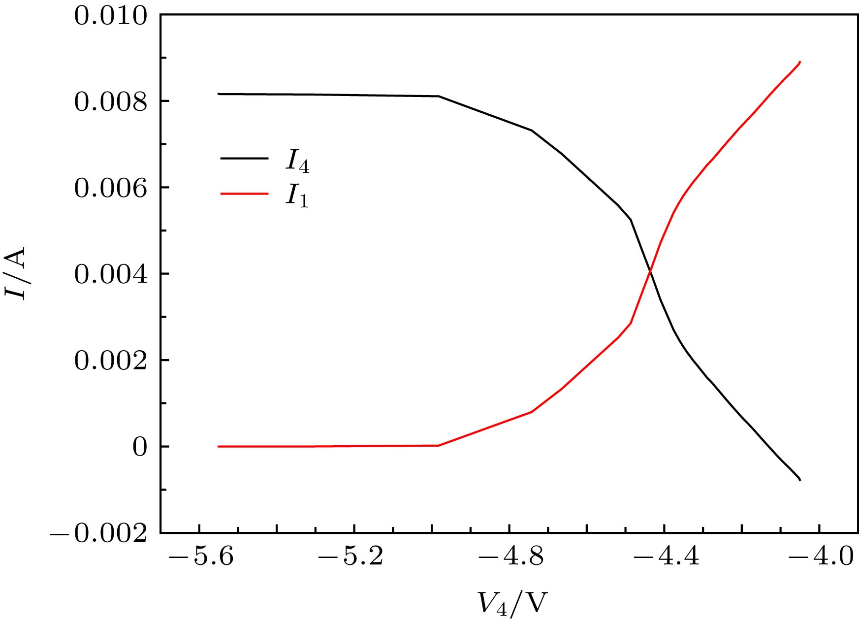 图 6 过渡集电极和N型电极电流随过渡集电极电压的变化
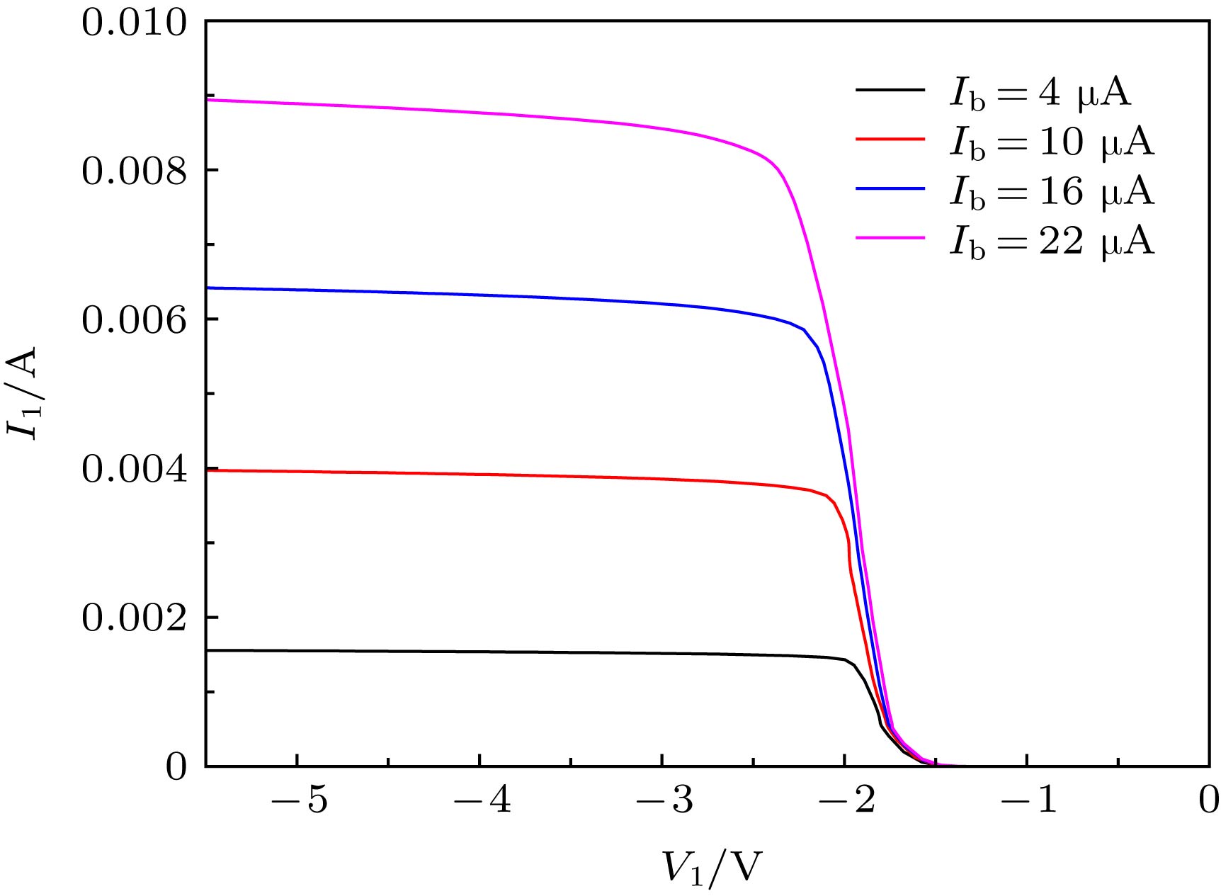 图 7 不同基极电流下N型电极电流随电压的变化
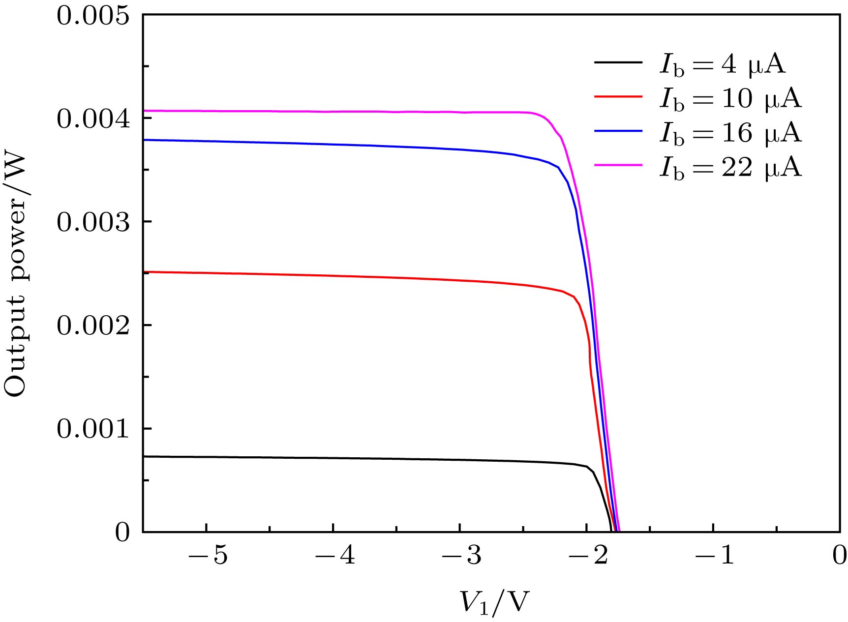 图 8 不同基极电流下输出光功率随N型电极电压的变化
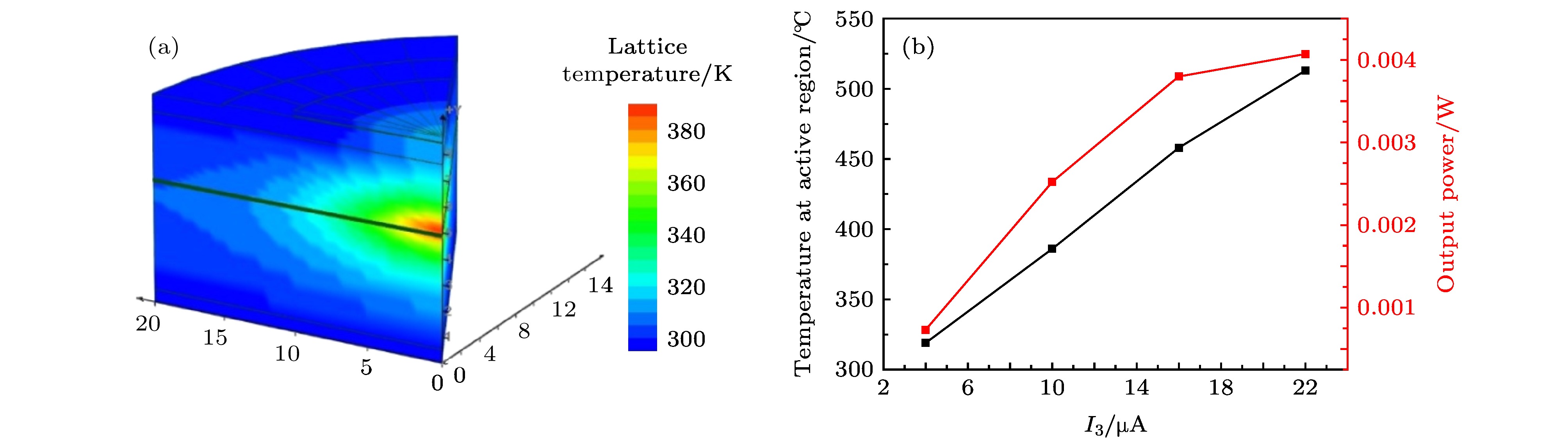 图 9 (a)基极电流为10 μA时器件内部温度分布; (b)有源区温度和输出光功率随基极电流的变化(V1 = –6 V)
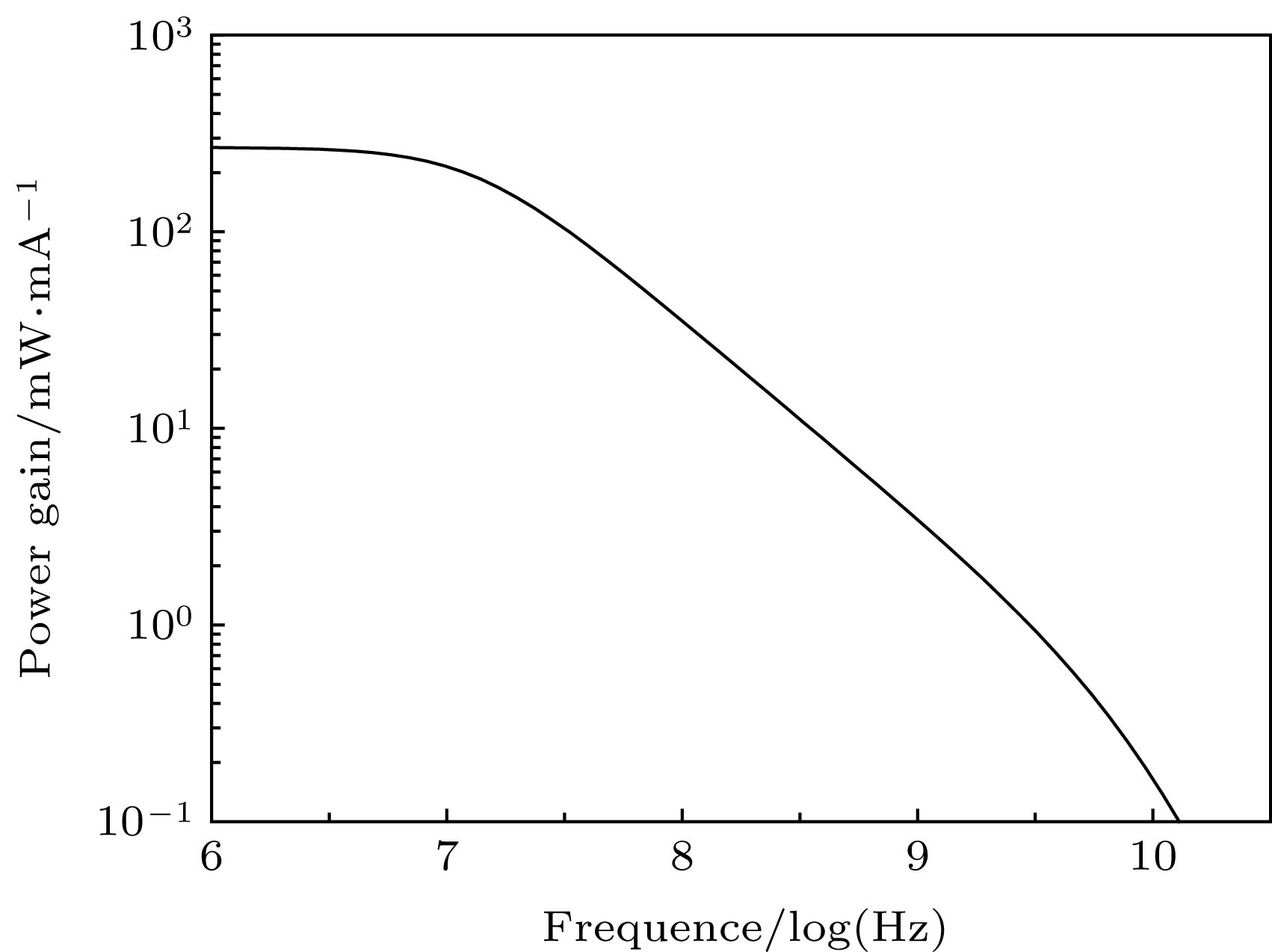 图 10 集成结构的交流光增益