全文HTML
--> --> -->目前, 人们已设计出多种基于表面等离激元Fano共振的纳米结构体系, 典型的构筑单元有棒[9,13—15]、盘(环)[16—18]和球(球壳)[19]等几类. 其中, 纳米棒由于几何结构简单、易重复制备、共振频率宽波段可调谐等特点受到了人们更多关注. Zhang等[20]首先利用“朵儿门”状的银纳米棒组合研究了Fano共振现象, 发现Fano共振来源于两平行纳米棒的电四极共振亚辐射模式和与之垂直的单纳米棒的电偶极共振超辐射模式间的相消干涉, 通过调整棒间距, 还可实现等离激元诱导透明现象. 随后, 在简单的双棒结构中也发现存在Fano共振现象, 当双棒边-边平行设置时, 其产生原因为双棒等离激元杂化形成的电偶极共振超辐射模式和磁偶极共振亚辐射模式间的电磁耦合[21,22], 或者为各个棒单独激发的电偶极辐射模式间的相消干涉[23,24]; 当双棒端-端相对设置[25]或成T型[26,27]时, 短棒的电偶极模式将通过近场耦合激发长棒的电多极亚辐射模式, 产生高阶Fano共振. 当更多纳米棒以不同的方式组合时, 纳米棒间可形成多种等离激元杂化模式, 产生双重或多重Fano共振[3,8,13,28], 使得光谱更加精细, 从而满足不同波段应用的需求.
虽然基于纳米棒组合的局域表面等离激元Fano共振受到了广泛研究, 但是由三根纳米棒平行设置构成的对称三聚体结构的Fano共振研究相对较少. 文献[24]报道了棒间距相对较大的金三聚体结构的光学性质, 指出Fano共振为中间长棒的电偶极共振和两侧边棒的电偶极共振共同作用的结果. 文献[29]分析了由中间纳米棒和两侧对称分布的U型开口环组成的类纳米棒三聚体的Fano共振特性, 阐述其产生原因为三棒电偶极共振形成的反键超辐射模式和成键反相磁偶极共振亚辐射模式间的相消干涉. 文献[30]也得到了类似的结论, 但均未就棒长度的变化对Fano共振的影响进行进一步的讨论. 本文通过时域有限差分(finite difference time domain, FDTD)方法, 研究由中间短棒和两侧长棒构成的对称金纳米棒三聚体结构的光学性质, 分析几何结构参数和介电环境对其Fano共振调谐特性的影响. 结果发现, 该纳米结构具有较强的Fano共振可调控性, 且导致Fano共振谷两侧光谱的相对强度发生改变, 共振对比度先增大后减小, 其原因在于共振峰位处电磁模式的改变.
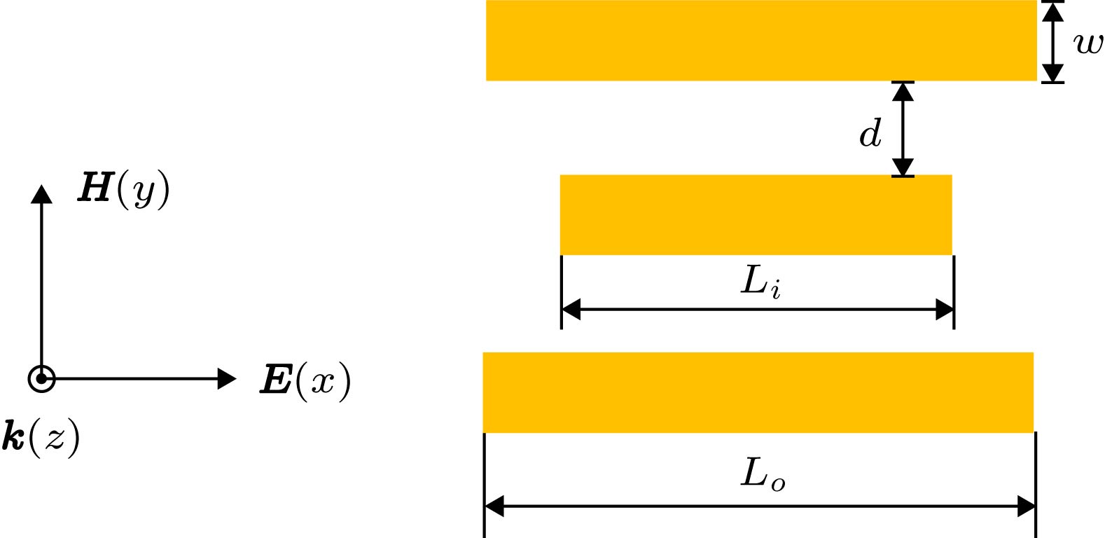 图 1 对称金纳米棒三聚体结构的模型示意图
Figure1. Geometrical structure of the symmetric Au nanorod trimer structure.
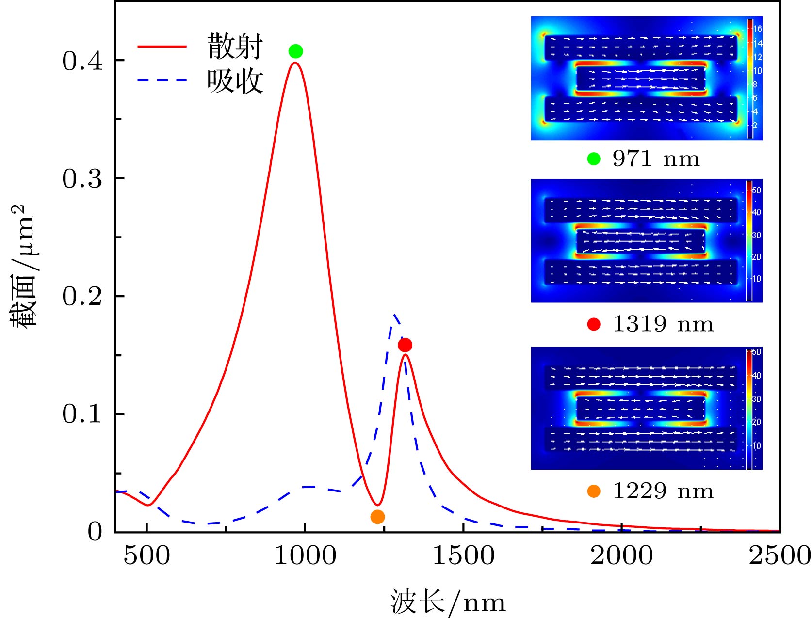 图 2 金纳米棒三聚体的散射谱和吸收谱, 插图为在两个散射共振峰位971, 1319和共振谷1229 nm处的纳米结构截面电场和电流密度矢量分布
Figure2. Scattering and absorption spectra of a single gold nanorod trimer. Insets show the calculated electric field and current density vector distributions across the central cross section of the nanorod trimer at the indicated resonances.
纳米结构的光学性质与其几何结构参数有关. 下面我们将分别改变纳米棒三聚体的相关结构参数并固定其他参数不变进行仿真对比, 进一步分析该结构的Fano共振调控性质. 图3给出了金纳米棒三聚体结构的散射谱随中间短棒长度Li变化的关系. 由图可见, 当中间短棒的长度分别为250, 200, 150和100 nm时, Fano共振谷分别处于波长1464, 1229, 1004和766 nm附近, 谷位和两侧共振峰均随短棒长度的减小而蓝移; 同时, 共振峰的强度也发生了改变, 长波处的散射强度增强, 短波处的散射强度减弱. 为了解释金纳米棒三聚体结构散射谱变化的原因, 图3插图给出了当中间短棒Li = 100 nm时两侧散射共振峰位附近的纳米结构电磁场和电流密度矢量分布. 当激发波长为716 nm时, 电场主要集中于短棒和边棒的间隙内, 与短棒内较强的同向电流密度相比, 边棒内的电流密度较小且电流密度矢量分布不同向, 边棒两端电流与短棒同相, 但中部电流却与短棒反相(见图3右上插图), 两者在间隙处形成了较强的反相磁偶极子振荡, 振荡区域约为短棒的长度(见图3右中插图); 当激发波长为1086 nm时, 在边棒的两端和三棒间隙内存在着较强的局域电场, 边棒与短棒的电流密度矢量分布反相, 但边棒的电流密度远大于短棒的电流密度(见图3右下插图). 因此, 随着中间短棒长度的减小, 短棒的电偶极共振模式对Fano共振谷长波处的成键模式影响越来越弱, 成键模式逐渐由边棒的电偶极共振模式起主导作用, 导致散射强度增大, 共振波长蓝移并逐渐接近边棒单独存在时的散射谱峰位(见图3中短点线给出的边棒对散射谱); 对于Fano共振谷短波处的共振模式, 其由反键电偶极共振超辐射模式逐渐转变成短棒主导的反相磁偶极共振模式, 使得散射强度减弱且共振频率蓝移, 从而导致Fano共振谷两侧共振峰的强度发生了转换, Fano共振对比度(spectral contrast ratio, 定义为 Fano共振处峰值和谷值之差与峰值和谷值之和的比, 即(Ipeak – Idip)/(Ipeak + Idip)[16—18])先增大后减小.
 图 3 金纳米棒三聚体的散射谱随中间短棒变化的关系, 插图为在指定频率处的纳米结构截面电磁场和电流密度矢量分布
Figure3. Scattering spectra of the nanorod trimer versus the length of center nanorod Li. Insets show the calculated electric field, magnetic field in the z-direction and current density vector distributions at the indicated resonances.
图4为当边棒的长度Lo分别为300, 400和500 nm时的纳米棒三聚体结构的散射谱. 从图中可以看出, Fano共振谷的位置基本不随边棒长度的增大而移动, 但其两侧共振峰均向长波方向移动, 且长波处的共振峰散射强度逐渐增大, 短波处的共振峰强度变化相对较小, 使得Fano共振对比度先增大后减小. 图4插图显示了当Lo = 500 nm, 激发波长分别为Fano共振谷两侧共振峰位(1143和1616 nm)时的纳米棒三聚体的电磁场和电流密度矢量分布. 当激发波长为1143 nm时, 中间短棒和边棒中部的电磁耦合产生了较强的反相磁偶极共振模式, 振荡区域约为短棒的长度, 共振频率由短棒主导. 当激发波长为1616 nm时, 边棒和中间短棒的电偶极矩振荡反向, 边棒的电偶极振荡对散射光谱的影响明显要大于短棒的作用. 因此, 随着边棒长度的增大, Fano共振谷长波处的成键模式逐渐由边棒的电偶极共振模式起主要作用, 散射强度逐渐增大和共振峰红移, 短波处的共振模式演变为由中间短棒主导的反相磁偶极亚辐射模式, 其频率基本不受边棒影响, 导致Fano共振谷的位置没有发生明显的变化.
 图 4 金纳米棒三聚体的散射谱随边棒变化的关系, 插图为在指定散射共振峰位处的纳米结构截面电磁场和电流密度矢量分布
Figure4. Scattering spectra of the nanorod trimer versus the length of side nanorod Lo. Insets show the calculated electric field, magnetic field in the z-direction and current density vector distributions at the indicated resonances.
当短棒和边棒的长度同时改变但保持长度差ΔL(Lo – Li = 100 nm)固定不变时的纳米结构散射谱如图5所示. 从图5中可以看出, 当短棒和边棒的长度同时减小时, Fano共振谷和两侧共振峰均蓝移, 且短波处的共振峰强度减弱, 长波处的共振峰强度增强, Fano共振的对比度经历了一个先增大后减小的过程. Fano共振谷蓝移的原因可能源于, 短棒和边棒的电偶极共振波长均随棒长度减小而蓝移, 从而引起成键模式和反键模式的共振波长蓝移. 为了探究强度变化的物理原因, 图5插图给出了当Lo = 200 nm, Li = 100 nm时, 在Fano共振谷两侧共振峰位683 nm和874 nm激发的纳米结构电磁场和电流密度矢量分布. 当入射波长为683 nm时, 短棒和边棒中部的电磁耦合产生了反相磁偶极共振模式, 同时, 边棒两端还存在着不可忽略的电流密度矢量分布, 其表现为在远场形成了相对较强的散射光谱. 当激发波长为874 nm时, 边棒和短棒的电流密度矢量分布反相. 可见, 随着短棒和边棒长度的同时减小, 在Fano共振短波处, 短棒和边棒中部的电磁耦合模式逐渐起主要作用, 散射强度降低; 而长波处的成键模式以边棒的电偶极共振模式为主导, 散射强度逐渐增大. 但当纳米棒的长度小到一定程度, 其等离激元共振频率靠近金材料的带间电子跃迁吸收带时, 成键模式的散射强度将减弱.
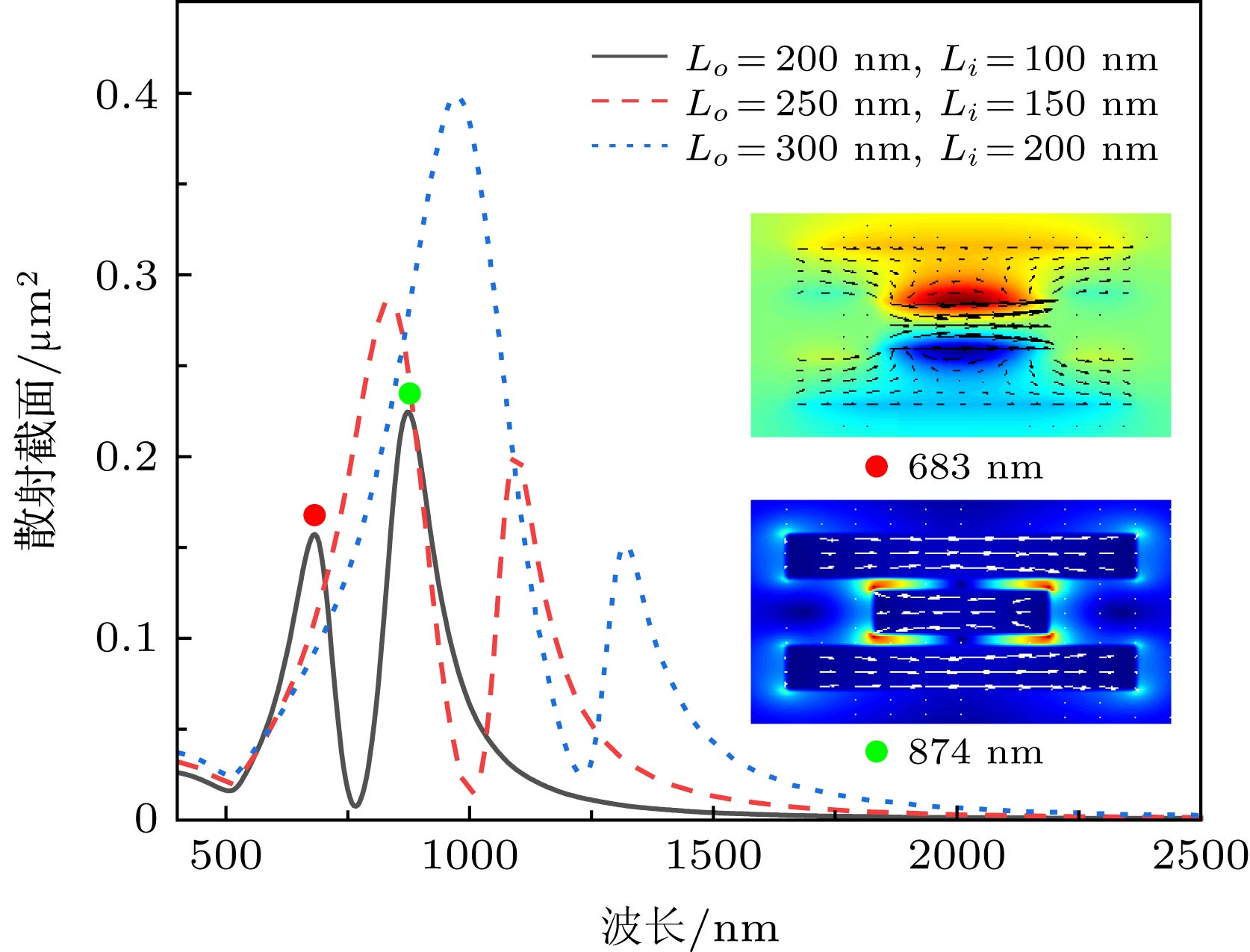 图 5 金纳米棒三聚体的散射谱随三棒尺寸变化的关系, 插图为在指定散射共振峰位处的纳米结构截面电磁场和电流密度矢量分布
Figure5. Scattering spectra of the nanorod trimer versus the nanorod length with constant displacement ΔL = 100 nm. Insets show the calculated electric field, magnetic field in the z-direction and current density vector distributions at the indicated resonances.
图6给出了当纳米棒三聚体结构的间距d分别为10, 20, 40和80 nm时的散射谱. 由图可见, 随着短棒和边棒间距的增大, Fano共振谷逐渐蓝移, 由d = 10 nm时的1229 nm移动到d = 80 nm时的905 nm, 且Fano共振谷的对比度先增大后减小, 在d = 20 nm时达到最大. 为了分析Fano共振谷蓝移的原因及两侧共振峰强度随间距变化的物理机制, 我们计算了当d = 80 nm时在Fano共振谷两侧共振峰位处的纳米结构电场和电流密度矢量分布, 如图6插图所示. 可见, 当激发波长为816 nm时, 中间短棒两端产生很强的局域电场, 形成电偶极共振模式, 而两侧边棒产生的电场很弱, 几乎没有激发出电偶极共振模式, 同时短棒和边棒之间的近场耦合作用很弱, 此时的模式可表示为短棒主导的电偶极共振辐射模式; 当激发波长为1084 nm时, 此时电场主要集中于边棒的两端, 而短棒的电流密度矢量分布虽然与边棒反相, 但其作用可忽略不计, 此时激发的模式可表示为边棒主导的电偶极共振辐射模式. 因此, 随着棒间距的增大, 短棒和边棒之间的近场耦合效应减弱, 反键模式和成键模式分别退化为短棒和边棒的电偶极共振模式, 两者相消干涉形成Fano共振[24], 且由于边棒的辐射强度大于短棒的辐射强度, 其共振波长也大于短棒的共振波长, 导致长波处的共振强度增大, 短波处的共振强度减弱.
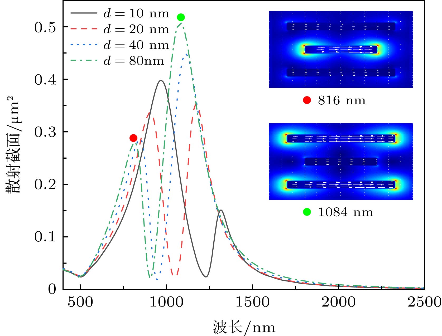 图 6 金纳米棒三聚体的散射谱随棒间距变化的关系, 插图为在指定散射共振峰位处的纳米结构截面电场和电流密度矢量分布
Figure6. Scattering spectra of the nanorod trimer versus inter-rod spacing d. Insets show the calculated electric field and current density vector distributions at the indicated resonances.
Fano共振不仅与纳米结构的几何参数有关, 还与纳米结构周围的介电环境有关. 图7给出了仅当短棒与边棒的间隙内介电环境改变时, 纳米棒三聚体的散射谱与介质折射率的关系. 其中, 短棒的长度Li取为100 nm, 填充介质的折射率从1取到2.5, 其他结构参数固定不变. 从图7中可以看出, 随着间隙内介质折射率的增大, Fano共振谷红移, 两侧共振峰的相对强度发生了转换, Fano共振对比度明显先增大后减小. Fano共振谷红移可能是因为, 随着短棒两侧介质折射率的增大, 介质内的极化电荷增多, 使得短棒两端电荷的库仑回复力减小, 电偶极共振波长增大, 导致两侧共振峰位均红移. 另一方面, LC谐振电路指出, 共振波长与成正比[35], 而电容又与棒间介质的介电函数有关. 因此, 共振波长与介质折射率约成正比, 随介质折射率的增大而增大. 而共振峰强度的变化, 我们可以从图7插图分析得到. 该插图为当填充介质折射率为2.5, 激发波长分别为共振峰位1017 nm和1395 nm时的纳米结构电磁场和电流密度矢量分布. 可见, 此时Fano共振谷短波处的共振表现为电偶极共振超辐射模式, 光谱强度较大, 而长波处的共振主要以反相磁偶极共振亚辐射模式为主, 光谱较弱.
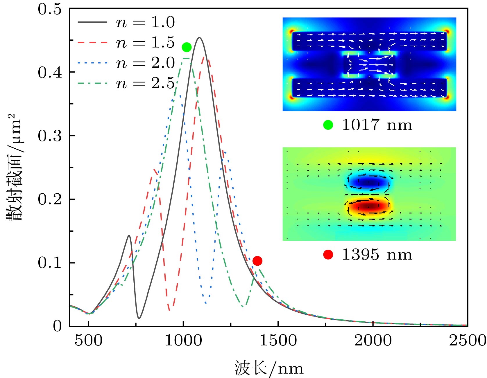 图 7 当短棒与边棒的间隙内介电环境变化时, 金纳米棒三聚体的散射谱随介质折射率变化的关系, 插图为在两个散射共振峰位处的纳米结构截面电磁场和电流密度矢量分布
Figure7. Scattering spectra of the nanorod trimer with different media in the gaps between the center and side nanorods. Insets show the calculated electric field, magnetic field in the z-direction and current density vector distributions at the indicated resonances.
此外, 当纳米棒三聚体结构的空间对称性被打破, 如短棒和两侧边棒的间距不同, 或两侧边棒的长度不等时, 将可能导致上下间隙内的反相磁偶极共振模式的频率不再相同[29]或模式的分裂[36], 激发出双重Fano共振, 导致光谱更加精细.
