1.School of Computer Science and Telecommunication Engineering, Jiangsu University, Zhenjiang 212013, China 2.Jiangsu Key Laboratory of Security Tech. for Industrial Cyberspace, Jiangsu University, Zhenjiang 212013, China
Fund Project:Project supported by Jiangsu Key laboratory of Security Tech. for Industrial Cyberspace, China (Grant No. STICB201906)
Received Date:22 May 2019
Accepted Date:08 July 2019
Available Online:01 October 2019
Published Online:05 October 2019
Abstract:In order to solve the technical problem of the traditional electric field sensor limited by its measurement range, a parity-time (PT) symmetric microcavity structure doped by electro-optical medium is designed, and a new electric field sensing mechanism is proposed. The transfer matrix method is used to calculate the transmission spectrum of the structure. A unique amplified defect mode is found. The peak value and wavelength position of the defect mode vary with the external electric field. The same electric field can be measured by using two mechanisms. One is to detect the change of the defect mode peak value, and the other is to measure the change of the defect mode wavelength position. The measurement range is limited only by the breakdown field value of the electro-optical medium, which can range from 0 to 0.06 V/nm, covering almost any possible electric field environment. For the peak-value sensing mechanism, the sensitivity range is 38.042—47.558 (nm/V); for the wavelength position sensing mechanism, the sensitivity range is 18.357—18.642 (nm2/V), and the average resolution in the measurement range is 0.00925 V/nm. Keywords:electric field sensor/ parity-time symmetry structure/ defect mode
图 4 不同dB下的缺陷模式的峰值位置变化 Figure4. The positions of defect modes with different dB.
结构的周期数N是影响透射峰值的重要因素, 因此需要研究N对总体结构放大作用的影响. 首先不施加电场, 即Eex = 0, 任取$N = 5$并画出结构的透射率谱线, 结果如图5(a)所示. 从图中可以看到该结构在1500—1607 nm之间存在一个禁带, 而在1550.5 nm附近出现在了一个缺陷模式, 缺陷模式主要是由中间缺陷共振腔引起的, 在缺陷模式处的透射率大于1, 达到了2.312, 说明在该模式下结构对入射光产生了放大作用. 在缺陷模式对应的波长处, 整体结构近似满足PT对称条件, 由此可知入射光的放大作用是由PT对称引起的. 图5(b)和图5(c)分别给出了N = 6, 7时结构的透射率谱线, 结构周期数N不同, 共振腔的透射峰峰值也不同, 分别在1550.44和 1550.4 nm处为 15.803, 2.274. 显然, N = 6时结构对入射光的放大作用最强, 所以结构的透射率并不是随周期数目单调增加的. 本文的缺陷模式与一般光子晶体的缺陷模式不同. 一般光子晶体的缺陷模式透射率小于或等于1, 且对周期数的变化依赖很小. 但在本文PT对称结构中, 虽然增益介质层和损耗介质层在结构中的分布是均匀的, 但入射光在结构中所受的衰减或增益不一定是平衡的. 入射光在不同介质层中的群速度存在差异. 当入射光在增益介质层(C层)中的群速度低于衰减介质层(A层)时, 光子与增益介质相互作用的时间更长. 外部的泵浦能量通过增益介质转化为电磁能量[19], 结构整体就表现出放大作用. 另外, 结构中除了微腔D层, 每个B层也可以看成局部微腔, 整体结构是一个耦合共振系统. 在特定频率, 局部微腔和整体结构发生耦合共振, 此时增益介质层和损耗介质层之间发生能量交换的同时, 从外界泵浦吸收更多的能量, 转化为电磁能量, 整体结构就会产生很大的增益传输. 这种耦合共振的条件无疑与结构周期数目有关, 显然在本文中N = 6耦合共振效应最强. 为了使得本文设计的传感器达到尽可能高的灵敏度, 在之后的计算中均选取N = 6. 图 5 周期数不同时的结构透射谱 (a) N = 5; (b) N = 6; (c) N = 7 Figure5. The transmission spectra of the structure with different period number: (a) N = 5; (b) N = 6; (c) N = 7.
以上结果是在完全满足PT对称构型的条件下取得的. 为了显示PT对称构型的特征, 在图5(b)的基础上改变${{\omega }_0}$的取值, 令${{\omega }_0} = \dfrac{{2{\text{π}} \rm{c} }}{{1500\;\rm{nm} }}$, 把计算的传输谱与图5(b)进行比较, 结果如图6所示. 在1550 nm附近处, 图5(b)中${{\omega }_0} = \dfrac{{2{\text{π}} \rm{c} }}{{1550\;\rm{nm} }}$满足PT对称构型, 出现较大的透射峰; 而取${{\omega }_0} = $$\dfrac{{2{\text{π}} \rm{c} }}{{1500\;\rm{nm} }}$导致偏离PT对称构型, 透射峰值小于4, 大幅下降. 图 6 两种${{\omega }_0}$的取值得到的传输谱 Figure6. The transmission spectra of the structure with two values of ${{\omega }_0}$.
为了理解缺陷模增益传输的物理本质, 以及验证计算结果的可靠性, 分别根据传输矩阵方法编程计算和comsol软件频域仿真来画出针对N = 6缺陷模在结构内部对应的场分布, 入射电场大小均为为1 V/m, 结果如图7所示. 可以明显看出每一层的局域驻波共振和整体结构的谐振效应. 场在中间三层达到最大值, 且A, C层场值总是大于相邻的B, D层场值. 耦合共振效应让增益层从外界泵浦吸收能量变成电磁波能量, 导致透射率大于1. 传输矩阵方法编程计算和基于有限元方法的comsol软件频域仿真结果在场的大小和分布上完美一致, 计算方法得到验证. 图 7 两种方法研究结构周期数N = 6时缺陷模在结构内部对应的场分布 (a) 传输矩阵方法; (b) comsol软件频域仿真 Figure7. The field distributions inside the structure with N = 6: (a) Calculation based on the transfer matrix method; (b) frequency domain simulation based on Comsol.
图 11 (a)缺陷模波长与电场的变化关系; (b)灵敏度分布 Figure11. (a) The wavelength of defect mode versus the electric field; (b) the sensor sensitivity.
传感器的分辨率表示的是传感器能够分辨的最小电场${E_{{\rm{ex}}}}$的变化量. 这个变化量越小, 传感器的分辨率就越高. 如果以透射峰波长位置表示${E_{{\rm{ex}}}}$大小, 就可以使用透射峰位移来计算分辨率. 图12给出了缺陷模透射峰波长间隔正好大于半角带宽的两个缺陷模分布, 此时每个子图中两个缺陷模对应场强的差值就是该处测量能够分辨的最小电场变化量, 即分辨率. 从计算结果可以看出, 在整个测量范围分辨率变化很小, 因此可用平均分辨率表示, 经过计算得平均分辨率为0.0095 V/nm. 图 12 传感器分辨率的确定, 图中标注峰值间隔等于峰的半角宽度 Figure12. The determination of resolution. The interval of two peaks is just equal to the half-angular breadth.


 图 1 结构示意图


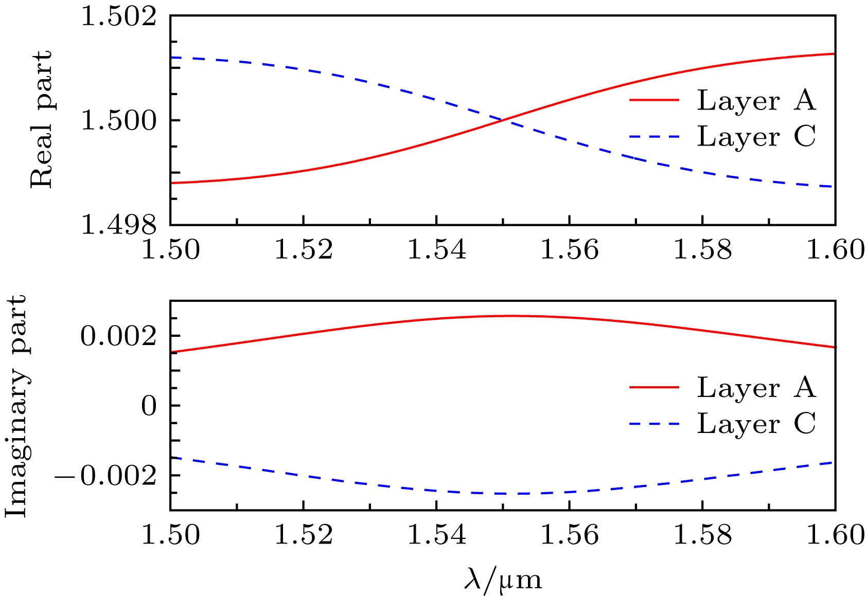 图 2 A, C层的介电常数的实部和虚部随波长的分布


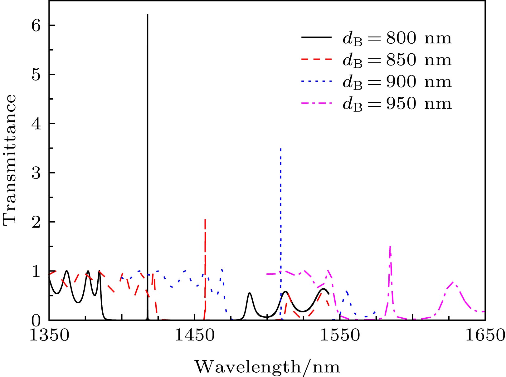 图 3 不同dB下的结构透射率谱线
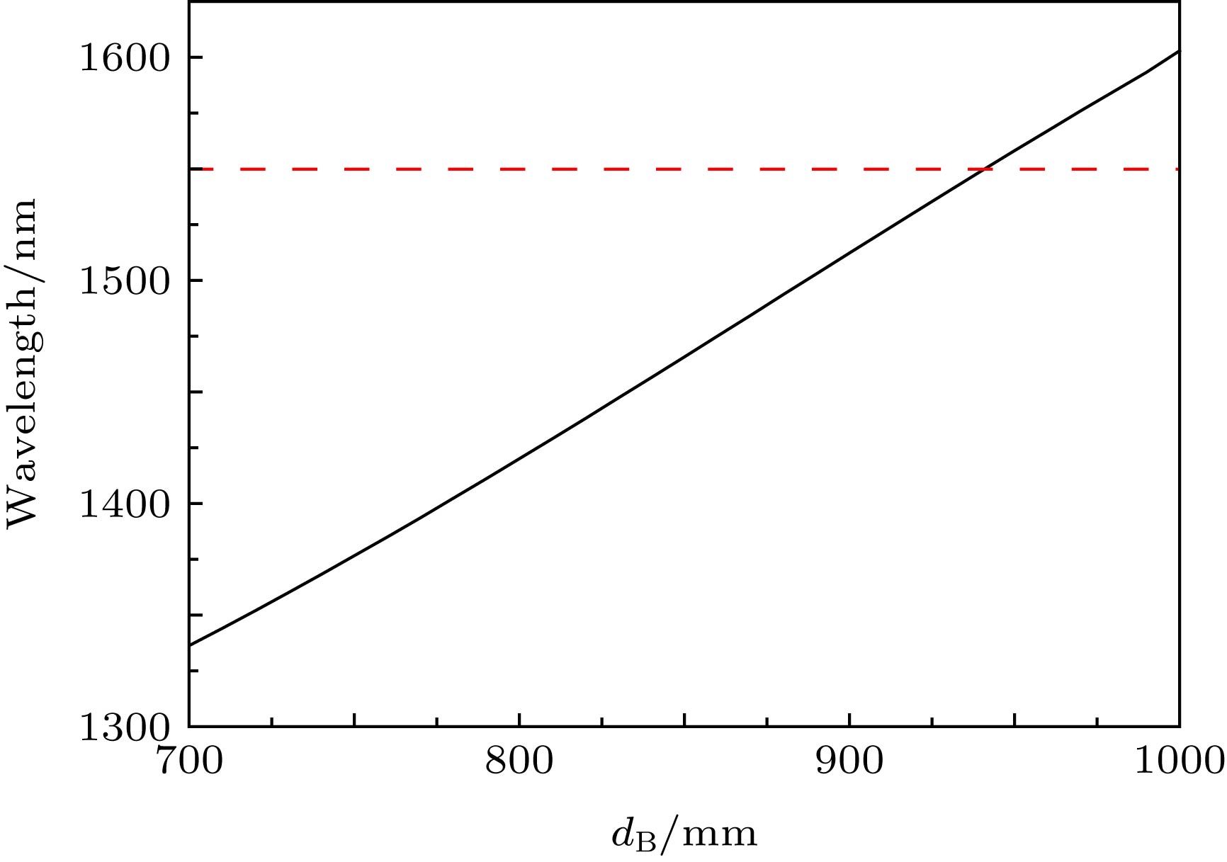 图 4 不同dB下的缺陷模式的峰值位置变化
 图 5 周期数不同时的结构透射谱 (a) N = 5; (b) N = 6; (c) N = 7


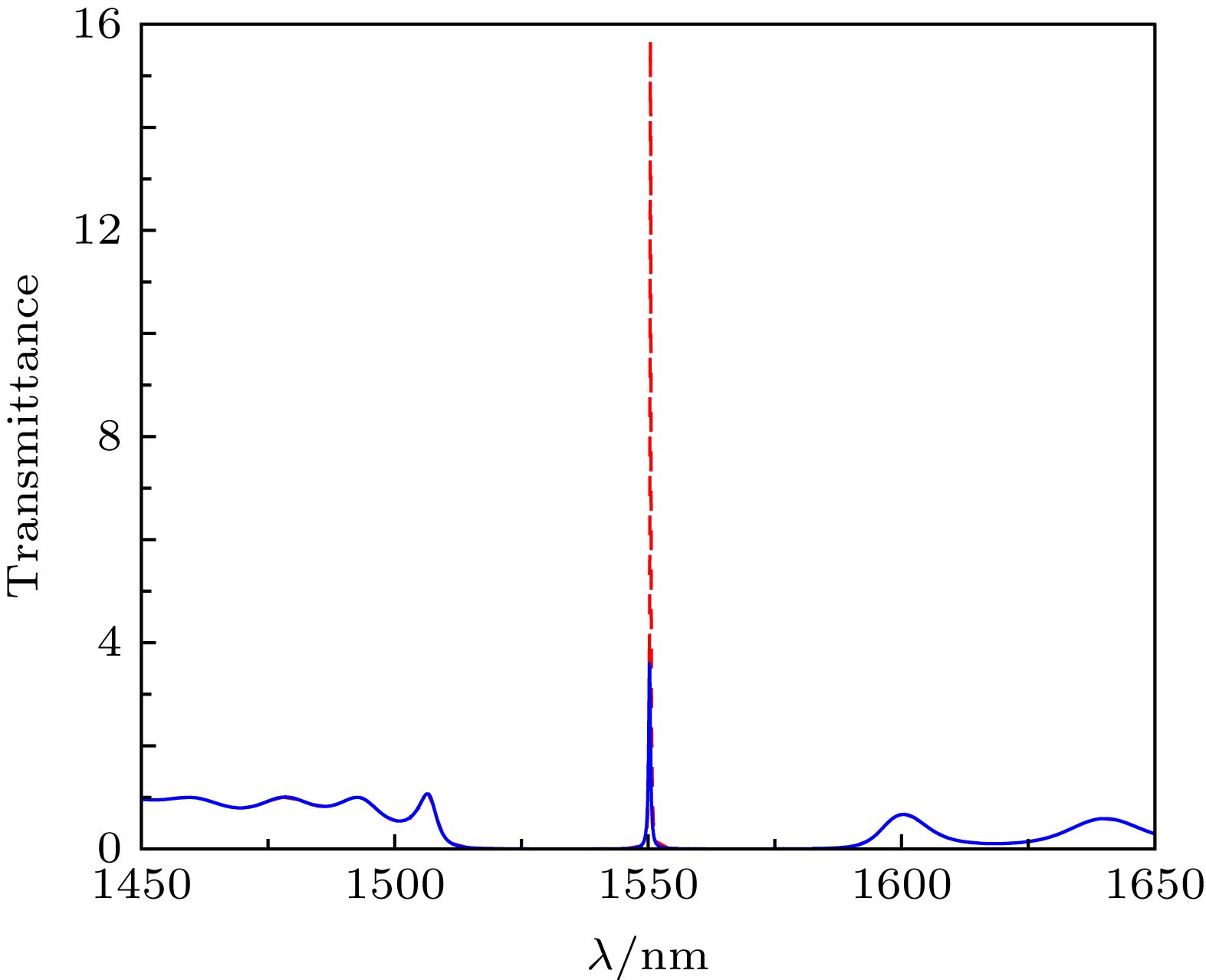 图 6 两种

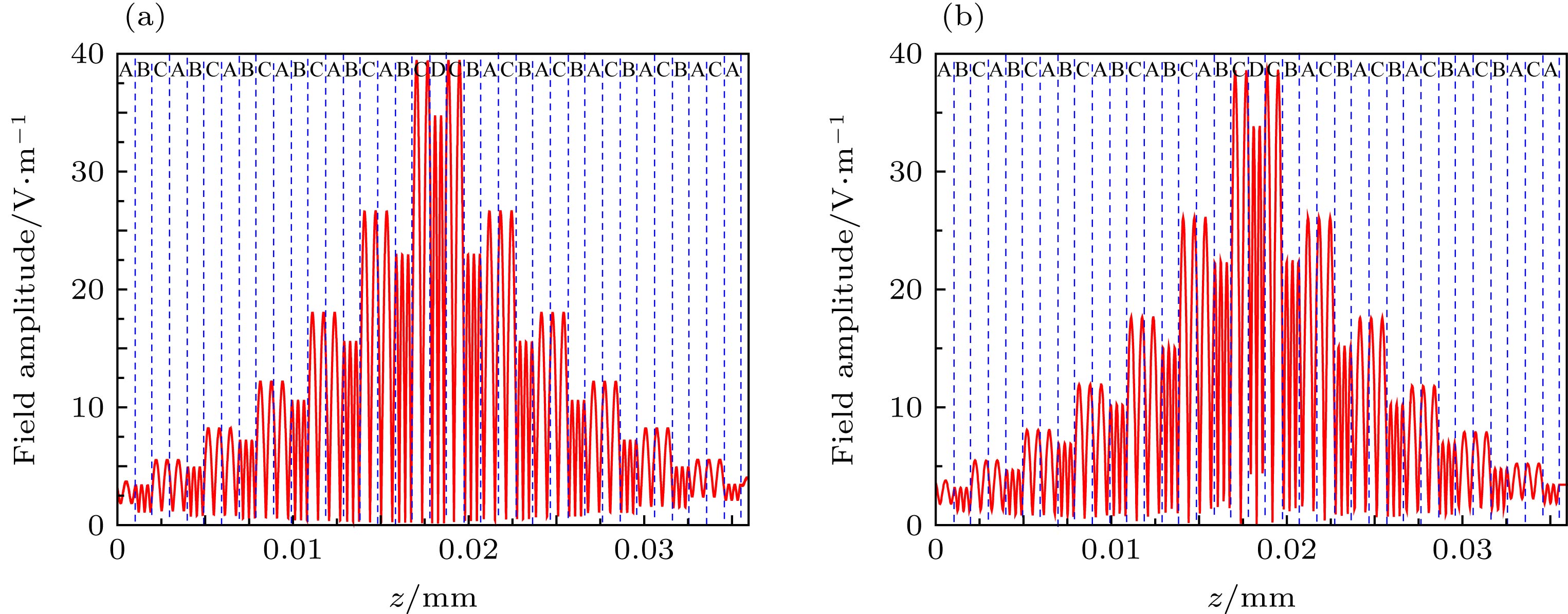 图 7 两种方法研究结构周期数N = 6时缺陷模在结构内部对应的场分布 (a) 传输矩阵方法; (b) comsol软件频域仿真
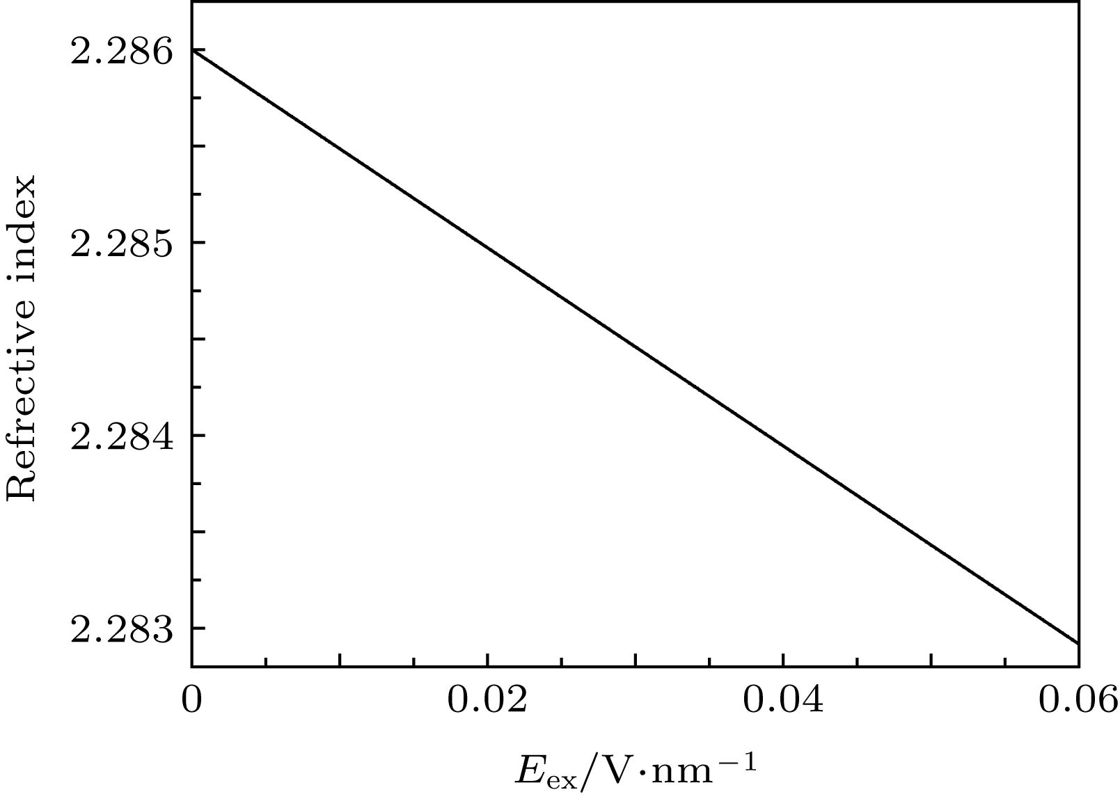 图 8 LiNbO3的折射率与电场的关系
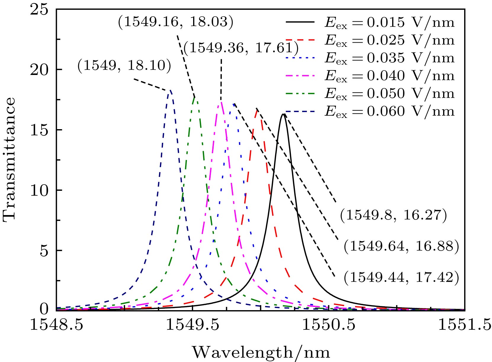 图 9 不同电场条件下结构共振腔的透射谱
 图 10 (a)缺陷模峰值大小与电场的变化关系; (b)传感灵敏度
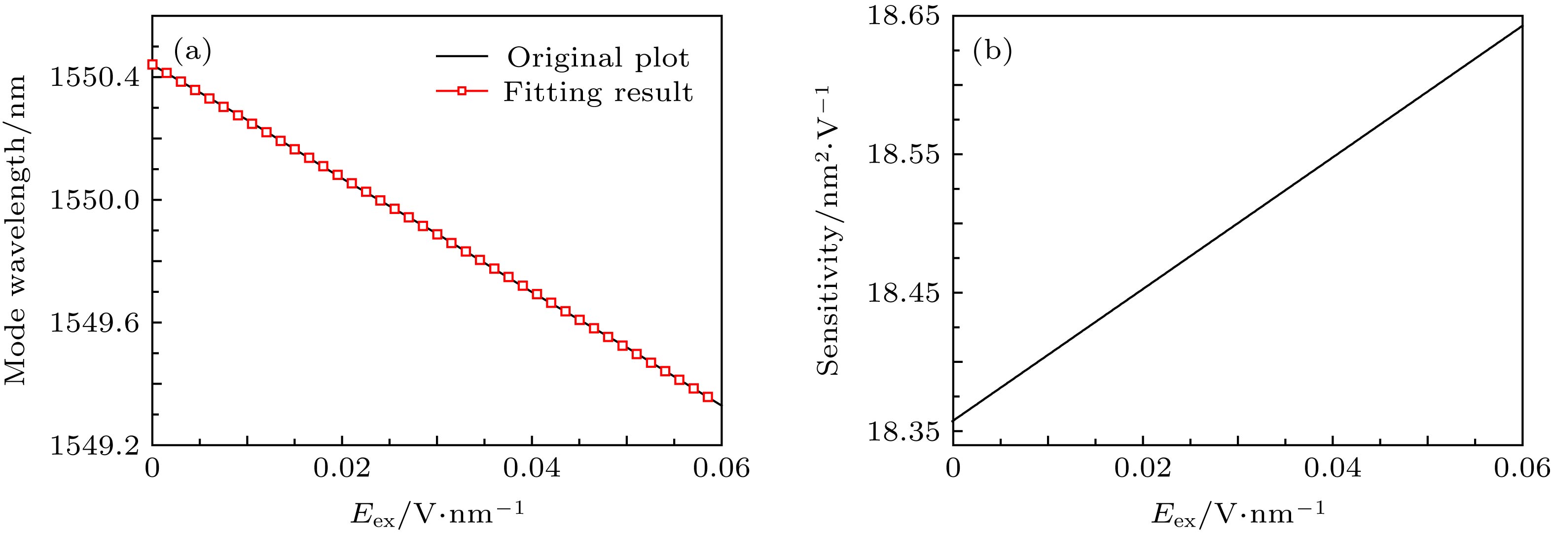 图 11 (a)缺陷模波长与电场的变化关系; (b)灵敏度分布

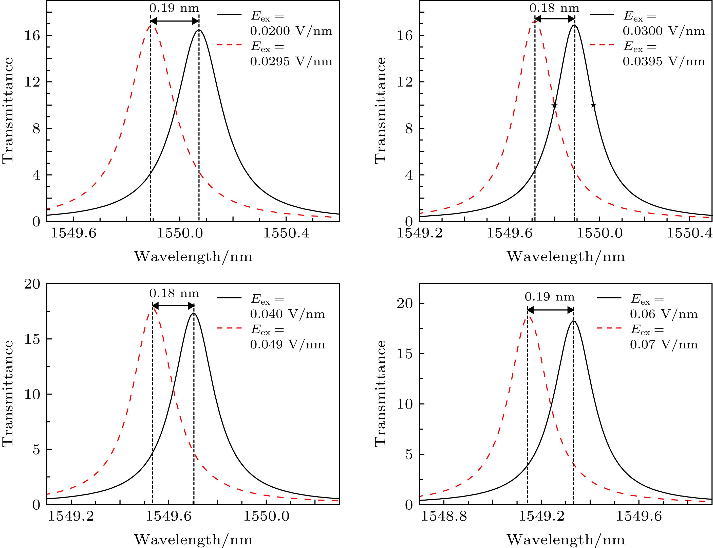 图 12 传感器分辨率的确定, 图中标注峰值间隔等于峰的半角宽度


 图 13 不同

