1.School of Physics and Electronics, Central South University, Changsha 410083, China 2.School of Physics and Electronics, Hunan Normal University, Changsha 410006, China
Fund Project:Project supported by the National Key Research and Development Program of China (Grant No. 2017YFA0204600) and the National Natural Science Foundation of China (Grant No. 51802352).
Received Date:10 April 2019
Accepted Date:12 July 2019
Available Online:01 September 2019
Published Online:20 September 2019
Abstract:Graphene is an ideal two-dimensional crystal with the advantages of high conductivity, unique physical and chemical properties, and high specific surface area. Especially, because of its super excellent electronic properties, graphene may substitute the traditional semiconductor silicon material and carbon nanotube, thus creating a new nanoscale electronic device. In addition, multilayer graphene with ultra-wide spectral absorption characteristics and unique photoelectric properties is an ideal material for photovoltaic devices. However, the zero band gap and semi-metality of graphene both limit its application in space detectors such as the microelectronic industries and satellites. Opening and regulating the graphene band gap by physical methods has become one of the key means to further expand its applications. Research work has shown that the doping of elements can significantly change the electronic structure of graphene, thereby regulating the optical properties of graphene. In order to provide an insight into electronic properties of graphene and tune its electronic band structure and optical properties effectively, electronic and optical properties of Ni-doped multi-layer graphene are studied and a number of interesting results are obtained. The calculation are carried out by the CASTEP tool in Materials Studio software based on the first-principles of ultrasoft pseudopotential of density functional theory. The models of three typical doping positions relative to carbon atoms are constructed. After structural optimization, it is obtained that " above the center of two carbon atoms” is the most stable doping structure. By using the method of local density approximation, the band structure, density of states, dielectric constant, reflectivity and refractive index of the models are calculated. The results show that an enhanced energy band gap can be achieved after nickel-doping, and reach up to 0.604 eV. Besides, peaked phenomenon of density of states at Femi level can be observed, which is accomplished by enhancing the plasma energy. Furthermore, the calculations show that the imaginary part of permittivity and refractive index increase after nickel-doping, suggesting that the optical absorbing performance is improved. All these results provide theoretical guidance for further exploring the optical properties of graphene. Keywords:graphene/ first principle/ Ni-doping/ electronic structure/ optical properties
全文HTML
--> --> --> 1.引 言自2004年英国曼彻斯特大学的Geim和Novoselov[1,2]用机械剥离法成功获得石墨烯以来, 掀起了石墨烯的研究热潮[3—5]. 石墨烯具有高比表面积、高导电性及优异的力学、热学性能, 可广泛应用于新型锂电池负极材料、超级电容电极材料[6]、显示电子器件[7]和半导体器件[8]等领域. 然而, 作为一类综合性能优异的碳纳米材料, 石墨烯自身的光吸收性能不佳, 单层石墨烯的吸光率仅为2.3%; 但随着层数增多, 多层石墨烯的吸光率呈增大趋势[9]. 研究发现, 具有超宽光谱吸收特性及独特光电性能的多层石墨烯是制作光电器件的理想材料. 然而石墨烯的零带隙半金属性限制了其在微电子工业和卫星等太空探测器领域的应用, 通过物理化学方法打开和调控石墨烯带隙成为进一步拓展其广泛应用的关键手段之一. Schedin等[10]通过在石墨烯表面吸附气体分子, 测试分析了带隙大小与载流子浓度和电阻变化率的关系, 研制的石墨烯探测器有望应用于机敏探头等. Reddy等[11]利用化学气相沉积法研究了氮掺杂石墨烯层的受控生长, 结果表明这种方法制得的石墨烯可逆电容量是本征石墨烯可逆电容量的两倍. 文献[12—14]将B, N, Al等元素掺入石墨烯及碳纳米管, 发现掺入杂质元素可改变其结构特性和化学敏感度. 已有研究工作[15,16]表明, 通过元素掺杂可以显著改变石墨烯电子结构, 从而调控石墨烯的光学特性. 晶格常数匹配性是保障掺杂体系稳定的前提. 过渡金属元素镍的晶格常数与石墨烯的晶格常数(2.46 ?)较为匹配, 且石墨烯本身为半金属性, 掺杂镍不会显著改变石墨烯的结构. 此外, 双层石墨烯的费米能级附近的两支能带有分离的趋势, 有可能会因外界原子的引入对费米能级附近的色散关系产生重要影响[17]. 本文选用镍原子对双层石墨烯和三层石墨烯进行层间掺杂, 以期打开石墨烯的带隙, 提高其吸光性能. 以AB型双层石墨烯和ABA型三层石墨烯为研究对象, 探讨镍元素掺杂对多层石墨烯体系的能带、态密度(DOS)和光吸收系数的影响规律及作用机理. 2.计算方法采用基于密度泛函理论平面波赝势方法的Materials Studio软件的CASTEP模块, 优化几何结构和计算电子结构. 利用局域密度近似处理电子间相互作用的交换关联能. 平面波截断能设置为800 eV, 在结构优化中, 自洽收敛值取1.0 × 10⁻⁶ eV/atom, 总能量收敛小于1.0 × 10⁻⁵ eV/atom. 最大Hellmann-Feynman力取为0.03 eV/?, 最大应力小于0.05 GPa. 最大原子位移小于1 × 10⁻³ ?, Brillouin区的K点采用Monkorst-Park空间网格取法. 对于多层石墨烯掺杂前后的结构优化采用11 × 11 × 1的K点, DOS及光学特性相关计算采用21 × 21 × 1的K点. 为消除石墨烯双层与双层之间沿Z方向产生的相互作用, 晶体模型的真空层厚度选为20 ?. 图1(a)和图1(b)分别是镍原子掺杂的双层石墨烯原胞模型的俯视图和侧视图, 模型采用2 × 2超胞AB堆垛的双层石墨烯, 超胞晶格常数设置为a = b = 4.92 ?, 双层石墨烯结构优化后的晶格参数为a = b = 4.884 ?, 与文献[18, 19]中双层石墨烯的晶格参数极为接近. 图 1 镍原子掺杂的双层石墨烯的(a)俯视图和(b)侧视图; 镍原子掺杂的三层石墨烯的(c)俯视图和(d)侧视图(蓝色代表石墨烯, 绿色代表镍原子) Figure1. (a) Top view and (b) side view of bilayer graphene cell (marked as blue) doped with nickel (marked as green); (c) top view and (d) side view of trilayer graphene cell (marked as blue) doped with nickel (marked as green).
由(3)和(4)式可知, 吸收系数与消光系数成正比, 如图5所示, 在可见光波段(390—760 nm), 掺杂镍原子的双层石墨烯的折射率虚部(消光系数)比掺杂之前的高, 表明损耗大, 吸光性能好. 图 5 双层石墨烯掺杂前后的折射率与波长的关系 Figure5. Refractive index versus wavelength for the Ni-doped bilayer graphene and pure bilayer graphene.
由图6可知, 相同层数的石墨烯体系, 相比本征石墨烯, 掺杂镍原子的石墨烯其反射率R有所降低. 掺杂之后的双层石墨烯在可见光波段的反射率都低于0.1, 掺杂之后的三层石墨烯在可见光波段的反射率都低于0.15, 即镍原子的层间掺杂有效降低了石墨烯的反射率. 本征石墨烯[26]随着层数的增加, 透射率T依次下降2.3%, 进行层间掺杂后透射率下降更快, 且计算证明镍原子掺杂能有效降低石墨烯体系的反射率, 故由$ A + R + T = 1$可知, 镍原子的层间掺杂能有效提升石墨烯的吸光性能. 图 6 掺杂前后的单层、双层和三层石墨烯的反射率 Figure6. Comparison of reflectivity of monolayer, bilayer and trilayer graphene with and without Ni doping.
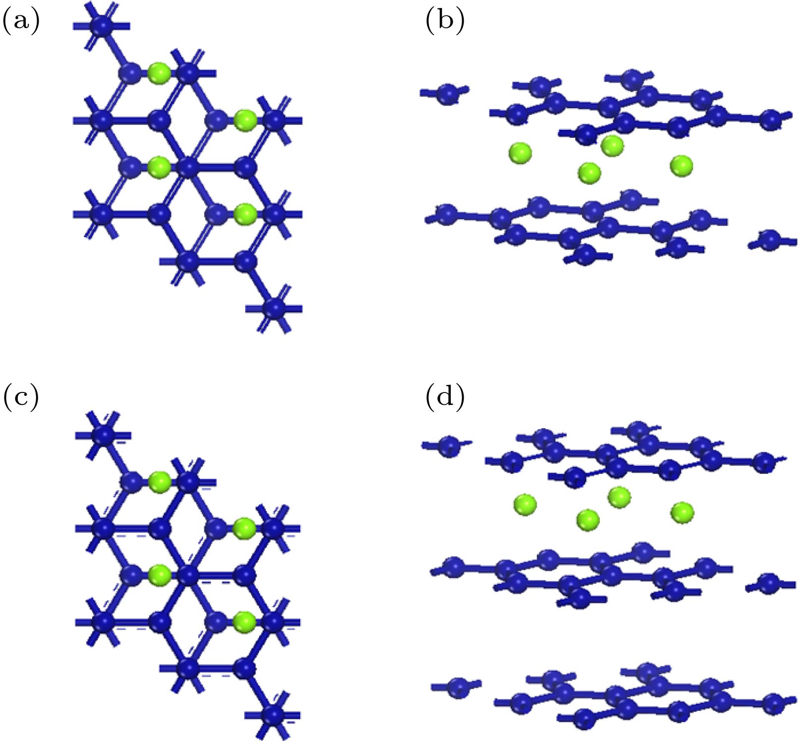 图 1 镍原子掺杂的双层石墨烯的(a)俯视图和(b)侧视图; 镍原子掺杂的三层石墨烯的(c)俯视图和(d)侧视图(蓝色代表石墨烯, 绿色代表镍原子)
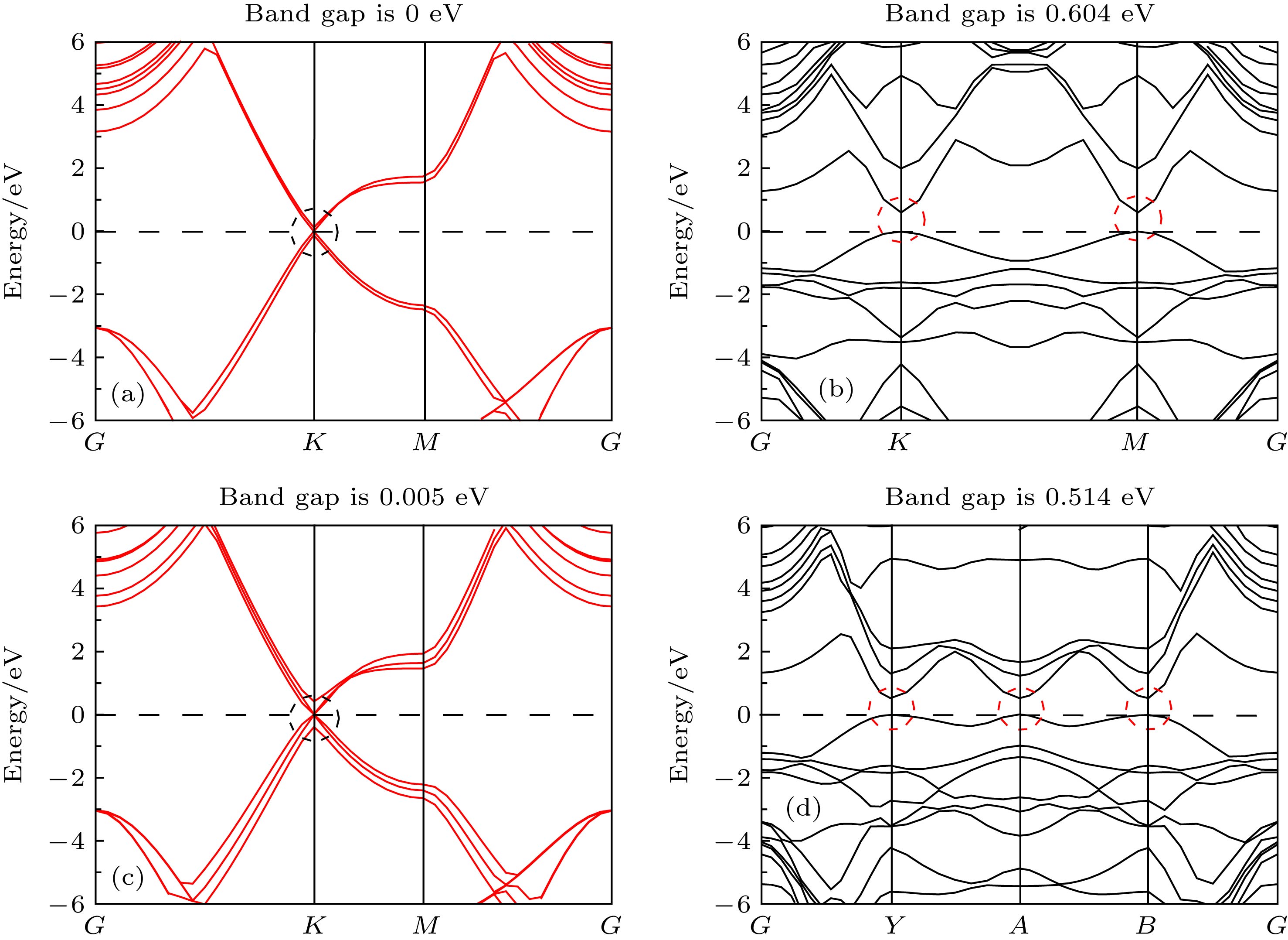 图 2 能带图 (a)双层本征石墨烯; (b)镍掺杂双层石墨烯; (c)三层本征石墨烯; (d)镍掺杂三层石墨烯
 图 3 DOS (a)双层本征石墨烯(D); (b)三层本征石墨烯(T); (c)镍掺杂双层石墨烯(D-Ni); (d)镍掺杂三层石墨烯(T-Ni)


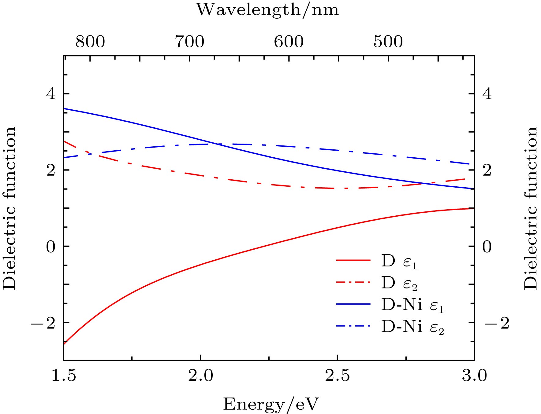 图 4 镍原子掺杂前后的双层石墨烯的介电常数


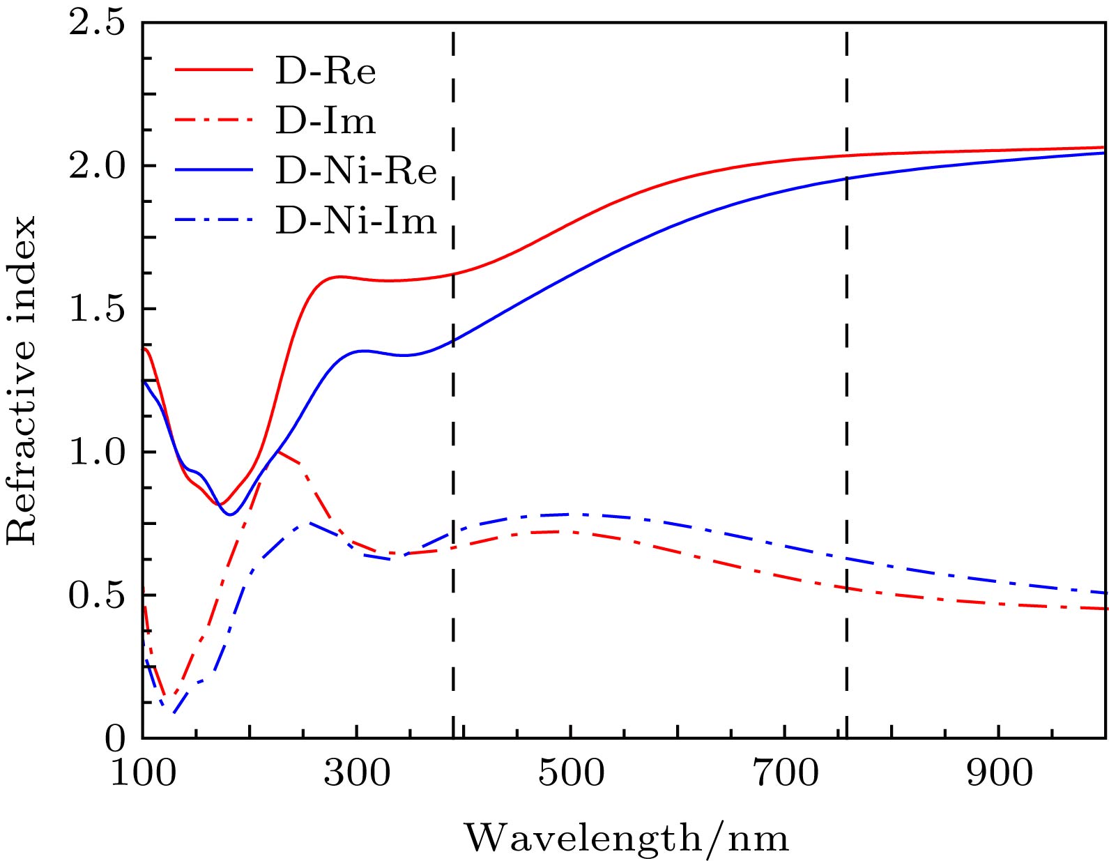 图 5 双层石墨烯掺杂前后的折射率与波长的关系
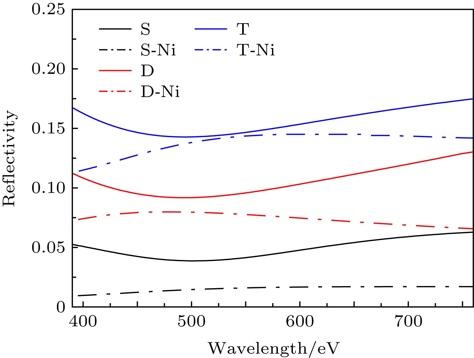 图 6 掺杂前后的单层、双层和三层石墨烯的反射率