PROPAGATION CHARACTERISTICS OF SH GUIDED WAVES IN A PIEZOELECTRIC NANOPLATE 1)
Zhang Lele*, Liu Xianglin??, Liu Jinxi*,2)收稿日期:2018-12-7接受日期:2019-01-18网络出版日期:2019-03-18
| 基金资助: |
Received:2018-12-7Accepted:2019-01-18Online:2019-03-18
作者简介 About authors
2)刘金喜,教授,主要研究方向:压电和磁电弹多场耦合材料与结构的力学行为.E-mail:liujx02@hotmail.com

摘要
压电纳米材料具有机电耦合性强、功耗低和反应灵敏等独特性能,且能满足工程对压电器件微型化的要求,从而在传感、微纳米机电系统和柔性电子器件等领域展现出了广阔的应用前景. 高比表面积引起的表面效应是压电纳米材料最重要的结构特征之一,其对材料的整体力学性质起着决定性的作用.表面效应会导致应力和电位移在压电表面的两侧出现间跃,故传统的力电场连续性条件将不再适用.考虑表面为不计厚度却拥有独立材料参数的薄层,采用表面压电模型计及表面弹性、表面压电性、表面介电性和表面密度的影响,本文研究了压电纳米板中SH型导波的传播特性,给出了板边界处的非典型力电平衡条件,得到了频散方程的解析表达,并结合数值算例详细讨论了表面材料参数和结构尺寸对对称和反对称频散模态的影响.结果表明:SH型导波在压电纳米板中的传播具有明显的尺寸相关性,即当板厚很小时,表面效应会显著改变其频散行为,而随着板厚的增大,表面效应的影响会不断减弱直至可忽略不计.
关键词:
Abstract
Piezoelectric nanomaterials have many unique properties, such as enhanced electromechanical coupling, low power dissipation and sensitive response, etc. Also such materials can meet the demand of microminiaturization of piezoelectric devices. These advantages make them strong candidates for applications in the fields of sensing, nanoelectromechanical systems (NEMS), flexible electronic device, and so on. As one of the most important features of nanomaterials, surface effect which resulted from the high ratio of surface to volume commonly plays a dominant role in the overall mechanical properties of piezoelectric nanomaterials. Due to the presence of surface effect, the bulk stress and bulk electric displacement jump across the piezoelectric surface, thus the classical continuity conditions are invalid. In this paper, the dispersion characteristics of SH guided waves propagating in a monolayer piezoelectric nanoplate are investigated with consideration of the surface effect. A surface is regarded as a two-dimensional continuum of zero thickness which possesses own material properties, and the influences of surface elasticity, surface piezoelectricity, surface permittivity and surface density are accounted into the non-classical boundary conditions of the piezoelectric nanoplate via the surface piezoelectricity model. The analytical expressions of dispersion relations are derived, and the numerical examples are provided to discuss the impacts of surface material parameters and nanoplate thickness on the symmetric and antisymmetric modes. Analysis results show that the propagation characteristics of SH guided waves exhibit obvious size-dependence. The surface effect has a significant impact on dispersion behaviors when the nanoplate thickness is small enough, while they may become more and more negligible as the thickness increases.
Keywords:
PDF (6485KB)元数据多维度评价相关文章导出EndNote|Ris|Bibtex收藏本文
本文引用格式
张乐乐, 刘响林, 刘金喜. 压电纳米板中SH型导波的传播特性 1). 力学学报[J], 2019, 51(2): 503-511 DOI:10.6052/0459-1879-18-413
Zhang Lele, Liu Xianglin, Liu Jinxi.
引 言
在经典连续介质力学中,表面区域被限定为是由少数可忽略的原子层或分子层组成的.然而,当材料尺寸进入纳米量级时,表面与基质的体积比将显著增大,由此引起的表面效应将会对材料的力学性质产生巨大的影响[1-4].因此,近年来纳米材料与结构的表面效应问题一直受到国内外研究者的关 注[5-6].目前,针对各类纳米材料整体力学性能的研究已陆续展开,所采用的方法主要分为三类:实验测量、分子动力学模拟和理论分析[5-9].纳米试验技术难度大且费用高昂,实际有条件开展的课题组少之又少.分子动力学模拟对计算机的运行速度和存储能力要求很高,计算规模的局限性使得该方法能够模拟的尺寸十分有限.理论分析主要是引入一类能反映纳米材料结构特征的内禀系数,通过对现有连续介质模型进行必要的修正来预测材料的力学性能.修正的连续介质模型不仅概念清晰,而且具有较高的计算精度,因而受到了众多****的认可和使用.其中,由Gurtin和Murdoch[10-11]提出的表面弹性理论因物理意义明确且数学表达易用,已成为研究弹性固体表面效应最为行之有效的理论模型.表面弹性理论在纳米力学领域取得了巨大的成功,其准确预测了诸多与经典结果大相径庭的新奇结论[5-6].
随着智能器件逐渐向微型化方向发展,开发各类多功能纳米材料已成为一种趋势.其中,压电纳米材料以其机电转换性强、功耗低和反应灵敏等优异性能受到了人们的广泛关注,已被成功用于制作发电机、传感器、驱动器、谐振器和医用探测器等纳米智能装置[12-15].由于压电纳米材料独特的力电耦合特性,使得表面弹性理论并不适用于研究此类材料的表面效应.为了考虑表面压电和表面介电性能的影响,Yu等[16-17]通过扩展表面弹性理论建立了表面压电模型.目前,表面压电模型已逐步为众多研究者所采纳,成为研究压电材料表面效应的有力工具.基于表面压电模型,Yan和Jiang[18-20]研究了压电纳米梁、板结构的屈曲、振动和机电耦合特性;Chen[21]预测了1-3型纳米压电复合材料的整体有效模量;Wang和Wang[22]分析了圆形压电纳米板在外压作用下的能量收集行为;Zhang等[23]揭示了外加电场作用下,纳米级压电制动器的横向变形对表面参数的依赖性.
弹性导波在压电纳米板结构中的传播原理,是研制和开发各类纳米压电换能器和传感器的理论基础.为此,本文采用表面压电模型研究了SH波在单层压电纳米板中的传播特性,给出计及表面效应的频散方程,并结合数值算例详细讨论了表面材料参数和结构尺寸对频散模态的影响.
1 波动方程的建立和求解
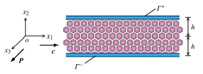
研究对象是一个厚度为$2h$的压电纳米板,其截面如图1所示.当材料进入纳米量级时,表面的影响将不可忽略,为此考虑压电板由上表面$\varGamma ^{ + }$、下表面$\varGamma ^-$和中间的基体三部分组成.在板的中面上建立直角坐标系$ox_{1}x_{2}x_{3}$,定义$\varGamma ^{ + }$和$\varGamma ^-$分别由平面$x_{2}=h$和$x_{2} =-h$确定.假定压电板是横观各向同性的,$x_{1}-x_{2}$平面是各向同性面,$x_{3}$轴正向为极化方向.图1
 新窗口打开|下载原图ZIP|生成PPT
图1压电纳米板及坐标体系的示意图
Fig.1Geometric configuration and coordinate systems of the piezoelectric nanoplate
设定SH波在$x_{1}-x_{2}$平面内传播,则所有场变量均与$x_{3}$无关.在力学上,SH波的传播属于反平面变形问题,仅存在$x_{3}$方向上的位移分量,即
对于横观各向同性压电板,反平面力电耦合问题的控制方程为
式中,$c_{44}$,$e_{15}$和$\kappa _{11}$分别是基体与反平面变形相关的弹性、压电和介电常数,$\rho$是基体的密度,$\phi = \phi \left( {x_1 ,x_2 ,t} \right)$代表压电板在变形下产生的电势.
引入变换$\psi = \phi-\gamma u_3$, 式(2)和式(3)可进一步简化为
式中,$\gamma = e_{15} / \kappa _{11}$,$\bar {c}_{44} = c_{44} + e_{15} \gamma$,$c_{\rm sh} = \sqrt {\bar {c}_{44} / \rho }$是压电介质的体剪切波波速.
考虑SH波沿$x_{1}$轴正向传播,则方程(4)和(5)的解可表示为如下形式
式中,$A_{i}$$(i=1,2,3,4)$为待定的波幅,c是导波的波速,$\omega$是波传播的频率,$k = \omega / c$表示$x_{1}$方向上的波数,$\lambda = \sqrt {\left| {1-\left( {c / c_{\rm sh} } \right)^2} \right|}$定义了波动在$x_{2}$方向上的分布.可以看出,式(6)和式(7)分别代表了两种波速情况下的位移解形式.对于经典的绝缘压电板,SH型导波各阶模态的波速均不会小于体剪切波波速$c_{\rm sh}$,但是当考虑表面效应的影响时,导波低阶模态的波速可能会有小于$c_{\rm sh}$的情形出现,详细的讨论会在数值算例中给出.
很明显,式(6)~式(8)可以分解成关于$x_{1}-x_{3}$平面的对称分量和反对称分量.因此,可考虑如下两个独立的电弹场
式中,上标sy和an分别代表对称模态和反对称模态.
2 频散方程
根据经典的压电本构理论,基体中非零的应力场$\sigma _{3\gamma } (\gamma = 1,2)$和电位移场$D_\gamma$可表示为唯象表面理论通常视表面区域为不计厚度的薄层,且拥有区别于均匀块体的材料特性.从连续介质力学的角度来看,这种将表面二维化的做法在理论分析上具有明显的便利性,即表面效应的影响可概括于对经典边界条件的若干必要修正之中.在表面压电模型中,表面应力和表面电位移的存在会使得体应力和体电位移在表面两侧出现间跃,进而引入了一类"非经典"的应力——电位移边界条件[21,24-25].对于反平面变形而言,这种间跃可写为[21]
式中,$\sigma _{31}^{\rm s}$是表面应力,$D_1^{\rm s}$是表面电位移,$\rho _{\rm s}$是表面密度,$\rho _{\rm s} \ddot {u}_3$代表表面处沿$x_{3}$方向的惯性力.
表面压电模型认为表面和基体之间的连接没有滑移,即位移和电势在表面处是连续的.考虑表面层和基体同样具有横观各向同性,则表面处存在的电弹场可表示为
其中
式中,$\sigma _0$和$D_0$是表面切向的残余应力和残余电位移,$c_{44}^{\rm s}$,$e_{15}^{\rm s}$和$\kappa _{11}^{\rm s}$分别是表面处的弹性、压电和介电系数.
将相应的应力和电位移表达式代入边界条件(17)和(18)中,即可得到一组关于波幅$A_{i}$的线性代数方程组.方程组有非零解的充要条件是其系数行列式为零,由此得到压电纳米板中SH波传播的频散关系.对于对称模态,其频散方程为
同理,对于反对称模态,其频散方程为
基于表面弹性理论,Murdoch[26]曾指出当表面参数满足一定条件时,弹性半空间表面存在SH波,且它是频散的.对于考虑表面效应的压电半无限大固体,本文得到了与Murdoch相似的结论,详细推导见附录.由于高频波对应的波长非常短,故波数$k \to \infty$时有限厚度的压电板就如同是压电半空间.取波数$k \to \infty$,方程(22)和(24)均退化为
上式与附录中给出的压电半空间中SH型表面波的频散方程(A6)是一致的.
当忽略表面效应时,即令所有与表面相关的参数为零,式(17)和式(18)退化为经典的应力自由、电学开路的边界条件.此时方程(22)和(24)不再成立,方程(23)和(25)分别变为
若定义无量纲频率$K = \omega h / c_{\rm sh}$,则方程(27)和(28)的解可表示为
其中,整数$n$定义了SH波的模态阶数.对于对称模态,$n \in \left\{ {0,2,4\cdots } \right\}$为偶数;反之,对于反对称模态,$n \in \left\{ {1,3,5\cdots } \right\}$为奇数.
3 数值算例与分析
在已有的文献中,很多关于压电纳米结构力学行为的研究都是以锆钛酸铅(PZT)为例给出数值结果[18-22,25]. 为此,本文选取PZT-5H进行计算,其具体的材料参数为:$c_{44} = 23$ GPa,$e_{15} = 17$ C/m$^2$,$\kappa _{11} = 1.505\times 10^{-11}$ C/Vm,$\rho = 7500$ kg/m$^{3}$.表面材料特性原则上可通过相关实验和原子模拟的方法确定,但目前文献中能找到的表面参数却寥寥无几.为了定性地揭示表面效应对压电纳米结构力学行为的影响机制,更通用的做法是令表面和基体的材料参数各自由一个纳米量级的特征长度相关联,即设
式中,$f_{\rm c}$,$f_{\rm e}$,$f_{\rm \kappa }$和$f_{\rm \rho }$分别为表征表面弹性、表面压电性、表面介电性和表面密度大小的特征长度.
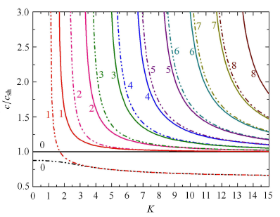
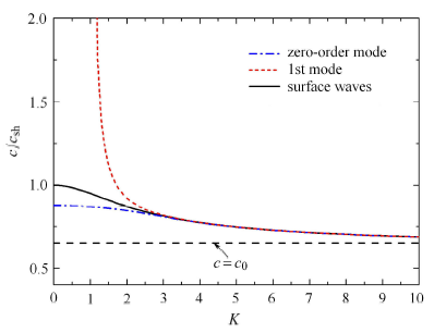
图2给出了经典和纳米压电板中SH型导波的前八阶频散曲线,其中零阶、二阶、四阶、六阶和八阶曲线对应于对称模态,一阶、三阶、五阶和七阶曲线对应于反对称模态. 取$f_{\rm c}=f_{\rm e} =0.5$ nm和$f_{\kappa }=f_{\rho }=1.0$ nm来描述表面效应的影响,经典板的情形由$f_{\rm c}=f_{\rm e}=f_{\kappa }=f_{\rho }=0$ nm来表征.从图中可以看出,考虑表面效应的压电纳米板与经典板相比,其对应模态的频散曲线发生了显著的改变.对于经典板而言,其零阶模态在整个频域上都有$c=c_{\rm sh}$,表明零阶模态不频散,且以恒速度$c_{\rm sh}$传播;而其他阶模态的相速度在截止频率处迅速减小,并随着频率的增大逐渐趋于体剪切波速$c_{\rm sh}$.这说明对于应力自由电学开路的经典压电板而言,SH型导波任意模态的波速都不会低于$c_{\rm sh}$.然而随着表面效应的出现,压电纳米板的前两阶模态(零阶和一阶)均会以小于$c_{\rm sh}$值的波速传播,而且波速会随着k的不断增大而减小,因此都是频散的.众所周知,零阶和一阶模态分别是SH型导波最低阶的对称和反对称模态,当无量纲的频率$K \to \infty$时,它们的传播速度会逼近于半空间中的SH波波速.对于绝缘的经典压电板来说,其对应的半空间不存在表面波,因此零阶和一阶模态的相速度会趋于体剪切波速$c_{\rm sh}$;然而,当表面参数满足条件(A12)时,考虑表面效应的压电半空间中会有SH型表面波的传播,所以此时零阶和一阶模态的相速度会趋于表面波的波速.由于SH型表面波的波速恒小于体剪切波速$c_{\rm sh}$,故这两阶模态会以小于$c_{\rm sh}$的波速传播.图3给出压电纳米板的零阶、一阶模态和相应半空间中SH型表面波的频散曲线.可以看出,由于表面效应而出现的表面波,其速度起始于体剪切波速$c_{\rm sh}$,随着频率的不断增大而逼近于一定值$c_{0}$,其中$c_{0}$是完全由表面参数确定的,这与附录中理论推导的结果是完全一致的(式(A11)).当k增大到某一足够大值后,图3中的三条曲线重合,表明此时压电纳米板中的零阶和一阶模态变为了表面波.
图2
 新窗口打开|下载原图ZIP|生成PPT
图2压电板中SH型导波的前八阶频散曲线 (实线代表经典板,点划线代表取$f_{\rm c}=f_{\rm e} =0.5$ nm,$f_{\kappa }=f_{\rho } =1.0$ nm时的纳米压电板)
Fig.2Dispersion curves of the first eight modes for SH guided waves in a piezoelectric plate (Solid lines indicate the case of the classical piezoelectric plate, and dashed-dotted lines indicate the case of the piezoelectric nanoplate with$f_{\rm c}=f_{\rm e} =0.5$ nm and$f_{\kappa }=f_{\rho } =1.0$ nm)
图3
 新窗口打开|下载原图ZIP|生成PPT
图3压电纳米板中的前两阶模态和相应半空间中SH型表面波的频散曲线
Fig.3Dispersion curves of the lowest two modes for the piezoelectric nanoplate and the SH surface waves for piezoelectric half-space with surface effect
对于图2中的其他高阶模态而言,表面效应的出现会改变其截止频率的发生位置,且模态阶数越高,这种变化越显著.随着频率的不断增大,无论是纳米压电板还是经典板,这些高阶模态的相速度都会迅速衰减至体剪切波速$c_{\rm sh}$.
3.1 表面材料参数对频散特性的影响
压电纳米材料的表面效应是同时包含表面弹性、表面压电性、表面介电性、表面密度以及表面残余场量影响的一种综合效应. Gurtin和Murdoch[27]曾指出,表面残余应力对反平面剪切波的传播没有影响.本文给出的频散方程(22)~(25)同样表明,表面残余应力和残余电位移不会改变SH型导波的传播特性.下面将分别研究四类表面参数单独变化时对频散曲线的影响.不失一般性,以最低阶的对称和反对称模态为例.
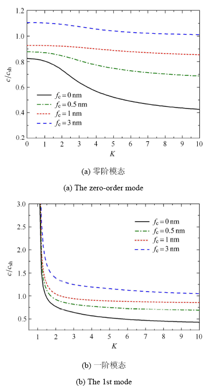
图4给出了不同表面弹性参数下,压电纳米板中SH型导波前两阶模态的频散曲线.对比图中$f_{\rm c} =0$ nm和$f_{\rm c} \ne 0$ nm的情形可知,表面弹性的出现会提高导波的传播速度.随着表面弹性参数的增大,波传播的速度也会逐渐增大.出现这个现象的原因可以解释为:当计入表面弹性的贡献后,压电纳米板的整体刚度会增加,且表面弹性越大,相应地,整体刚度也越大.从图中还可以看出,表面弹性参数的改变对一阶模态的截止频率影响很小,几乎可忽略不计.注意到取$f_{\rm c}=3$ nm时,条件(A12)不再成立,即考虑表面效应的压电半空间中不存在SH型的表面波. 此时,零阶和一阶模态不会以小于$c_{\rm sh}$的波速传播,当频率逐渐增大后,其对应的相速度会缓慢逼近于体剪切波速$c_{\rm sh}$.需要特别说明的是,以下图中表面参数的选取也会不满足条件(A12),其现象与上述情形类似,故后文将不再赘述.
图4
 新窗口打开|下载原图ZIP|生成PPT
图4表面弹性参数对前两阶模态的影响 ($f_{\rm e} =0.5$ nm,$f_{\kappa }=f_{\rho }=1.0$ nm)
Fig.4The lowest two modes with different surface elasticity ($f_{\rm e} =0.5$ nm,$f_{\kappa }=f_{\rho }=1.0$ nm)
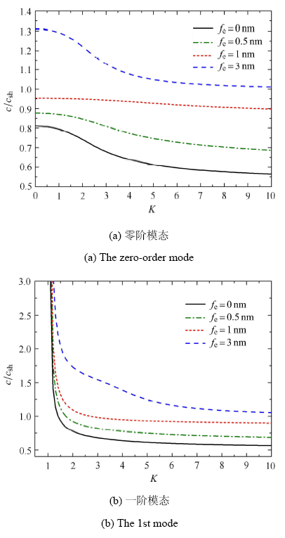
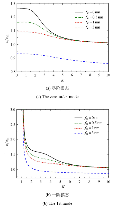
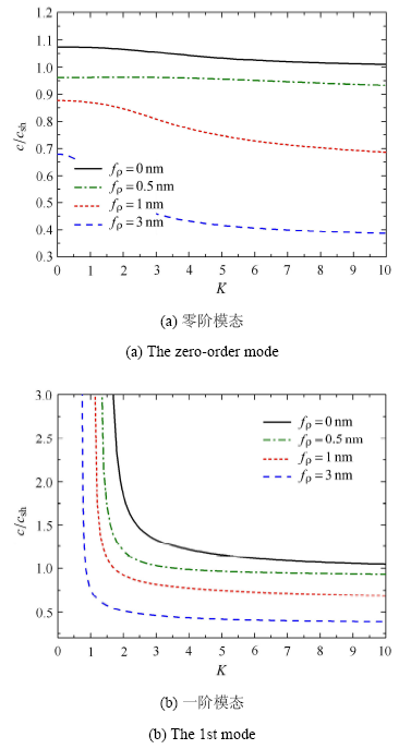
图5~图7分别给出了表面压电性、表面介电性和表面密度对压电纳米板中SH型导波前两阶模态的影响.可以看出,表面压电性显著提高了波的传播速度,而表面介电性和表面密度的存在会使波速明显地降低.当表面压电参数变大时,波传播的速度也随之变大,相反地,随着表面介电性和表面密度的增加,模态的相速度值会不断减小.与表面弹性的影响类似,表面压电性和表面介电性对一阶模态截止频率的改变也是微乎其微的.综合考虑图4~图7可知,表面效应对SH型导波截止频率的影响基本是由表面密度主导的.较大的表面密度会导致较小的截止频率,故表面密度的出现会增大高阶模态可传播的频率范围.
图5
 新窗口打开|下载原图ZIP|生成PPT
图5表面压电参数对前两阶模态的影响 ($f_{\rm c}=0.5$ nm,$f_{\kappa }=f_{\rho } =1.0$ nm)
Fig.5The lowest two modes with different surface piezoelectricity($f_{\rm c}=0.5$ nm,$f_{\kappa }=f_{\rho } =1.0$ nm)
图6
 新窗口打开|下载原图ZIP|生成PPT
图6表面介电参数对前两阶模态的影响 ($f_{\rm c} =0.1$ nm,$f_{\rm e}=2$ nm,$f_{\rho } =1.0$ nm)
Fig.6The lowest two modes with different surface permittivity($f_{\rm c} =0.1$ nm,$f_{\rm e}=2$ nm,$f_{\rho } =1.0$ nm)
图7
 新窗口打开|下载原图ZIP|生成PPT
图7表面密度对前两阶模态的影响 ($f_{\rm c}=f_{\rm e} =0.5$ nm,$f_{\kappa }=1.0$ nm)
Fig.7The lowest two modes with different surface mass density($f_{\rm c}=f_{\rm e} =0.5$ nm,$f_{\kappa }=1.0$ nm)
3.2 结构尺寸对频散特性的影响
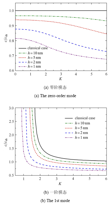
在经典的连续介质力学中,板内SH型导波的传播特性与板厚无关,即不论板厚大小与否,其频散曲线都不会改变.这个现象可在频散方程(29)中得到证实.图8给出了压电纳米板厚度对SH型导波前两阶模态的影响.可以看出,当考虑表面效应的影响时,导波的频散行为具有明显的尺寸相关性,即板厚越小,基于表面压电理论得到的频散图与经典结果的差异越大,这符合表面效应会随着尺寸的减小而增强的物理实际.注意到板厚逐渐增大时,对应于压电纳米板的频散曲线会相应地向经典板情形靠拢.由此可以推断,当板厚增加至某一极限值后,基于表面压电模型得到的频散图将与经典的结果重合,此时表面效应的影响将不复存在.图8
 新窗口打开|下载原图ZIP|生成PPT
图8压电纳米板厚度对前两阶模态的影响($f_{\rm c}=f_{\rm e} =0.5$ nm,$f_{\kappa }=f_{\rho }=1.0$ nm)
Fig.8The lowest two modes with different plate thicknesses($f_{\rm c}=f_{\rm e} =0.5$ nm,$f_{\kappa }=f_{\rho }=1.0$ nm)
4 结 论
基于表面压电模型,本文推导了压电纳米板中SH型导波传播的频散方程,详细讨论了表面材料参数以及结构尺寸对对称和反对称频散模态的影响.研究结果表明:(1) 与经典板的情形不同,压电纳米板中的零阶模态是频散的,且零阶和一阶模态可能会以小于体剪切波速的速度传播;
(2)表面弹性和表面压电性会提高波传播的速度,相反地,表面介电性和表面密度会降低波传播的速度;截止频率会随着表面密度的增加而相应减小,而表面弹性、表面压电性和表面介电性对截止频率的影响很小;
(3)压电纳米板中SH型导波的传播行为表现出了明显的尺寸相关性,当板厚达到一个临界值时,表面效应的影响可忽略不计;
(4)当表面材料参数满足一定条件时,考虑表面效应的压电半空间中存在频散的SH型表面波.
附 录
考虑一横观各向同性的压电半无限大固体占据了空间$\{ {\pmb x}: x_{2} \geqslant 0 \}$,其表面由平面$x_{2} =0$定义.对应于SH型表面波沿$x_{1}$方向传播时的基本解为
条件$\mathop {\lim }\limits_{x_2 \to + \infty } u_3 = 0$要求必须满足$\lambda > 0$,故有
考虑表面效应的影响,则$x_{2} =0$处的边界条件可写为
将式(A1)和式(A2)代入式(15)和式(16)、式(19)和式(20)以及式(A4)和式(A5)中,可以得到一个关于系数A和$B$的线性代数方程组. 令方程组的系数行列式为零,得
显然,压电半空间中受表面效应影响的SH型表面波是频散的,式(A6)即为其相应的频散方程.
由于$\lambda > 0$,所以式(A6)的右端项须满足
其中,$g\left( k \right) = \frac{\bar {e}_{15}^{\rm s} \left( {e_{15}^{\rm s} k + e_{15} } \right)}{\kappa _{11}^{\rm s} k + \kappa _{11} }$是关于k的函数.
对函数$g\left( k \right)$求一阶导数,得
因此,$g\left( k \right)$是关于k的单调递增函数.由此可知
取式(A7)右端函数的最大值,即令
式中,$c_0$为$k \to \infty$时频散方程(A6)的相速度解.
综合考虑式(A3)、式(A7)和式(A10),可知
因此,考虑表面效应的压电半空间中存在SH型表面波的条件为
由于$c_{\rm sh}$和$c_0$分别对应于$k \to$0和$k \to \infty$时的表面波波速,所以方程(A6)确定的频散曲线必定是起始于剪切波速$c_{\rm sh}$而趋近于极限值$c_0$.
当不考虑压电效应时,即令$e_{15} = 0$和$e_{15}^{\rm s} = 0$,式(A12)变为
式中,$c_{\rm sh}^e$表示各向同性弹性介质的剪切波速,且有
式(A13)给出了考虑表面效应的各向同性弹性半空间存在SH型表面波的条件,这与Murdoch的结论是完全一样的[26].
参考文献 原文顺序
文献年度倒序
文中引用次数倒序
被引期刊影响因子
DOIURL

http://link.aip.org/link/APPLAB/v90/i16/p163112/s1&Agg=doi
DOIURL

纳米科技的快速发展使压电纳米结构在纳米机电系统中得到广泛应用,形成了诸如纳米压电电子学等新的研究方向。与传统的宏观压电材料相比,在纳米尺度下压电材料往往呈现出不同的力学特性,而造成这种差异的原因之一便是表面效应。本文基于Stroh公式、Barnett-Lothe积分矩阵及表面阻抗矩阵,研究计入表面效应的任意各向异性压电半空间中的表面波传播问题,导出了频散方程。针对横观各向同性压电材料,假设矢状平面平行于材料各向同性面,发现Rayleigh表面波和B-G波解耦,并得到各自的显式频散方程。结果表明,Rayleigh表面波的波速小于偏振方向垂直于表面的体波,而B-G波的波速小于偏振方向垂直于矢状平面的体波。以PZT-5H材料为例,用数值方法考察表面残余应力和电学边界条件对表面波频散特性的影响发现:表面残余应力只对第一阶Rayleigh波有明显的影响;电学开路情形的B-G波比电学闭路情形的B-G波传播快。本文工作可为纳米表面声波器件的设计或压电纳米结构的无损检测提供理论依据。
DOIURL

纳米科技的快速发展使压电纳米结构在纳米机电系统中得到广泛应用,形成了诸如纳米压电电子学等新的研究方向。与传统的宏观压电材料相比,在纳米尺度下压电材料往往呈现出不同的力学特性,而造成这种差异的原因之一便是表面效应。本文基于Stroh公式、Barnett-Lothe积分矩阵及表面阻抗矩阵,研究计入表面效应的任意各向异性压电半空间中的表面波传播问题,导出了频散方程。针对横观各向同性压电材料,假设矢状平面平行于材料各向同性面,发现Rayleigh表面波和B-G波解耦,并得到各自的显式频散方程。结果表明,Rayleigh表面波的波速小于偏振方向垂直于表面的体波,而B-G波的波速小于偏振方向垂直于矢状平面的体波。以PZT-5H材料为例,用数值方法考察表面残余应力和电学边界条件对表面波频散特性的影响发现:表面残余应力只对第一阶Rayleigh波有明显的影响;电学开路情形的B-G波比电学闭路情形的B-G波传播快。本文工作可为纳米表面声波器件的设计或压电纳米结构的无损检测提供理论依据。
DOIURL

基于表面弹性理论和保角映射技术,研究了远场作用反平面剪切载荷作用下考虑表面弹性效应时正三角形孔边裂纹问题的断裂性能.给出了孔边应力场的精确解,获得了裂纹尖端应力强度因子的解析解答.数值算例中讨论了裂尖应力强度因子随三角形孔尺寸、裂纹长度和表面性能的变化规律.结果表明:当三角形孔的尺寸在纳米量级时,无量纲应力强度因子具有显著的尺寸效应;随着三角形孔尺寸的增大,论文结果趋近于经典断裂理论解答;无量纲应力强度因子随孔边裂纹长度的增加,先增大而后减小;当孔边裂纹长度较小时,表面效应影响较弱;应力强度因子的尺寸效应受表面性能影响显著.
DOIURL

基于表面弹性理论和保角映射技术,研究了远场作用反平面剪切载荷作用下考虑表面弹性效应时正三角形孔边裂纹问题的断裂性能.给出了孔边应力场的精确解,获得了裂纹尖端应力强度因子的解析解答.数值算例中讨论了裂尖应力强度因子随三角形孔尺寸、裂纹长度和表面性能的变化规律.结果表明:当三角形孔的尺寸在纳米量级时,无量纲应力强度因子具有显著的尺寸效应;随着三角形孔尺寸的增大,论文结果趋近于经典断裂理论解答;无量纲应力强度因子随孔边裂纹长度的增加,先增大而后减小;当孔边裂纹长度较小时,表面效应影响较弱;应力强度因子的尺寸效应受表面性能影响显著.
DOIURL

This review article summarizes the advances in the surface stress effect in mechanics of nanostructured elements, including nanoparticles, nanowires, nanobeams, and nanofilms, and heterogeneous materials containing nanoscale inhomogeneities. It begins with the fundamental formulations of surface mechanics of solids, including the definition of surface stress as a surface excess quantity, the surface constitutive relations, and the surface equilibrium equations. Then, it depicts some theoretical and experimental studies of the mechanical properties of nanostructured elements, as well as the static and dynamic behaviour of cantilever sensors caused by the surface stress which is influenced by adsorption. Afterwards, the article gives a summary of the analytical elasto-static and dynamic solutions of a single as well as multiple inhomogeneities embedded in a matrix with the interface stress prevailing. The effect of surface elasticity on the diffraction of elastic waves is elucidated. Due to the difficulties in the analytical solution of inhomogeneities of complex shapes and configurations, finite element approaches have been developed for heterogeneous materials with the surface stress. Surface stress and surface energy are inherently related to crack propagation and the stress field in the vicinity of crack tips. The solutions of crack problems taking into account surface stress effects are also included. Predicting the effective elastic and plastic responses of heterogeneous materials while taking into account surface and interface stresses has received much attention. The advances in this topic are inevitably delineated. Mechanics of rough surfaces appears to deserve special attention due to its theoretical and practical implications. Some most recent work is reviewed. Finally, some challenges are pointed out. They include the characterization of surfaces and interfaces of real nanomaterials, experimental measurements and verification of mechanical parameters of complex surfaces, and the effects of the physical and chemical processes on the surface properties, etc.
DOIURL

We have shown in a series of recent papers that the classical theory of elasticity can be extended to the nanoscale by supplementing the equations of elasticity for the bulk material with the generalized Young-Laplace equations of surface elasticity. This review article shows how this has been done in order to capture the often unusual mechanical and physical properties of nanostructured particulate and porous materials. It begins with a description of the generalized Young-Laplace equations. It then generalizes the classical Eshelby formalism for nano-inhomogeneities; the Eshelby tensor now depends on the size of the inhomogeneity and the location of the material point in it. Then the stress concentration factor of a spherical nanovoid is calculated, as well as the strain fields in quantum dots (QDs) with multi-shell structures and in alloyed QDs induced by the mismatch in the lattice constants of the atomic species. This is followed by a generalization of the micromechanical framework for determining the effective elastic properties and effective coefficients of thermal expansion of heterogeneous solids containing nano-inhomogeneities. It is shown, for example, that the elastic constants of nanochannel-array materials with a large surface area can be made to exceed those of the nonporous matrices through pore surface modification or coating. Finally, the scaling laws governing the properties of nanostructured materials are derived. The underlying cause of the size dependence of these properties at the nanoscale is the competition between surface and bulk energies. These laws provide a yardstick for checking the accuracy of experimentally measured or numerically computed properties of nanostructured materials over a broad size range and can thus help replace repeated and exhaustive testing by one or a few tests.
DOIURL

The effect of reduced size on the mechanical and elastic properties measured on $35\phantom{\rule{0.3em}{0ex}}\mathrm{nm}$ diameter Ni and Co nanowires is presented and discussed. The stresses induced in the nanowires due to the different thermal expansion constants of the metal and alumina change the magnetic properties of the nanowires, allowing one to measure the effective Young's modulus and the surface tension of the nanowires by means of simple magnetometry. The Young's modulus of the longer nanowire is higher than that of the shorter one that is comparable to its bulk value. This effect is successfully attributed to surface tension effects.
DOIURL

界面能密度是表征纳米复合材料与结构界面力学性质的重要物理量.采用分子动力学方法计算了不同面心立方金属晶体构成的双材料纳米薄板结构的界面能密度,分析了界面晶格结构形貌变化及界面效应对原子势能的影响.结果表明:双材料纳米薄板界面具有周期性褶皱状疏密相间的晶格结构形貌,界面上原子势能亦呈现周期性分布特性,而靠近界面的两侧原子势能与板内原子势能具有明显差异.拉格朗日界面能密度和欧拉界面能密度均随双层薄板厚度的增加而增加,最终趋向于块体双材料结构的界面能密度.
DOIURL

界面能密度是表征纳米复合材料与结构界面力学性质的重要物理量.采用分子动力学方法计算了不同面心立方金属晶体构成的双材料纳米薄板结构的界面能密度,分析了界面晶格结构形貌变化及界面效应对原子势能的影响.结果表明:双材料纳米薄板界面具有周期性褶皱状疏密相间的晶格结构形貌,界面上原子势能亦呈现周期性分布特性,而靠近界面的两侧原子势能与板内原子势能具有明显差异.拉格朗日界面能密度和欧拉界面能密度均随双层薄板厚度的增加而增加,最终趋向于块体双材料结构的界面能密度.
DOIURL

基于Euler-Bernoulli梁理论和单向耦合的热传导理论,研究了功能梯度材料(functionally graded material,FGM)微梁的热弹性阻尼(thermoelastic damping,TED).假设矩形截面微梁的材料性质沿厚度方向按幂函数连续变化,忽略了温度梯度在轴向的变化,建立了单向耦合的变系数一维热传导方程.热力耦合的横向自由振动微分方程由经典梁理论获得.采用分层均匀化方法将变系数的热传导方程简化为一系列在各分层内定义的常系数微分方程,利用上下表面的绝热边界条件和界面处的连续性条件获得了微梁温度场的分层解析解.将温度场代入微梁的运动方程,获得了包含热弹性阻尼的复频率,进而求得了代表热弹性阻尼的逆品质因子.在给定金属-陶瓷功能梯度材料后,通过数值计算结果定量分析了材料梯度指数、频率阶数、几何尺寸以及边界条件对TED的影响.结果表明:(1)若梁长固定不变,梁厚度小于某个数值时,改变陶瓷材料体积分数可以使得TED取得最小值;(2)固有频率阶数对TED的最大值没有影响,但是频率阶数越高对应的临界厚度越小;(3)不同的边界条件对应的TED的最大值相同,但是随着支座约束刚度增大对应的临界厚度减小;(4)TED的最大值和对应的临界厚度随着金属组分的增大而增大.
DOIURL

基于Euler-Bernoulli梁理论和单向耦合的热传导理论,研究了功能梯度材料(functionally graded material,FGM)微梁的热弹性阻尼(thermoelastic damping,TED).假设矩形截面微梁的材料性质沿厚度方向按幂函数连续变化,忽略了温度梯度在轴向的变化,建立了单向耦合的变系数一维热传导方程.热力耦合的横向自由振动微分方程由经典梁理论获得.采用分层均匀化方法将变系数的热传导方程简化为一系列在各分层内定义的常系数微分方程,利用上下表面的绝热边界条件和界面处的连续性条件获得了微梁温度场的分层解析解.将温度场代入微梁的运动方程,获得了包含热弹性阻尼的复频率,进而求得了代表热弹性阻尼的逆品质因子.在给定金属-陶瓷功能梯度材料后,通过数值计算结果定量分析了材料梯度指数、频率阶数、几何尺寸以及边界条件对TED的影响.结果表明:(1)若梁长固定不变,梁厚度小于某个数值时,改变陶瓷材料体积分数可以使得TED取得最小值;(2)固有频率阶数对TED的最大值没有影响,但是频率阶数越高对应的临界厚度越小;(3)不同的边界条件对应的TED的最大值相同,但是随着支座约束刚度增大对应的临界厚度减小;(4)TED的最大值和对应的临界厚度随着金属组分的增大而增大.
DOIURL

A mathematical framework is developed to study the mechanical behavior of material surfaces. The tensorial nature of surface stress is established using the force and moment balance laws. Bodies whose boundaries are material surfaces are discussed and the relation between surface and body stress examined. Elastic surfaces are defined and a linear theory with non-vanishing residual stress derived. The free-surface problem is posed within the linear theory and uniqueness of solution demonstrated. Predictions of the linear theory are noted and compared with the corresponding classical results. A note on frame-indifference and symmetry for material surfaces is appended.
DOIURLPMID

We have converted nanoscale mechanical energy into electrical energy by means of piezoelectric zinc oxide nanowire (NW) arrays. The aligned NWs are deflected with a conductive atomic force microscope tip in contact mode. The coupling of piezoelectric and semiconducting properties in zinc oxide creates a strain field and charge separation across the NW as a result of its bending. The rectifying characteristic of the Schottky barrier formed between the metal tip and the NW leads to electrical current generation. The efficiency of the NW-based piezoelectric power generator is estimated to be 17 to 30%. This approach has the potential of converting mechanical, vibrational, and/or hydraulic energy into electricity for powering nanodevices.
DOIURL

By coating one side of the surface of a ZnO nanobelt (NB) with multilayer polymers using an electrostatic self-assembling process, a humidity/chemical nanosensor based on piezoelectric field effect transistor (PE-FET) is demonstrated. The working principle of the PE-FET relies on the self-contraction/expansion of the polymer, which builds up a strain in the piezoelectric NB and induces a potential drop across the NB that serves as the gate voltage for controlling the current flowing through the NB. The response of PE-FET to the phase transition of the coating polymer was also demonstrated. The device is a component for nanopiezotronics.
DOIURLPMID

Piezoelectric nano-structures have been regarded as the next-generation piezoelectric material due to their inherent nano-sized piezoelectricity. This review summarizes the recent theoretical and experimental findings in piezoelectric nano-structures, including piezoelectric nanowires, nanoplates, nanobeams, nanofilms, nanoparticles, and piezoelectric heterogeneous materials containing piezoelectric nano-inhomogeneities. To begin, the types of piezoelectric nano-structured materials and the wide application of piezoelectric nano-structures in recent years are delineated. Next, the theoretical foundations including the definition of surface stress and electric displacement, the surface constitutive relations, the surface equilibrium equations, and nonlocal piezoelectricity, and their applications, are illustrated. Then, the effective mechanical and piezoelectric properties are depicted. Furthermore, the experimental investigations are classified, and some important observations are discussed. Finally, the perspectives and challenges for the future development of piezoelectric nano-structures are pointed out.
DOIURL

A relation on electric field dependent surface stress, or alternatively surface piezoelectricity, is proposed in this paper. Based on such relation, a piezoelectric ring under prescribed potential has been studied and the results show that the surface piezoelectricity may play an important role in the electromechanical behavior of piezoelectric nanostructures. (0008 2006 WILEY-VCH Verlag GmbH & Co. KGaA, Weinheim)
DOIURL

In this paper,a phenomenological continuum theory of surface piezoelectricity accounting for the linear superficial interplay between electricity and elasticity is formulated primarily for elastic dielectric materials.This theory is inspired by the physical idea that once completely relaxed,an insulating free dielectric surface will sustain a nontrivial spontaneous surface polarization in the normal direction together with a tangential self-equilibrated residual surface stress field.Under external loadings,the surface Helmholtz free energy density is identified as the characteristic function of such surfaces,with the in-plane strain tensor of surface and the surface free charge density as the independent state variables.New boundary conditions governing the surface piezoelectricity are derived through the variational method.The resulting concepts of charge-dependent surface stress and deformationdependent surface electric field reflect the linear electromechanical coupling behavior of nanodielectric surfaces.As an illustrative example,an infinite radially polarizable piezoelectric nanotube with both inner and outer surfaces grounded is investigated.The novel phenomenon of possible surface-induced polarity inversion is predicted for thin enough nanotubes.
DOIURLPMID

In this work, the influence of surface effects, including residual surface stress, surface elasticity and surface piezoelectricity, on the vibrational and buckling behaviors of piezoelectric nanobeams is investigated by using the Euler-Bernoulli beam theory. The surface effects are incorporated by applying the surface piezoelectricity model and the generalized Young-Laplace equations. The results demonstrate that surface effects play a significant role in predicting these behaviors. It is found that the influence of the residual surface stress and the surface piezoelectricity on the resonant frequencies and the critical electric potential for buckling is more prominent than the surface elasticity. The nanobeam boundary conditions are also found to influence the surface effects on these parameters. This study also shows that the resonant frequencies can be tuned by adjusting the applied electrical load. The present study is envisaged to provide useful insights for the design and applications of piezoelectric-beam-based nanodevices.
DOIURL

In this letter, surface effects on the vibration and buckling of a clamped-clamped piezoelectric nanoplate (PNP) are investigated by using Kirchhoff plate theory with the incorporation of the surface piezoelectricity model and the generalized Young-Laplace equations. Ritz solutions show that the surface effects on the resonant frequency are more prominent for the PNPs with smaller thickness and larger aspect ratio, with dominant effect from surface piezoelectricity and residual surface stress. Results also suggest potential for frequency tuning of the PNPs via applied electric potentials. Simulation results on the critical buckling potential indicate that the influence of the combined surface effects is the competition between the residual surface stress and surface piezoelectricity. This work is helpful for the characterization of the mechanical properties and design of PNP-based devices.
DOI

This work aims to investigate the electroelastic responses of a thin piezoelectric plate under mechanical and electrical loads with the consideration of surface effects. Surface effects, including surface elasticity, residual surface stress and surface piezoelectricity, are incorporated into the conventional Kirchhoff plate theory for a piezoelectric plate via the surface piezoelectricity model and the generalized Young-Laplace equations. Different from the results predicted by the conventional plate theory ignoring the surface effects, the proposed model predicts size-dependent behaviours of the piezoelectric thin plate with nanoscale thickness. It is found that surface effects have significant influence on the electroelastic responses of the piezoelectric nanoplate. This work is expected to provide more accurate predictions on characterizing nanofilm or nanoribbon based piezoelectric devices in nanoelectromechanical systems. (paper)
DOIURL [本文引用: 2]

We consider the macroscopic behavior of two-phase fibrous piezoelectric composites. The fibers are of circular cross-section with the same radius. Along the interfaces between the fibers and the matrix we consider the effects of surface stress and surface electric displacement. The constituents are transversely isotropic and exhibit pyroelectricity. We find that the overall thermoelectroelastic moduli of these solids must comply with two sets of exact connections. The first set, similar to Hill’s universal connections, provides five constraints between the six axisymmetric overall electroelastic moduli. The second set relates the effective coefficients of thermal stress and pyroelectric coefficients to the effective electroelastic moduli, in analogy with Levin’s formula. In contrast to their conventional counterparts, i.e., without surface effects, the presence of surface effects makes both sets of connections dependent on the absolute size of the nanoinclusions.
DOIURL [本文引用: 1]

The influence of surface effects on the energy-generating performance of piezoelectric circular nanomembrane energy harvesters under blood pressure is studied. The effects of surface elasticity, surface piezoelectricity, residual surface stress and geometry nonlinear strain are incorporated in the present model. An approximated closed-form solution for the electrical energy of the nanomembrane is derived by using the energy method. Results show that positive surface elasticity and residual surface stress reduce the electrical energy and the surface piezoelectricity effect increases the electrical energy. The influence of surface effect on the energy-generating performance of piezoelectric circular membranes is more significant for a membrane with a small thickness and a large radius-to-thickness ratio.
DOIURL [本文引用: 1]

Abstract Two-dimensional (2D) equations of piezoelectric bimorph nano-actuators are presented which take account of the surface effect. The surface effect of the bimorph structure is treated as a surface layer with zero thickness. The influence on the plate's overall properties resulted from the surface elasticity and piezoelectricity is modeled by a spring force exerting on the boundary of the bulk core. Using the derived 2D equations, the anti-parallel piezoelectric bimorph nano-actuators of both cantilever and simply supported plate type are investigated theoretically. Numerical results show that the effective properties and the deflections of the antiparallel bimorph nano-actuators are size-dependent. The deflection at the resonant frequency achieves nearly 50 times as that under the static driving voltage.
DOIURL

In nanoscaled solids, the mathematical behavior of a curved interface between two different phases with interface stress effects can be described by the generalized Young-Laplace equations [T. Young,Philos. Trans. R. Soc. London95,65(1805);P. S. Laplace,Traite de Mechanique Celeste(Gauthier-Villars,Paris,1805), Vol.4, Supplements au Livre X]. Here we present a geometric illustration to prove the equations. By considering a small element of the curved thin interface, we model the interface stresses as in-plane stresses acting along its edges, while on the top and bottom faces of the interface the tractions are contributed from its three-dimensional bulk neighborhood. With this schematic illustration, simple force balance considerations will give the Young-Laplace equations across the interface. Similar procedures can be applied to conduction phenomena. This will allow us to reconstruct one type of imperfect interfaces, referred to as highly conducting interfaces.
DOIURL

61Surface piezoelectricity model is first introduced to investigate the dispersive properties of elastic waves propagating in piezoelectric nanoplates.61The dispersive modes predicted by the theory of surface piezoelectricity exhibit obvious size-dependent behaviors.61In the presence of surface effects, the magnitude of propagating velocity decrease considerably for a given frequency.61The critical plate thickness was predicted, above which the surface effects may vanish.
DOIURL [本文引用: 2]

A study is made of the propagation of Love and Rayleigh waves in elastic bodies whose boundaries support surface stresses, such as crystals cleaved in vacuo or bodies upon which are deposited extremely thin films. The surfaces of such bodies are herein modelled as two-dimensional elastic continua that adhere without slipping to their substrates and in which is located residual stress. The corresponding boundary condition gives rise to behaviour which is contrasted with that occurring in the absence of surface stress. The results are also related to previous studies of surface waves in thin strata superposed on elastic half-spaces, from which the present theory differs by taking into account residual stress. The behaviour is shown to be sensitive to the relative values of the residual stress, elastic moduli, and density of the surface. Attention is drawn to the relevance of the study to those signal-processing devices which utilize surface waves in thin films.
DOIURL [本文引用: 1]

In this paper we consider an elastic half‐space whose free surface is an elastic surface capable of supporting its own stress field. This surface stress is a function of surface strain and is related to the stress in the interior of the body by a nonclassical boundary condition. We here study, within the framework of the appropriate linearized theory, the reflection of plane harmonic waves by the free surface. We show that at very high frequencies the presence of surface stress results in a marked departure from the classical theory.
