全文HTML
--> --> -->中国科学院上海硅酸盐研究所罗豪甦课题组于1996年成功生长出了以铌镁酸铅钛酸铅Pb(Mg1/3Nb2/3)O3-PbTiO3 (PMN-PT或PMNT)弛豫铁电单晶为代表的新一代高性能大尺寸压电材料, 尺寸达到了Φ75 mm×60 mm, 而其压电性能d33 和居里温度Tc分别达到2000 pC/N和155 ℃, 长度振动伸缩模式k33高达92%, 这类弛豫型铁电单晶已经成为新一代超声换能器、传感器以及驱动器的核心压电材料[5-9]. 三元体系铌铟酸铅铌镁酸铅钛酸铅x Pb(In1/2Nb1/2)O3-yPb(Mg1/3Nb2/3)O3-(1 – x – y) PbTiO3 弛豫型铁电单晶(简称PIN-PMN-PT或PIMNT[10-15] 单晶)引起了铁电研究领域的广泛关注, PIMNT单晶通过In元素的添加, 居里温度和三方-四方相变温度以及矫顽场都得到了一定程度的提高, 拓宽了弛豫铁电单晶的应用温度范围, 可以有效避免单晶在使用过程中因温度过高引起退极化的现象. 因此, 三元体系的PIMNT单晶是一种更具有应用前景的新型压电材料. 与此同时, 研究人员发现Mn离子掺杂可以显著提高PIMNT单晶的居里温度, Mn-PIMNT单晶的压电性能d33和居里温度Tc分别达到836 pC/N和187 ℃[16-19].
西安交通大学Zhang等[20]通过紫外光刻-深反应离子刻蚀工艺刻蚀PMN-PT单晶得到了深度约为30 μm、缝宽为10 μm的压电单晶阵列, 其侧壁角度达到84°. 北卡罗来纳州立大学Jiang等[21]同样通过紫外光刻-深反应离子刻蚀工艺刻蚀PMN-PT单晶得到了刻蚀深度约为60 μm、缝宽约为5 μm的压电单晶阵列, 侧壁角度达83.5°, 制备得到的复合材料的频率为49.05 MHz, 机电耦合系数为66%. 该方法制备得到的复合材料具有高频率、高机电耦合性能的特征.
采用高居里温度Mn掺杂0.3Pb(In1/2Nb1/2)O3-0.4Pb(Mg1/3Nb2/3)O3-0.3PbTiO3 (Mn-PIMNT)单晶, 通过引入半导体工艺中的磁控溅射、紫外光刻、电镀及深反应离子刻蚀方法制备高密度面阵. 该方法可以制备出更低缝宽(低于5 μm)、高机电耦合性能的高密度复合材料. 同时, 本文还研究了刻蚀后微米尺度下的铁电畴结构及其电场性能的调控规律. 此项工作能够有效地促进高密度、高频率、高机电耦合性能面阵换能器[22-26]的发展.
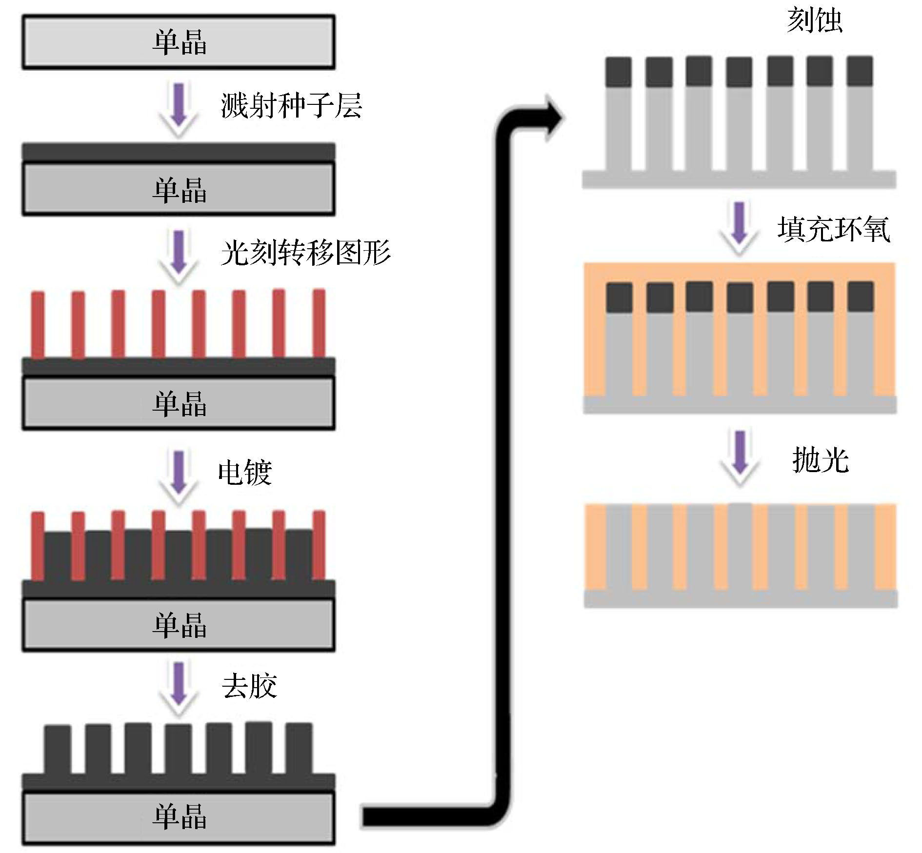 图 1 实验流程图
Figure1. Flow chart of the whole experiment.
将刻蚀后的压电单晶阵列进行环氧树脂(Epoxy)填充后烘干, 经过精密研磨抛光机抛光表面后, 用压电力显微镜(MFP-3D)对微米尺度压电单晶复合材料的铁电畴结构进行表征.
3.1.磁控溅射镍种子层
将整体平行度小于1 μm、尺寸为10 mm × 10 mm的正方形Mn-PIMNT单晶抛光后, 在其表面通过磁控溅射设备(ULVAC)生长一层厚度约为200 nm的镍种子层, 生长条件为直流电源功率为60 W、气体氛围为Ar、衬底转速为6 r/min、时间为15 min, 其作用是为后续的电镀过程提供导电接触面, 保证电镀掩模从显影后的凹槽中生长出来.2
3.2.紫外光刻
紫外光刻的原理是紫外光透过掩模版照射到光刻正胶表面, 从而使透光区域的光刻正胶能够被显影液溶解, 不透光区域的光刻正胶则得以保留. 紫外光刻实验之后, 用扫描电子显微镜(TESCAN VEGA 3及S-4800)测量紫外光刻后样品的截面, 得到深度约10 μm的光刻图案, 如图2所示. 图 2 紫外光刻实验结果 (a), (b) 阵元尺寸为12.94 μm时, 光学显微镜下的表面形貌和扫描电子显微镜下的截面图; (c), (d) 阵元尺寸为13.97 μm时, 光学显微镜下的表面形貌和扫描电子显微镜下的截面图
Figure2. Results of lithography: (a), (b) Surface morphology under optical microscope and cross section under scanning electron microscope when the element size is 12.94 μm; (c), (d) surface morphology under optical microscope and cross section under scanning electron microscope when the element size is 13.97 μm.
图2(a)与图2(c)分别为图2(b)与图2(d)在光学显微镜下所对应的表面形貌, 图2(b)与图2(d)中得到深度分别为10.00 μm与9.92 μm的光刻图案, 图案的垂直度达到89°. 光刻图案的结构示意图如图3所示, 图案垂直度由如下公式得到:
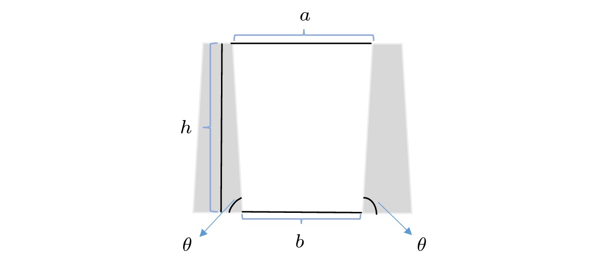 图 3 光刻图案结构示意图
Figure3. Schematic diagram of lithographic pattern structure.
2
3.3.电 镀
电镀原理是用外加电流还原溶解在氨基磺酸镍电镀液中的镍阳离子, 从而在光刻后裸露的镍种子层表面得到高度为10 μm的镍金属掩模. 该掩模的作用是增加刻蚀选择比, 依赖于金属镍与单晶不同的刻蚀速率最终得到高密度阵列. 电镀液成分及含量如表1所列. 电镀后的表面与截面在扫描电子显微镜下分别如图4(a)与图4(b)所示.| 成分 | 含量 |
| 氨基磺酸镍/g·L–1 | 280—400 |
| 硼酸/g·L–1 | 40—50 |
| 阳极活化剂/g·L–1 | 60—100 |
| 润湿剂/mL·L–1 | 1—5 |
| 去应力剂 | 适量 |
表1电镀液配料成分及含量
Table1.Composition and content of electroplate bath ingredients.
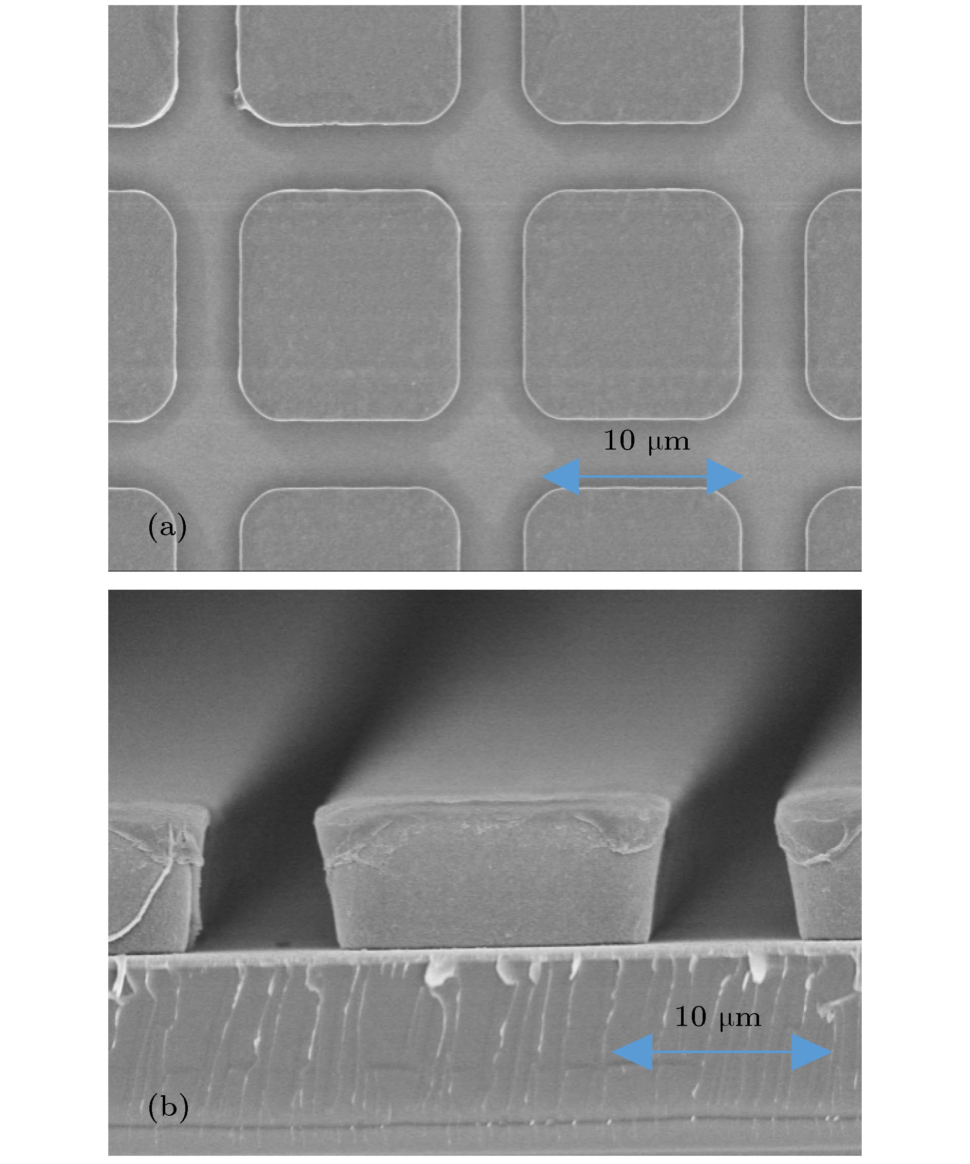 图 4 电镀实验结果 (a) 扫描电子显微镜下的表面; (b) 扫描电子显微镜下的截面
Figure4. Electroplating experiment results: (a) Surface under scanning electron microscope; (b) cross section under scanning electron microscope.
电镀反应方程式为
阳极: Ni – 2 e–→ Ni2+; 阴极: Ni2++2 e–→Ni.
2
3.4.深反应离子刻蚀
深反应离子刻蚀是通过外部施加的射频电场沿磁中性环路产生等离子体, 等离子体的能量与被刻蚀层发生反应, 依赖于金属镍与单晶不同的刻蚀速率从而得到高密度阵列. 其中, 刻蚀深度通过扫描电子显微镜测量得到.改变刻蚀参数, 得到刻蚀速率与天线功率(图5(a))、偏置功率(图5(b))以及气体流量比(图5(c))的变化关系. 其中, 气体流量比 = [SF6气体流量/(SF6气体流量 + Ar气体流量)] × 100%.
 图 5 刻蚀速率实验结果 (a) 刻蚀速率与天线功率的关系; (b) 刻蚀速率与偏置功率的关系; (c) 刻蚀速率与刻蚀气体流量比的关系
Figure5. Etching rate experimental results: (a) Relationship between etching rate and antenna power; (b) relationship between etching rate and bias power; (c) relationship between etching rate and etching gas flow ratio.
由图5(a)可知, 随着天线功率的增大, Mn-PIMNT单晶的刻蚀速率有增大的趋势, 但并不是天线功率越大刻蚀速率越快, 当天线功率增大到800 W时, 刻蚀速率达到最大值, 为5.5 nm/s, 继续增大天线功率, 刻蚀速率会减小. 当偏置功率从100 W增大到400 W时, 刻蚀速率从2.2 nm/s增大至5.4 nm/s, 当偏置功率继续从400 W增大至600 W时, 刻蚀速率从5.4 nm/s降低至4.95 nm/s, 如图5(b)所示. 当气体流量比从10%增大至40%时, 刻蚀速率几乎是线性增大的, 从4.2 nm/s增大至6.7 nm/s, 但是继续把气体流量比从40%增大至50%时, 刻蚀速率会降低, 如图5(c)所示.
因此, 当天线功率为800 W, 偏置功率为400 W, 气体流量比为40%时, 刻蚀速率达到最快, 其刻蚀的沟槽宽度及深度也是在掩模板的尺寸所允许的范围内. 以此最佳条件, 调整了不同的刻蚀时间分别得到如图6(b)—(d)的阵列, 其中图6(a)与图6(b)为高密度方形阵列, 阵元尺寸达11.9 μm, 刻蚀深度大于5 μm, 沟槽宽度小于5 μm, 侧壁角度可控、最高达87°. 图6(c)为刻蚀出的锥形阵列, 刻蚀深度为21.9 μm. 图6(d)为刻蚀得到的深度约为30 μm的方形阵列, 阵元尺寸达11.3 μm, 沟槽宽度低于5 μm, 侧壁角度大于87°.
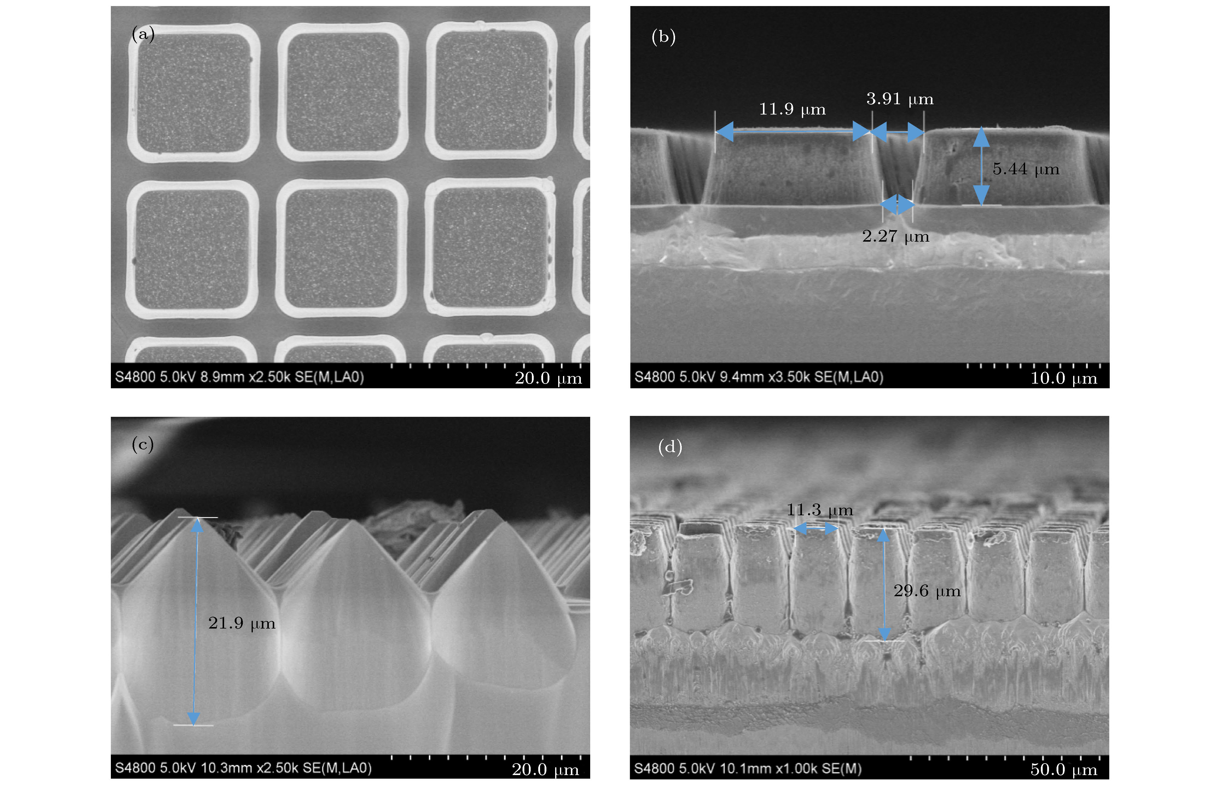 图 6 刻蚀结果 (a) 高密度面阵表面形貌; (b) 高密度面阵截面形貌; (c) 锥形阵列截面形貌; (d) 深刻蚀高密度面阵截面形貌
Figure6. Etching results: (a) Surface morphology of high density array; (b) cross section morphology of high density array; (c) cross section morphology of conical array; (d) the surface morphology of deep etching of high density surface array.
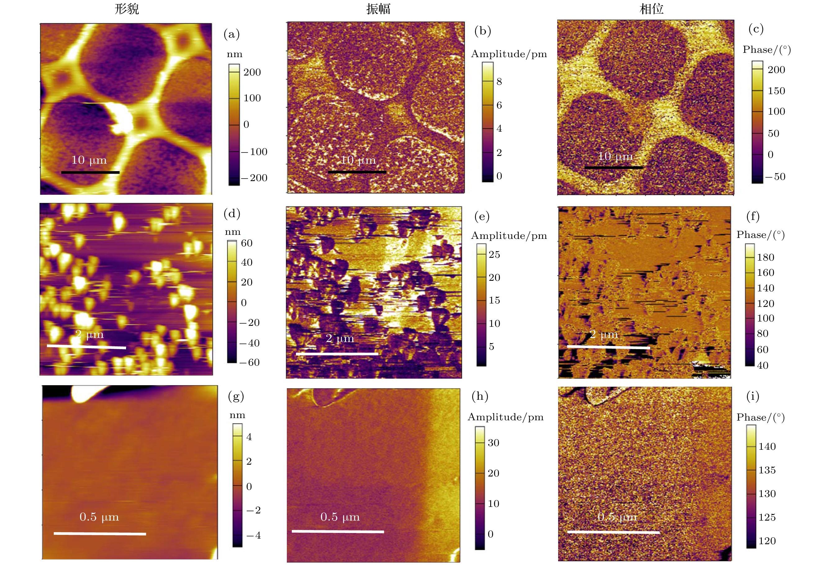 图 7 压电力显微镜下的不同尺度区域结构 (a) 30 μm × 30 μm区域的表面形貌; (b) 30 μm × 30 μm区域的面外振幅; (c) 30 μm × 30 μm区域的相位; (d) 5 μm × 5 μm区域的表面形貌; (e) 5 μm × 5 μm区域的面外振幅; (f) 5 μm × 5 μm区域的相位; (g) 1 μm × 1 μm区域的表面形貌; (h) 1 μm × 1 μm区域的面外振幅; (i) 1 μm × 1 μm区域的相位
Figure7. Structure of different scale areas under the piezoelectric microscope: (a) Surface morphology of 30 μm × 30 μm area; (b) out of plane amplitude of 30 μm × 30 μm area; (c) phase of 30 μm × 30 μm area; (d) surface morphology of 5 μm × 5 μm area; (e) out of plane amplitude of 5 μm × 5 μm area; (f) phase of 5 μm × 5 μm area; (g) surface morphology of 1 μm × 1 μm area; (h) out of plane amplitude of 1 μm × 1 μm area; (i) phase of 1 μm × 1 μm area.
在1 μm × 1 μm的区域中分别施加±10 V (图8(a)与图8(b)), ±20 V (图8(c)与图8(d))和±30 V (图8(e)与图8(f))的“回”字形电压, 明显观察到了Mn-PIMNT单晶复合材料的铁电畴结构在不同电压下的演变过程. 同时, 还发现图8(c)—图8(f)的“回”字形电压偏离中心位置, 而图8(a)与图8(b)的“回”字形电压处于中心位置. 由于压电力显微镜探针扫描区域较小, 如果对压电力显微镜探针施加的直流电压增大, 会使探针振动幅度变大, 造成了“回”字形电压偏离中心位置.
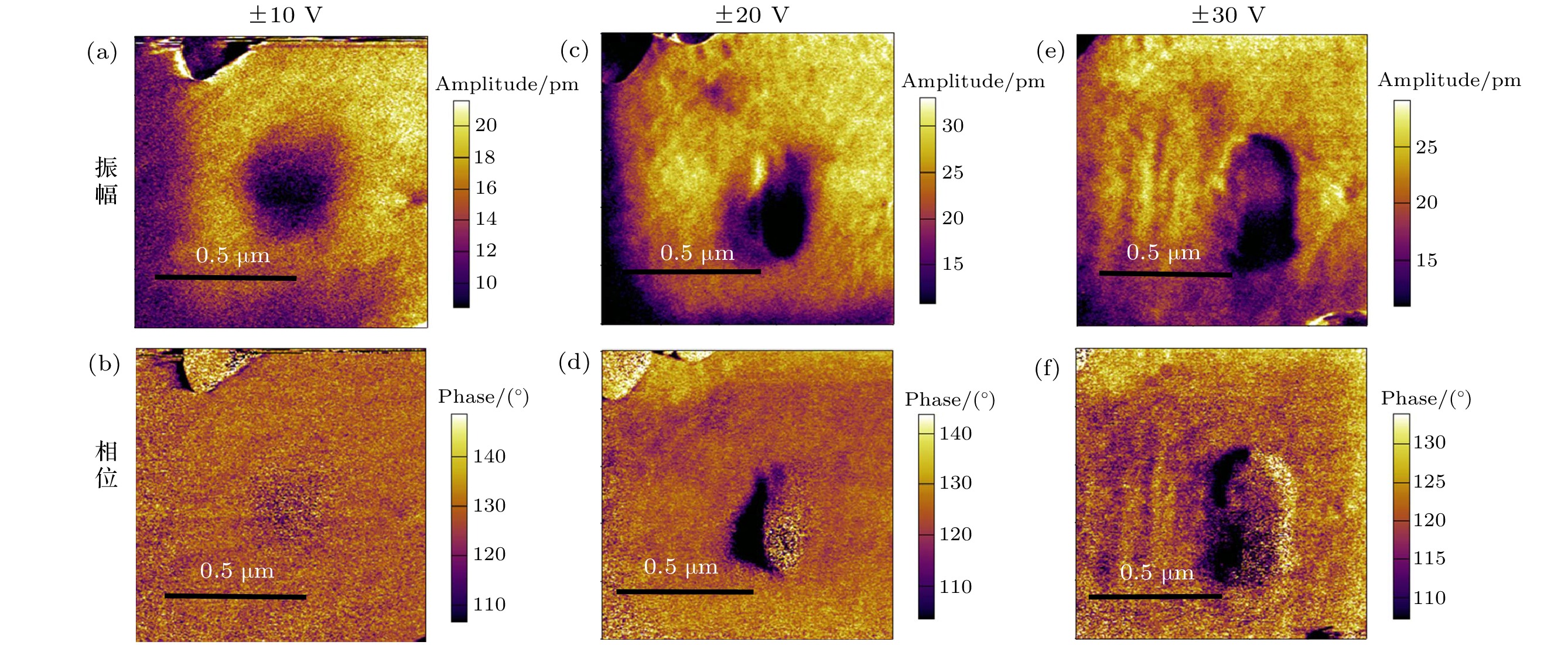 图 8 压电力显微镜下1 μm × 1 μm区域的结果 (a) ± 10 V电压下的面外振幅; (b) ± 10 V电压下的相位; (c) ± 20 V电压下的面外振幅; (d) ± 20 V电压下的相位; (e) ± 30 V电压下的面外振幅; (f) ± 30 V电压下的相位
Figure8. Results of 1 μm × 1 μm area under the piezoelectric force microscope: (a) Out of plane amplitude at ± 10 V; (b) phase at ± 10 V; (c) out of plane amplitude at ± 20 V; (d) phase at ± 20 V; (e) out of plane amplitude at ± 30 V; (f) phase at ± 30 V.
其中相位图中包含两种不同的颜色, 代表两种不同的极化方向. 可以发现Mn-PIMNT单晶复合材料在± 30 V的原位直流电压下, 相位图出现180°的极化翻转, 如图8(f)所示, 这与Xie等[19]研究的Mn-PIMNT单晶在不同电场下的铁电畴结构演变规律一致. 但是, Xie等[19]施加的原位直流电压为± 25 V时相位图已经展示出180°的极化翻转, 而本研究施加的原位直流电压为± 30 V时相位图展示出180°的极化翻转, 造成± 5 V的原位直流电压差异的原因如下: 1)本研究在刻蚀过程中由于SF6等反应气体与Mn-PIMNT单晶发生了化学反应, 需要更大电场才能使压电复合材料的铁电畴结构完全翻转; 2)由于阵列化使Mn-PIMNT单晶阵元尺寸微米化, 造成铁电畴结构不连续, 施加更大电场才能使压电复合材料的铁电畴结构完全翻转.
因此, 本研究继续用压电力显微镜对1 μm × 1 μm的区域中任意一个单点进行局部极化, 测其局部电滞回线[31]. 通常局部电滞回线测量选择“关闭”模式, 从而排除静电力的作用, 得到压电产生的贡献. 如图9所示, 对这个单点施加50 V的直流偏置电压, 复合材料的相位角翻转接近180°, 表明了压电复合材料在此直流电压下局部极化较为完全, 表现出良好的压电响应. 在“关闭”的模式下, 从蝶形曲线可以发现最大位移量为400 pm, 进一步验证了该复合材料具有优异的压电响应. 微米尺度下优异的压电响应使高密度阵列超声换能器具有大带宽、高灵敏度等特征, 从而使超声换能器[32-35]成像的分辨率更高.
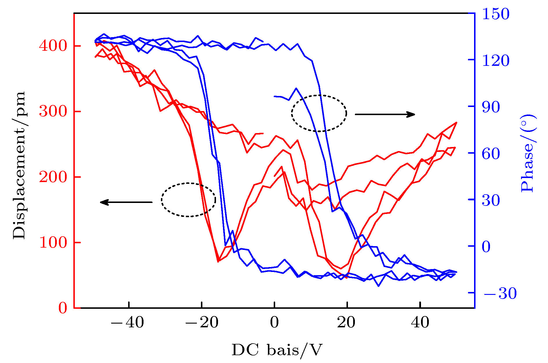 图 9 室温下1 μm × 1 μm区域内的原位电场诱导振幅和相位演化
Figure9. Electric field induced amplitude and phase evolution in situ in the 1 μm × 1 μm area at room temperature
