1.School of Materials Science and Engineering, University of Shanghai for Science and Technology, Shanghai 200093, China 2.National Laboratory of Infrared Physics, Shanghai Institute of Technical Physics, Chinese Academy of Sciences, Shanghai 200083, China
Abstract:In recent years, the research on topological materials, including topological insulator and topological semimetal, has received a lot of attention in condensed matter physics. HgCdTe, widely used in infrared detection, also holds huge potential in this field. It has been reported that the strained thin Hg0.865Cd0.135Te can realize topological insulator phase by using a CdZnTe substrate. However, the stress caused by changing substrate has great limitations. For example, the stress cannot be changed once the sample has been grown. Hence, we try to use a piezoceramics (PZT) instead to implement the stress and control the properties of HgCdTe. The main purpose of our experiment is to verify its validity. As is well known, the band structure of Hg1–xCdxTe can be precisely controlled by changing the content of Cd. When x lies between 0 and 0.165, HgCdTe features an inverted band structure, which is the premise of realizing topological phase. In this work, an inversion layer is induced on a single crystal grown HgCdTe bulk material by anodic oxidation, whose content of Cd is confirmed to be 0.149 by using XRD. Then the sample is thinned and attached to a PZT, which the tuning of stress is realized by applying a voltage to. Ohmic contacts are realized by indium in van der Pauw configuration. All measurements are carried out by using an Oxford Instruments 4He cryostat with magnetic field applied perpendicularly to the sample plane. At 1.5 K and zero voltage, an evident SdH oscillation is observed. By fitting the linear relationship between filling factor and the reciprocal of magnetic field, the concentration is obtained to be ${n_{\rm{s}}} = 1.25 \times {10^{16}}\;{{\rm{m}}^{ - 2}}$. Subsequently, we scan the voltage from 200 V to –200 V continuously in different magnetic fields. Two phenomena with different characteristics are observed. It is found that the resistance changes linearly with stress at zero field while an SdH oscillation-like behavior occurs at high field. We attribute such a difference to the existence of two conductive channels: one is the bulk material and the other is the two-dimensional electron gas. It is also noteworthy that the topological phase in our sample cannot be determined because the quantum Hall conductance is polluted by the conductance of bulk material. In conclusion, our results show that it is an effective way to use the PZT to tune the stress and this method can also be applied to the research of other materials. Keywords:HgCdTe/ Shubnikov-de Haas oscillation/ piezoceramics/ stress control
全文HTML
--> --> --> 1.引 言碲镉汞(Hg1–xCdxTe)是一种窄禁带直接带隙半导体材料, 是由均具有闪锌矿立方晶体结构的正禁带CdTe和负禁带HgTe按照比例形成的赝二元化合物材料, 具有禁带宽度随组分可调、光吸收率高、电子迁移率高和热产生率较低的优点. 通过调控禁带宽度, 可使其红外探测范围覆盖从近红外到甚长波红外波段(0.7—30.0 μm)[1,2]. 由于上述的诸多优点, 这一材料目前被广泛应用于各红外探测领域. 此外, 碲镉汞电子有效质量小, 有效g因子大, 具有很强的自旋轨道耦合作用[3,4], 使它成为制备自旋器件的理想材料. 在基础研究方面, HgCdTe材料也具有重要的意义. 2006年, 张守晟[5,6]团队预言了量子自旋霍尔绝缘体可于HgCdTe量子阱结构中实现, 并随后在实验上验证了这一预言. 近年来还有研究显示, 通过调控应力有望在HgCdTe中实现拓扑绝缘体与拓扑半金属态[7-9]. 半导体的电学性质可以通过多种手段调控, 包括栅压、光照以及应力调控. 其中, 栅压与光照都可直接调控载流子, 而应力调控则是间接调控. 此外, 相比于前两者, 要在低温下实现对样品的应力调控是极具挑战性的. 传统的方法是在不同的衬底上生长同一材料, 但这一方法具有很大的局限性, 不仅耗时耗力, 而且应力的调控完全取决于样品与衬底的晶格常数的关系, 无法人为直接调控. Shayegan等[10]提出了利用压电陶瓷对低温下的样品进行原位应力调控的方案, 并成功在AlAs量子阱输运测试中实现了有效的调控. 此后, 这一调控方案被用于多种材料的输运测试实验中, 已报道过的有: GaAs量子阱[11-13]、InGaAs量子点[14]、 二维材料MoS2[15]和InAs/GaSb双量子阱结构[16]等. 目前关于HgCdTe的输运性质调控主要是栅压与光照. 魏来明等[17]在受到微波辐照的HgCdTe薄膜中观测到了增强的退相干时间. Palm等[18]在HgCdTe基的场效应晶体管中观察到了反弱局域效应, 并成功用栅压调控自旋轨道耦合强度. 高矿红等[19]实现了用栅压对Hg0.78Cd0.22Te薄膜反型层中的自旋分裂能在6.95—9.06 meV之间的调控. 据我们所知, 使用压电陶瓷对这一材料体系进行应力调控的研究还未有报道. 本文通过对粘贴在压电陶瓷上的HgCdTe样品进行低温磁输运测试, 观测到了明显的SdH振荡, 表明反型层处形成了较高质量的二维电子气. 通过压电陶瓷的应力调控, 分析了零磁场与高磁场下的调控数据并对相应的应力调控机制进行了讨论. 2.实 验通过单晶生长制备了HgCdTe体材料, 将样品在碱溶液中进行阳极氧化, 使其在表面形成氧化层, 该氧化层可以将样品表面与空气隔离以保护样品; 另外可以使材料表面发生钝化, 从而在氧化层与HgCdTe材料的交界处形成反型的二维电子气. 通过X双晶射线衍射确定样品组分x. 然后使用环氧树脂胶将样品粘贴在压电陶瓷的工作面上, 50 ℃气氛下加热固化, 且反型层靠近压电陶瓷的工作面. 由于样品本身厚度较大, 因此通过手工研磨的方法将样品减薄, 以确保压电陶瓷的拉伸或收缩能对样品的应力进行调控. 最后得到的样品结构如图1所示, 当对压电陶瓷施加正偏压时, 样品应受拉伸应力. 图 1 样品结构示意图, 其中箭头表示对压电陶瓷施加正偏压时的应力方向 Figure1. Schematic diagram of the sample, and the arrows indicate the direction of strain when positive voltage is applied.
实验测量采用范德堡测试法[20], 样品规格约为4 mm × 3 mm, 以金属铟在方形样品的四个顶角上制作四个电极以形成欧姆接触, 并使用银线引出接线. 所使用的低温超导磁体系统为Oxford公司的Teslatron设备, 施加的磁场垂直于薄膜面, 温度维持在1.5 K, 磁场最高可达8.9 T. 测量时使用了有效值为1 μA, 频率为16.666 Hz的低频恒交流源, 再通过锁相放大器SR830来测量磁阻以获得样品的电阻数据. 调控压电陶瓷所使用的电压源为Keithley 2400, 其可施加的最大电压范围为–200—200 V.
由此可以得到样品的组分x = 0.149. 图 2 样品的X射线双晶衍射曲线 Figure2. DCXRD of the sample.
图3(a)给出了样品在1.5 K温度下未受压电陶瓷应力调控时的纵向电阻ρxx随磁场的变化曲线. 如图3(a)所示, 纵向电阻在高场部分显示出了良好的SdH振荡特性, 表明在氧化层与HgCdTe界面处确实形成了较高质量的二维电子气. 为了排除体材料部分对振荡的影响, 对纵向电阻进行去背底处理, 如图3(b)所示. 图 3 (a) 1.5 K温度下, HgCdTe样品在磁场中的SdH振荡图; (b)去背底处理后的SdH振荡曲线 Figure3. (a) The longitudinal resistance of HgCdTe as function of magnetic field at 1.5 K; (b) remove the background resistance from SdH oscillations.
根据理论, 填充因子满足$\nu = 2{E_{\rm{F}}}/\left( {{{\rm{\hbar}}\omega _{\rm{c}}}} \right)$, 其中${E_{\rm{F}}} = {\hbar^2}k_{\rm{F}}^2/\left( {2{m^*}} \right)$($\hbar$代表普朗克常量, EF代表费米能级, 为电子的回旋共振频率, kF为费米波矢, m*为电子有效质量), 因此, 可以得到填充因子ν与磁场倒数1/B满足正比关系: $\nu = \left( {hn/e} \right)\cdot\left( {1/B} \right)$. 通过对填充因子与磁场倒数的线性拟合, 如图4所示, 所有的点都在直线附近, 表明拟合结果较好. 由此可以计算出反型层二维电子气的电子浓度${n_{\rm{s}}} = ke/h = 1.25 \times {10^{16}}\;{{\rm{m}}^{ - 2}}$. 同时, 也可反推图3中各个峰与谷的填充因子, 部分填充因子已标注在图3及图4中. 图 4 填充因子ν与磁场倒数1/B的变化关系及拟合直线 Figure4. Relationship between the filling factor ν and the reciprocal 1/B of the magnetic field and the fitting line.
图5分别给出了1.5 K温度下样品在零磁场下电阻随压电陶瓷偏压的变化关系以及8.9 T磁场下去背底后的电阻随压电陶瓷偏压的变化. 由图5可以明显地看到, 样品的电阻随压电陶瓷上的栅压变化而发生变化, 表明样品受到了应力作用, 从而验证了压电陶瓷调控应力这一手段的有效性. 此外, 在0 T时样品的电阻变化量十分小, 且为单调变化; 而在高场时, 变化量增大且表现出了振荡的特征. 这一区别的来源可能是由于样品内部存在着体材料与二维电子气的平行电导[22,23], 在低磁场时, 电阻由体材料电阻主导, 而体材料由于离压电陶瓷工作面较远, 因此受到的应力影响较小; 而当样品处于高磁场条件下, 体材料电阻由于正磁阻效应变得很大, 而二维电子气发生的是SdH振荡, 其电阻相对较小, 从而在样品的电阻中占主导地位, 因此强磁场下的电阻变化曲线主要反映了二维电子气随应力变化的性质. 对于体材料而言, 应力调控会使其能带结构发生变化. 从图5(a)可以看到当施加正偏压, 即对样品产生拉伸应力时, 电阻变小; 相反, 收缩应力使得电阻变大. 这里应力应是改变了能带的带隙[8,24], 当施加拉伸应力时, 带隙减小而费米能级不变, 因此导带中的电子浓度增加, 从而使得体材料的电阻减小; 反之当应力为压缩应力时, 电子浓度则会因为带隙的增大而减小. 图 5 1.5 K温度下样品在不同磁场条件下电阻随压电陶瓷偏压的变化 Figure5. Voltage dependence of resistance under different magnetic field at 1.5 K.


 图 1 样品结构示意图, 其中箭头表示对压电陶瓷施加正偏压时的应力方向
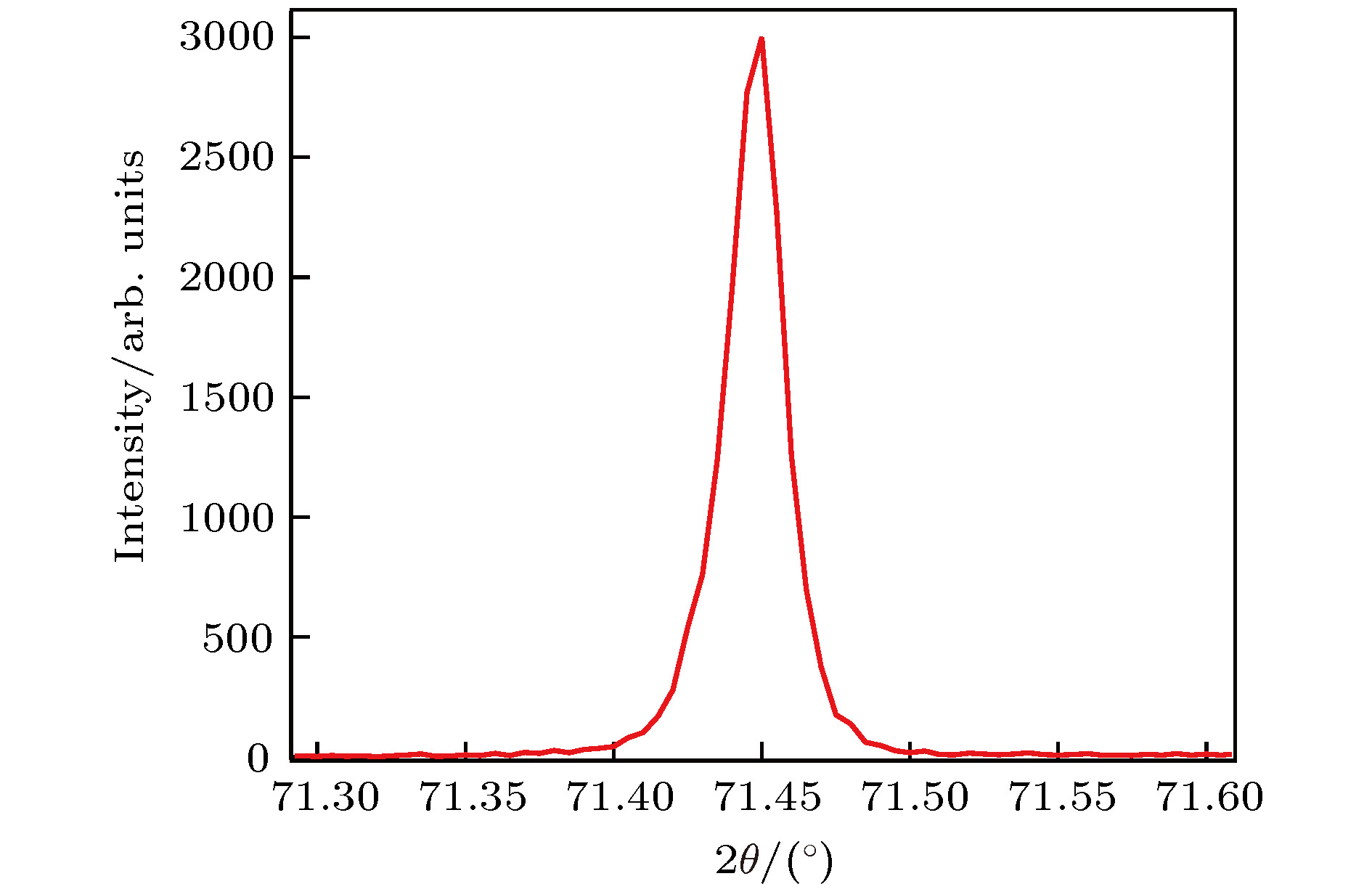 图 2 样品的X射线双晶衍射曲线
 图 3 (a) 1.5 K温度下, HgCdTe样品在磁场中的SdH振荡图; (b)去背底处理后的SdH振荡曲线


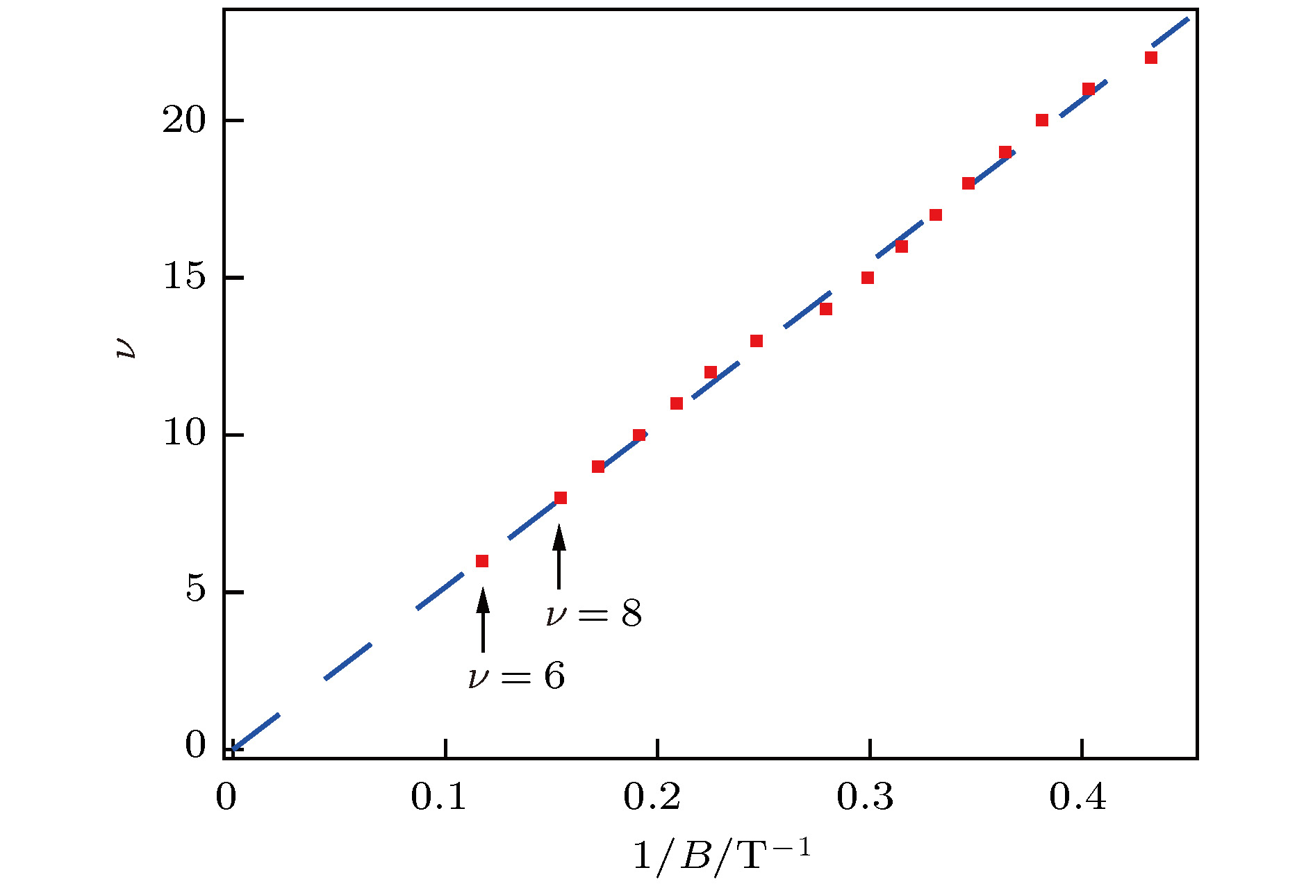 图 4 填充因子ν与磁场倒数1/B的变化关系及拟合直线
 图 5 1.5 K温度下样品在不同磁场条件下电阻随压电陶瓷偏压的变化
