Fund Project:Project supported by the Key Program of the National Natural Science Foundation of Zhejiang province, China (Grant No. Z19F040002), and the Key Research and Development Program of Zhejiang province, China (Grant No. 2019C01158)
Received Date:28 July 2019
Accepted Date:14 August 2019
Available Online:19 August 2019
Published Online:20 August 2019
Abstract:As the feature size of Metal-Oxide-Semiconductor Field Effect Transistors (MOSFETs) continues to decrease, large numbers of new problems appear. Techniques such as strain project, new channel materials and new device structures are considered by academics and industry to be effective ways to continue to improve device performance. In this paper, the scattering mechanism of carriers in the device channel is studied from three aspects: strain technique, new channel material and new structure device: (1) strain technique: Biaxial tensile strain can change carrier distribution among different energy levels, which affects Coulomb scattering and Coulomb mobility. Furthermore, from the TEM image, it is found that biaxial tensile reduces the channel surface roughness for Si nMOSFET, leading an enhancement of electron mobility. However, no such similar phenomena were observed in pMOSFET. Based on this, a new method for calculating the mobility of MOSFET surface roughness scattering using TEM image has been proposed. (2) New channel material: In the germanium (Ge) transistors with different crystal faces, the scattering mechanisms of electron under high field conditions are different. The phonon scattering dominates the Ge(100) transistor, while the surface roughness scattering dominates the Ge(110), (111) transistors. This result is quite different from Si MOSFET. Therefore, a unified model for the scattering mechanism of electron in Ge nMOSFET has been proposed. In SiGe transistors, alloy scattering mainly play a role in the region with relatively small effective electric field (Eeff). The strength of alloy scattering would be weakened in high field and could be decreased by reducing the thickness of SiGe layer. (3) New structure devices: In ultra-thin body germanium (GeOI) transistors, carrier transport is influenced by high- k /channel interfaces, as well as Ge channel/buried oxide (BOX) interface. As the Ge layer thickness decreases, carrier distribution is closer to the interfaces, which intensifies Coulomb scattering and surface roughness scattering. As a result, the mobility in GeOI transistor decreases as the thickness scaling. In addition, the distribution of electron in different energy valleys changes with the thickness decrease in Ge layer, which affects the scattering of electrons. When the Ge film is lower than 10 nm, a part of electron in the L valley will move to the Γ valley, causing the decrease of electron effective mass and increasing the electron mobility. Keywords:carrier scattering/ strain technique/ new channel materials/ newstructure transistors
全文HTML
--> --> --> 1.引 言近几十年来, 硅(Si)基集成电路技术一直遵循着摩尔定律在高速发展(图1). 目前量产级的硅金属-氧化物-半导体场效应晶体管(metal-oxide-semiconductor field effect transistor, MOSFET)等效沟道长度已经接近10 nm, 进一步减小沟道长度将导致晶体管出现短沟道效应、速度饱和效应、介电击穿等一系列负面现象, 通过缩小器件尺寸来延续半导体技术进步的传统发展模式正面临硅材料物理极限的挑战. 因此, 学术界和产业界提出了一些新的晶体管技术来继续推动摩尔定律的发展, 包括应变技术、新沟道材料和新结构器件 [1—5]等. 图 1 集成电路技术节点随时间的演进, 图中提取了90 nm到10 nm技术节点 Figure1. Evolution of integrated circuit technology nodes: from 90 nm to 10 nm.
我们研究了双轴拉伸应变对Si pMOSFET中衬底掺杂浓度和界面态限制的库仑散射迁移率(μsub和μit)[17]. 研究发现, 对于双轴拉伸应变Si pMOSFET来说, 随着衬底浓度的增大, 重空穴能级和轻空穴能级互相靠近, 加剧了谷间散射, 导致沟道空穴迁移率降低(图2(a)). 此外, 还有一个重要的库仑散射来自于界面态(Dit), 研究结果表明, 双轴拉伸应变提高了载流子在轻空穴能级的占据概率. 由于轻空穴能级上的载流子垂直于界面的有效质量比重空穴能级要小, 其在沟道中的分布也更远离界面, 因此拉伸应变能够降低由界面态引起的库仑散射(图2(b)). 而对于双轴拉伸应变的Si nMOSFET来说, O. Weber 等人证明情况刚好相反,应变降低了 μit且提升了 μsub[18]。 图 2 (a) 拉伸应变和衬底浓度对空穴子能带结构的影响; (b) 双轴拉伸应变对电子空穴μit影响的示意图[17] Figure2. (a) Effects of tensile biaxial strain and Nsub on the hole subband structure; (b) schematic diagram of the interpretation for the effect of biaxial tensile strain on μit of electrons and holes[17].
22.2.应变技术对表面粗糙度散射的影响 -->
2.2.应变技术对表面粗糙度散射的影响
对于工作在高场下的Si MOSFET来说, 沟道表面粗糙度散射是影响器件迁移率的主要因素[19]. 衬底掺杂浓度的提高会引起晶体管工作电场的增大,使得表面粗糙度散射对晶体管载流子输运的影响也越来越显著。我们系统地研究了双轴拉伸应变对表面粗糙度的影响,以及由此导致的电子和空穴迁移率的变化[20]. 根据电子和空穴表面粗糙度散射限制迁移率在不同应变下的实验结果, 发现双轴拉伸应变能降低电子的表面粗糙度散射, 但是并没有降低空穴的表面粗糙度散射, 如图3所示. 进一步地, 我们利用超高分辨率的透射电镜(TEM)技术表征了无应变硅和应变硅晶体管的沟道/氧化物界面, 结果发现, 由于硅衬底中存在应力, 应变硅晶体管的表面粗糙度显著比无应变硅的小(图3(b)), 从而减弱了电子的表面粗糙度散射. 在此基础上, 提出了一种新的利用TEM图像计算MOSFET表面粗糙度散射影响迁移率的方法[21], 利用该方法计算得到的表面粗糙度限制迁移率与实际在低温下的测试结果基本吻合. 图 3 (a) 应变对电子和空穴表面粗糙度散射的影响; (b) 无应变硅和应变硅沟道表面粗糙度[20] Figure3. (a) Low-temperature electron and hole mobility versus Ns for Si and s-Si with different amounts of strain; (b) TEM photographs of Si and s-Si (10% Ge and 35% Ge) Si/SiO2 interfaces[20].
3.新沟道材料23.1.Ge nMOSFET中电子的散射机制 -->
3.1.Ge nMOSFET中电子的散射机制
不同于Si, Ge nMOSFET由于高场下载流子在Δ能谷中的占据率提高, 会引入L能谷与Δ能谷的谷间散射, 导致了高场散射机制的复杂化. 我们研究了Ge(100), (110), (111) nMOSFET中电子的库仑散射和表面粗糙度散射[22]. 通过自洽求解薛定谔-泊松方程, 并结合实验测试结果, 计算分析了电子的声子散射限制迁移率(μph)和表面粗糙度散射限制迁移率(μsr), 提出了Ge沟道中电子的散射机制的统一模型(图4). 对于Ge(100) nMOSFET, 高场下声子散射仍然是影响晶体管迁移率的主要散射机制, 而非表面粗糙度散射. 因此, 仅仅改善界面的粗糙度很难有效地提升Ge(100) nMOSFET的高场迁移率. 而对于Ge(111)和(110) nMOSFET, 在高场下, 谷间散射减小, 同时载流子重新分布进入具有较高μph的L//能谷, 因而可以通过改善表面粗糙度来提升电子的高场迁移率. 图 4 不同晶面的Si及Ge nMOSFET中的电子输运模型[20] Figure4. Electron transport models in Si and Ge nMOSFETs with different crystal faces[20].
23.2.SiGe量子阱pMOSFET中的合金散射 -->
3.2.SiGe量子阱pMOSFET中的合金散射
由于SiGe衬底具有很高的空穴迁移率, 并且与Si基金属氧化物半导体(CMOS)工艺兼容性较高, 因而采用SiGe沟道的pMOSFET是目前新材料器件研究领域的热点之一[23]. 我们研究了sSi/Si0.5Ge0.5/sSOI量子阱pMOSFET输运特性, 分析了SiGe量子阱pMOSFET中空穴的分布, 提取了在室温和低温下的空穴迁移率(图5(a)), 并利用以下公式来研究合金散射对空穴迁移率的影响: 图 5 (a) SiGe量子阱pMOSFET在300 K和15 K下的迁移率; (b) 根据实验结果计算出的SiGe量子阱pMOSFET中空穴μalloy+phonon随Ninv的变化[23] Figure5. (a) Extracted effective hole mobilities of the QW p-MOSFET at 15 and 300 K; (b) μphonon+alloy obtained from the extracted hole mobility at 300 and 15 K[23].
W. H. Chang 等人研究了 GeOI nMOSFET 电子迁移率随沟道厚度的变化情况[26]。研究发现,当沟道厚度大于 10 nm 时,随着厚度的变薄,电子受到的库伦散射和表面粗糙度散射愈加明显,因此电子迁移率随 Ge 膜厚度减小而降低(图8(a)); 而当Ge膜低于10 nm时, 由于量子效应, 电子在能级中的占据率会重新分配, L能谷中的一部分电子会跃迁至Γ能谷, 引起了电子有效质量的减小, 从而提升迁移率(图8(b)). 图 8 (a) 电子迁移率与Ge厚度关系; (b) 不同Ge厚度下电子在能级中的分布情况[26] Figure8. (a) Tbody dependence of effective electron mobility characteristics; (b) band structure of UTB GeOI nMOSFET under different channel thickness[26].
5.结 论本文从应变技术、新沟道材料和新器件结构三个角度研究了载流子输运中的散射机制。应变技术可以有效提高载流子迁移率,但是对于电子和空穴的作用不同。在低场时,双轴拉伸应力减弱了衬底掺杂对电子的库仑散射,但增强了对空穴的库仑散射,同时,双轴拉伸应力提高了界面态对电子的散射,降低了界面态对空穴的散射;在高场时,双轴张应力降低了电子的表面粗糙度散射,但是并没有降低空穴的表面粗糙度散射,该结果通过一种新的利用 TEM 图像计算 MOS器件粗糙度散射影响的迁移率的方法得到验证。对于Ge nMOSFET,电子在不同晶面的 Ge 沟道中受到的散射机制不同,Ge (100) nMOSFET 在高场条件下声子散射仍然是影响迁移率的主要散射机制,而在 Ge (111)、 (110) nMOSFET 中,表面粗糙度散射占主导地位。在 SiGe 量子阱 pMOSFET 中,合金散射主要作用于有效电场强度比较小的区域,而对高场迁移率影响不大。对于GeOI MOSFET,由于存在上下两个界面,载流子输运会受到上下两个 MOS 界面的散射,其作用机理更加复杂,界面质量及 Ge 膜厚度均影响载流子的散射过程。
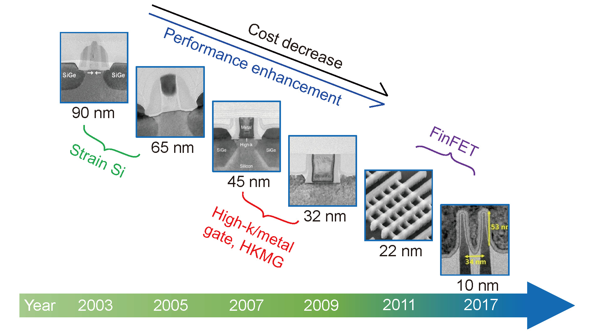 图 1 集成电路技术节点随时间的演进, 图中提取了90 nm到10 nm技术节点
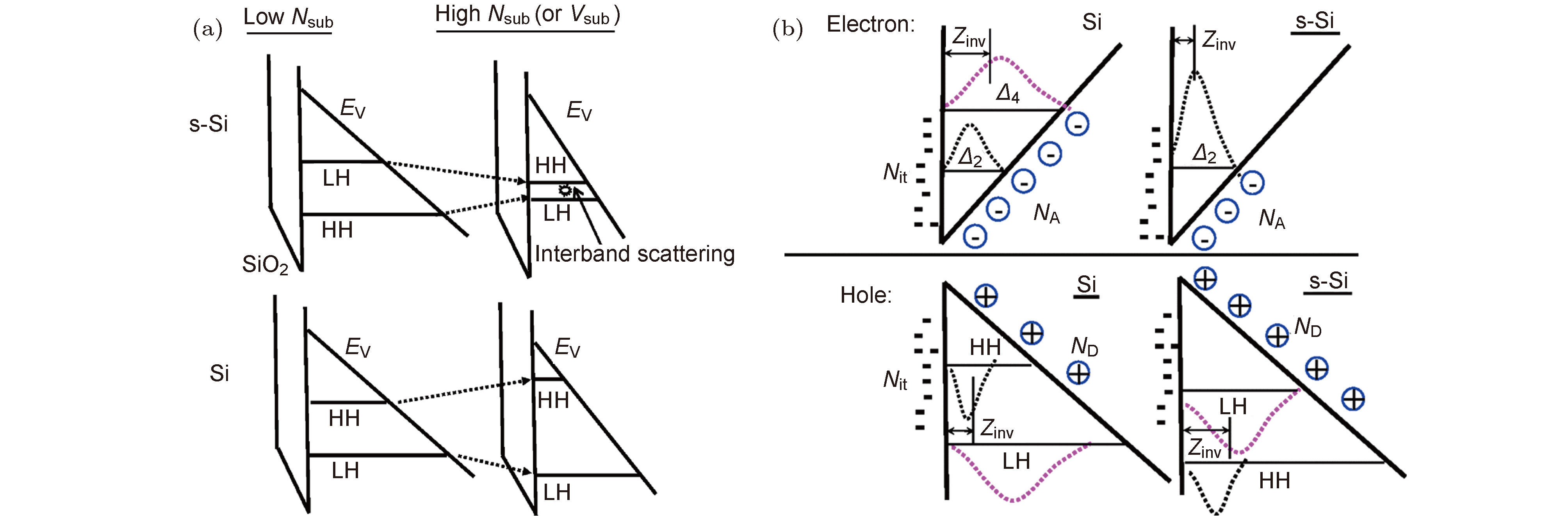 图 2 (a) 拉伸应变和衬底浓度对空穴子能带结构的影响; (b) 双轴拉伸应变对电子空穴μit影响的示意图[17]
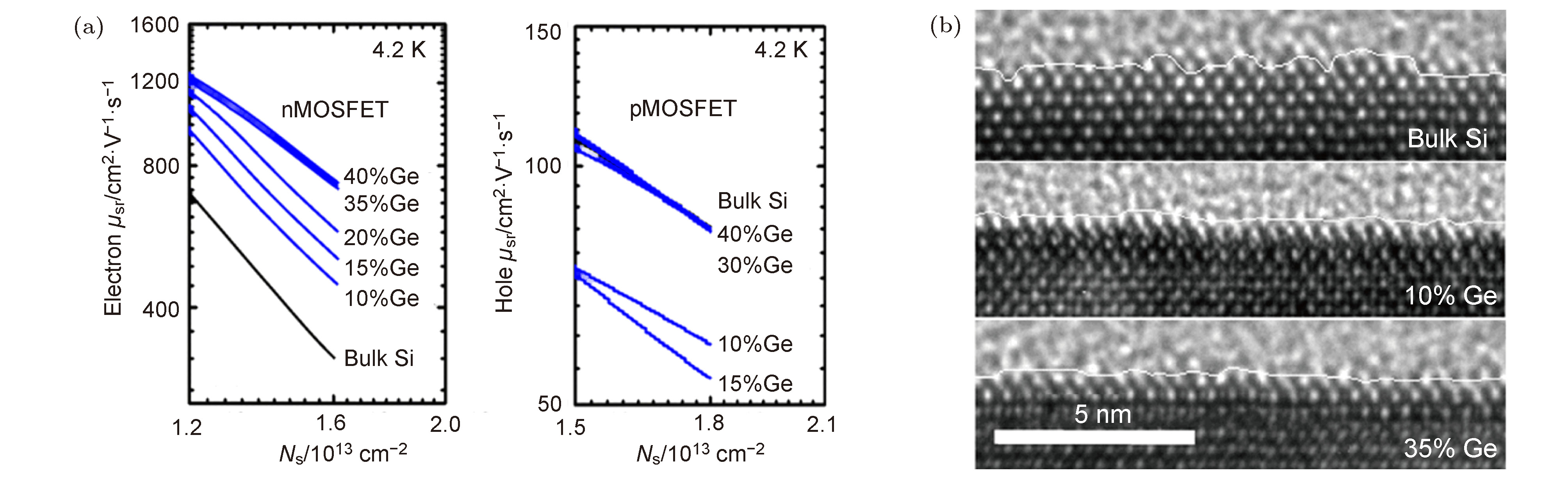 图 3 (a) 应变对电子和空穴表面粗糙度散射的影响; (b) 无应变硅和应变硅沟道表面粗糙度[20]
 图 4 不同晶面的Si及Ge nMOSFET中的电子输运模型[20]
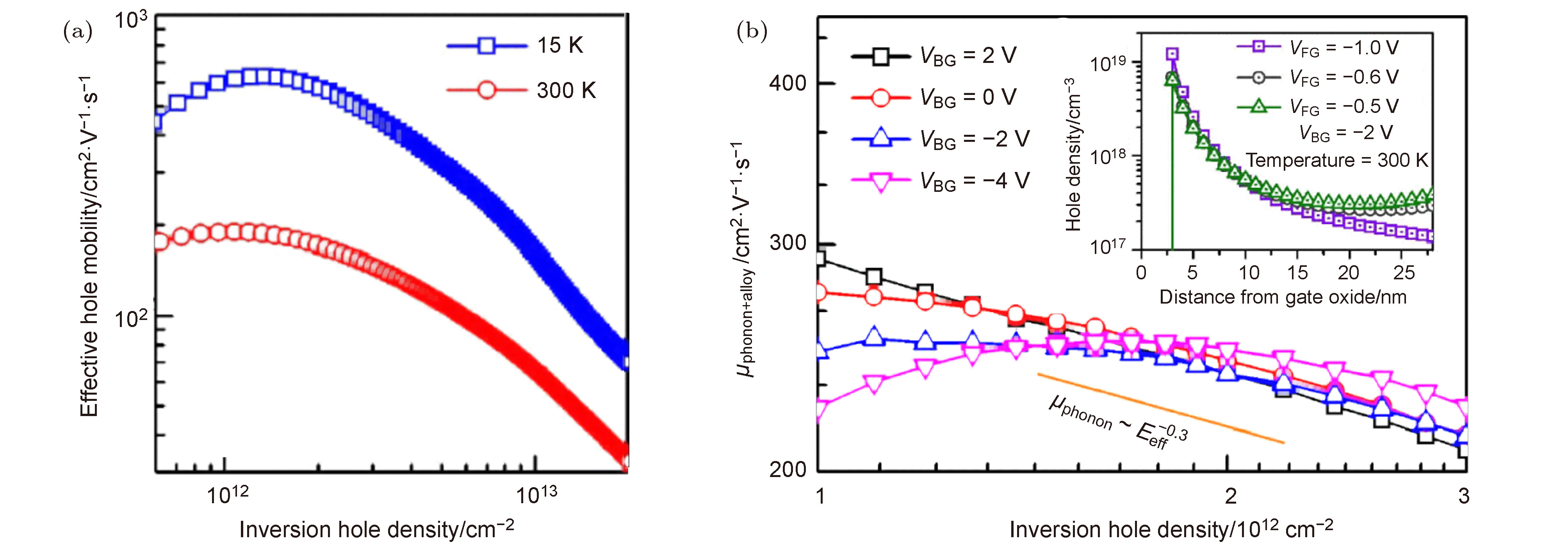 图 5 (a) SiGe量子阱pMOSFET在300 K和15 K下的迁移率; (b) 根据实验结果计算出的SiGe量子阱pMOSFET中空穴μalloy+phonon随Ninv的变化[23]
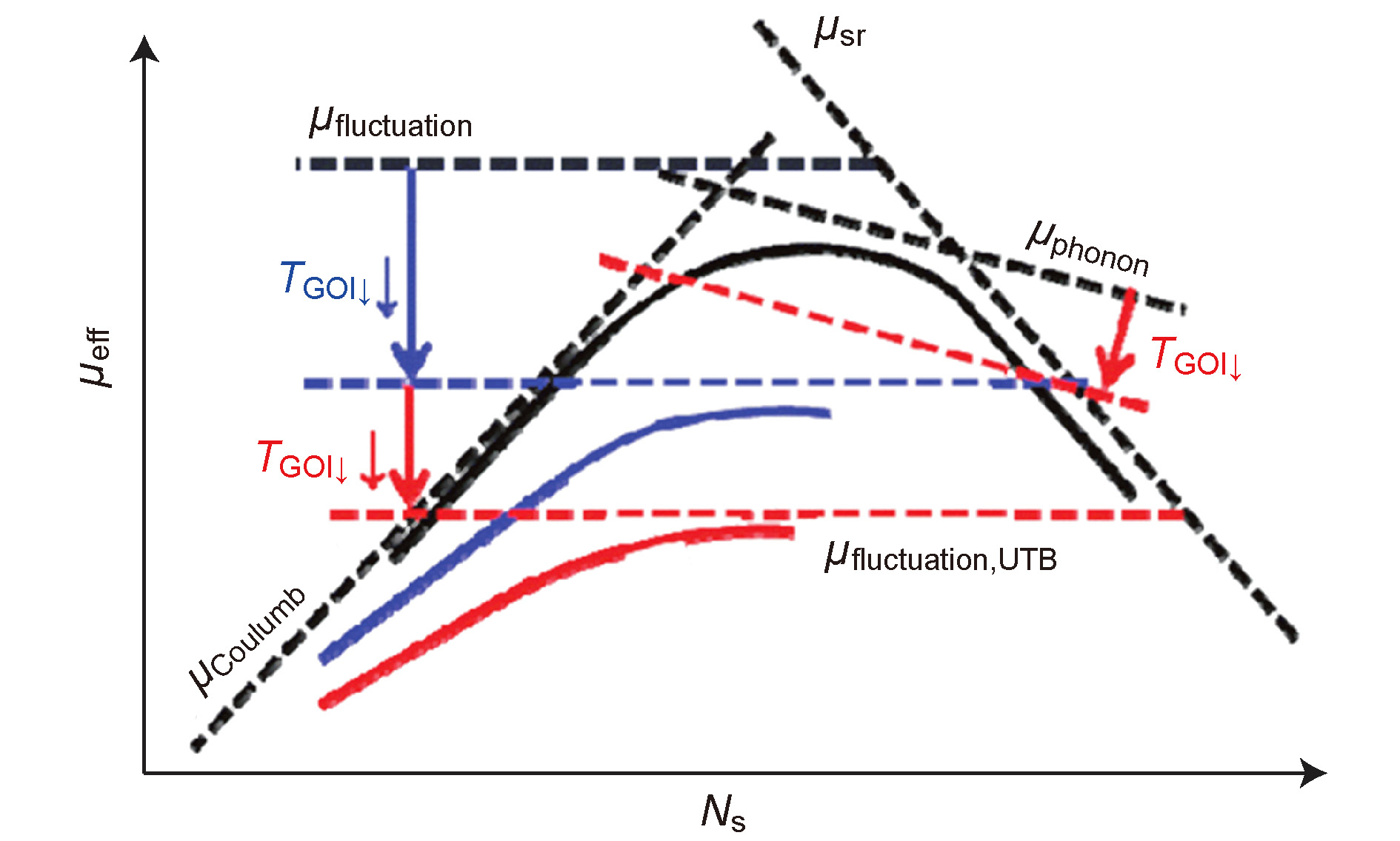 图 6 超薄GeOI 晶体管中的载流子输运模型[24]
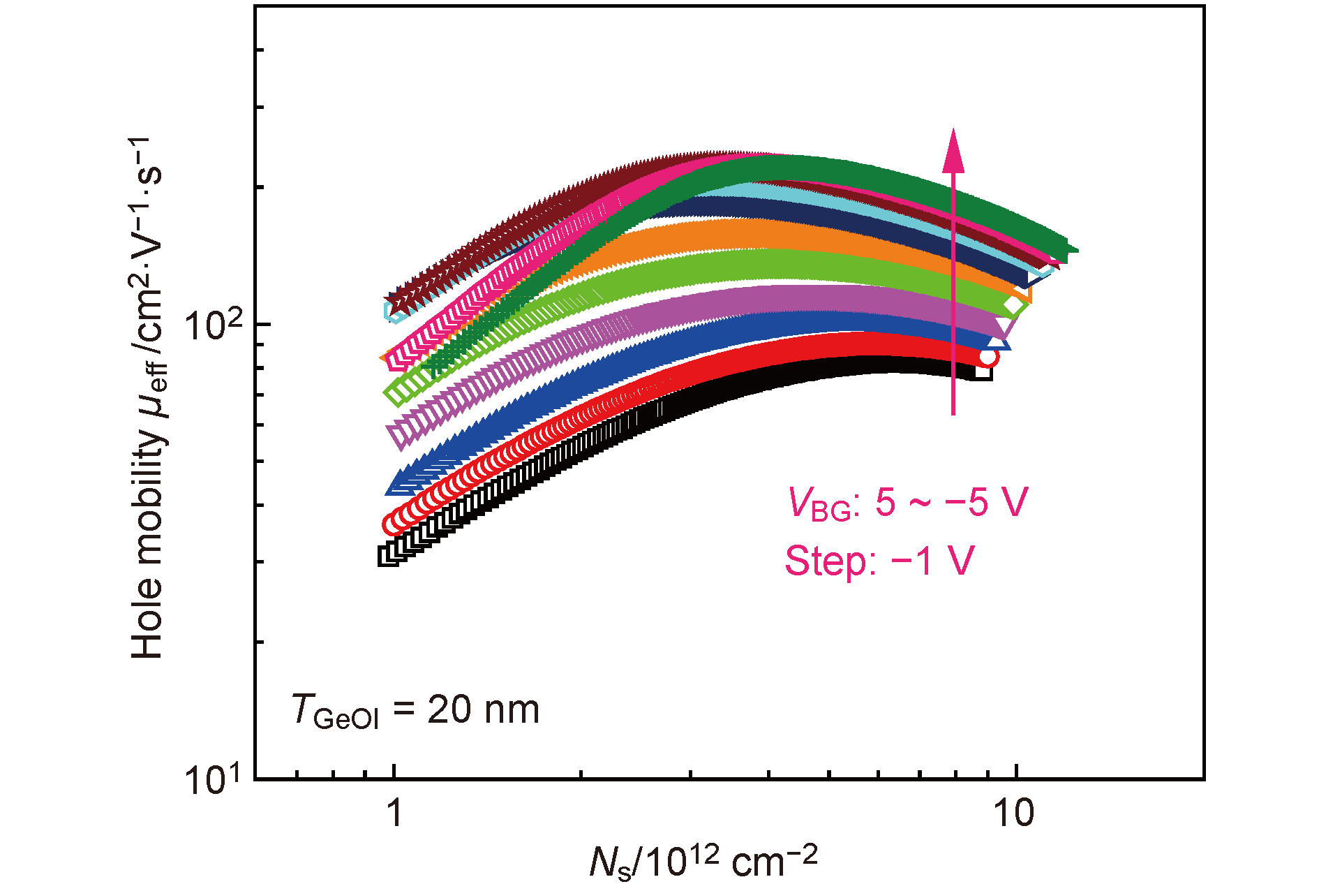 图 7 GeOI pMOSFET空穴有效迁移率随VBG的变化情况[23]
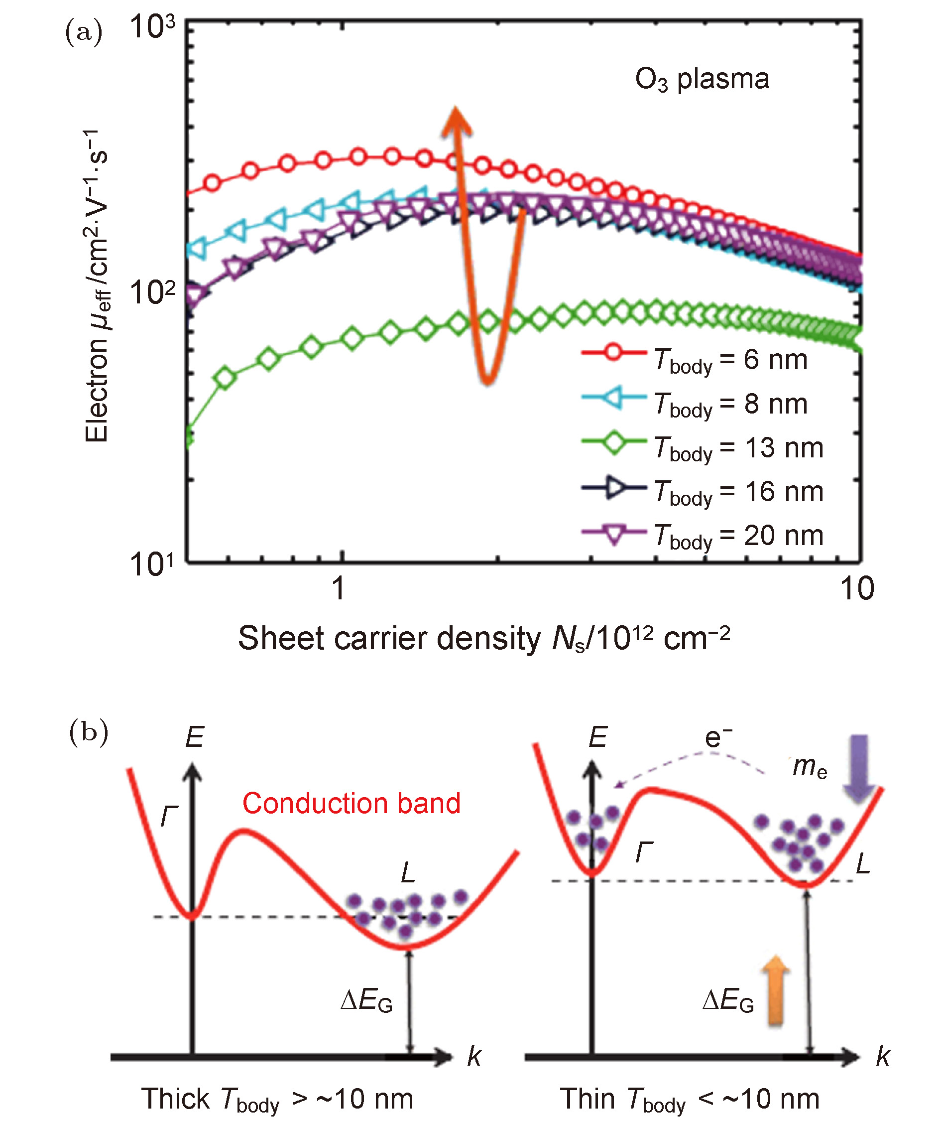 图 8 (a) 电子迁移率与Ge厚度关系; (b) 不同Ge厚度下电子在能级中的分布情况[26]